© 2019, IRJET | Impact Factor value: 7.211 | ISO 9001:2008 Certified Journal
| Page 1322
SIMULATION OF 10 NM DOUBLE GATE MOSFET USING VISUAL
TCAD TOOL
Aashaq Hussain Kuchy
1, Mehraj Ud Din Wani
21
M.Tech Student, Department of Electronics Engineering, Lovely Professional University, Punjab, India
2M.Tech Student, Department of Electrical Engineering, Lovely professional University, Punjab, India
---***---Abstract -Evolution of Silicon technology has revolutionized the semiconductor industry. The characteristics of MOSFET has been subsequently degraded by continuous scaling. A Double gate MOSFET is proposed to overcome the limitations of conventional MOSFETs. Due to continuous scaling MOSFET’s performance are highly effected by short channel effects. These short channel effects (SCE) are responsible for reduction of gate coupling to the channel. In order to improve gate coupling, a double gate MOSFET is being proposed in this work and its comparative analysis is done using Cogenda TCAD genius simulator. In this work our main focus is to perform simulation of 10 nm Double gate MOSFET on Visual TCAD software and to extract the transconductance, DIBL, Ion –Ioff ratio and other important parameters of the device.
Key words: Short channel effects (SCE), Drain induced barrier limiting (DIBL), Visual TCAD, Double gate MOSFET.
1. INTRODUCTION
[image:1.595.115.479.430.703.2]Since three decades or more MOSFETS have been continually scaled down from micrometer to nanometer range and from nanometer to sub nanometer range to validate Moore’s law as shown in Figure 1. According to Moore the count of transistors are doubled in every eighteen months which of course enhances the processing power of device almost twice in every eighteen months [1].Today due to scaling we are able to put together billions of transistors on single chip. However reducing the gate length below certain limits results in loosing of control of gate over channel because of presence of SCEs [2].
Figure 1:Moore’s law[2]
Various conventional techniques has been observed by researchers for the reduction of these SCE these include, reducing gate oxide thickness and using high k dielectric gate oxide like HfO2. But all these have limitations reducing oxide thickness
increases leakage current which leads to increase in static power dissipation. Below 20 nm with reduced oxide thickness tunneling current is more common which increases power dissipation. Using HfO2 increases compatibility issues with
© 2019, IRJET | Impact Factor value: 7.211 | ISO 9001:2008 Certified Journal
| Page 1323
multi gate MOSFET, Finfet, Gate all-around MOSFETs etc. These multi gate MOSFETS has been used to overcome the limitations of single gate MOSFETs. Double gate Mosfets reduces leakage current subthreshold slope and DIBL parameters, therefore having clear dominance over single gate MOSFET. The Double gate MOSFET having two gate terminals along with two gate oxides which lies above and below the substrate as shown in Figure 2.Fig 2: Double gate MOSFET structure.
Due to presence of two gates the electrostatic control of gate over channel is increased. Which results in increase of drain and is almost twice when compared to single gate Mosfet.Because of presence of two gates, between source and drain electric field lines are omitted. The main focus of Double gate MOSFET is to gain maximum control over the silicon channel very effectively by proper selection of channel width and by applying proper gate voltage. It has been observed that increasing the number of gates provides better control over channel and their by improving device performance [3-6].
1.1 Double Gate Mosfet Operation
Double gate MOSFET having mostly undoped conducting channel with gate terminals surrounding this conducting channel in order to make sure that each part of channel is very close to the gate terminal [7]. When the voltage is applied at the gate terminals two conducting channels are created which are very close to the Si-SiO2 Interface. The electric field is
controlled by applied gate voltage their by defining the amount of current passing through the channel. Based upon the application of gate voltage we have two types of Double gate MOSFETs
[image:2.595.117.465.163.392.2]Symmetrical DG MOSFETs: A DG is said to be symmetrical when at both gates same input voltage is applied and when both are of same work function as shown in Figure 3. In on state, at same gate voltage two Conducting channels are created above and below the Si substrate, Conduction occurs simultaneously in both these channels [8].
© 2019, IRJET | Impact Factor value: 7.211 | ISO 9001:2008 Certified Journal
| Page 1324
Asymmetrical DG MOSFET: A DG is said to be asymmetrical when different voltages are applied at gate with same work function or same voltages are applied at gate with different work functions as shown in Figure 4.In this only single channel is created and at a very high operational voltage another inversion channel may be created. Switching is obtained when different gate voltages are applied at gate terminals [9].Figure 4: Asymmetrical DG MOSFET [3]
1.2 Short channel Effects:
With devices scaled below sub nanometer range, the source an drain terminals are so close that their presence decreases the control of gate over channel and hence reduces current flow in the channel. Therefore the undesirable effects called short channel effects are introduced in the device.
DIBL: For short channel devices DIBL effect occurs when depletion region of S/D starts interacting which results in lowering of potential barrier .A little increase in drain voltage further reduces this barrier. Therefore an additional carriers are injected into the channel region but this increase in carrier concentration is function of drain voltage and not of gate voltage [10].
DIBL= ………..i
Subthreshold Slope: When Vgs is lower than Vth it is believed that transistor should be completely in off state, but actually a small and weak inversion channel exits due to which a small current flows between source and drain and transistor is said to be operating in subthreshold region. The minority concentration is very less in weak inversion region. The scalability limit of device is determined by this subthreshold slope parameter [11-14].
SS= (d(log Ids)/dVgs)-1………..ii
1.3 COGENDA TCAD TOOL:
Cogenda TCAD tool is a GUI for device simulation. Cogenda tool is designed in order to suit with every user and every student, and its main focus on the ease of use. TCAD tool is very easy to use, command line or coding are also used. Beginners need a very less time just a few minutes to get started. At the same time doesn’t sacrifices the power of Genius simulator. Various physical models and various options can be accessed with this TCAD tool. This TCAD tool is capable of doing 2D as well as 3D device simulations.
For our simulation purposes we have used Cogenda TCAD tool, which is basically a device simulator tool. In this tool we can design any structure and can visualize, study and predict its behavior.in this tool we can perform steady state analysis, AC analysis, circuit analysis etc.in this tool we can simulate device in order to obtain its electrical characteristics like current, voltage, capacitance and carrier density etc.it is a useful tool because of reduced design cost, with improved design productivity. Its important components are:
Device drawing
Device simulation
Device/circuit mixed mode
Visualization
A text editor
Spread sheet window
© 2019, IRJET | Impact Factor value: 7.211 | ISO 9001:2008 Certified Journal
| Page 1325
2. RESULTS AND DISCUSSIONAs we know that scaling the MOSFET below sub-20nm node will increase the DIBL value, sub-threshold slope, gate leakage, this is due to decreased gate coupling to the channel. These parameters are important for the performance of a device. Therefore it is necessary to reduce these above mentioned values. In this the doping concentration are varied so that improved performances are obtained. Firstly a device is designed which is explained below
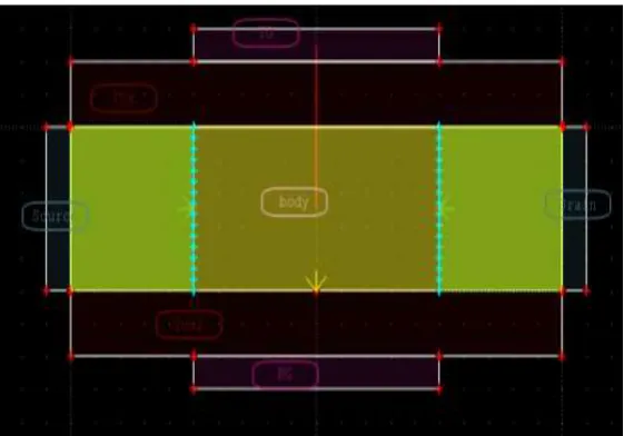
[image:4.595.172.428.237.315.2]In order to design a 10 nm Double gate MOSFET. It is important to make its geometry first in which various regions are well defined like source, drain, gate, body, Oxide. The doping is done in the source, drain and substrate regions. The materials of these regions are given in the table I below .while the Table 2 shows various parameters and there values that we use in this device.
Table -1: Regions and materials used in MOSFET
Region Material
Source/drain Al
Substrate Silicon
Gate n-poly Si
Oxide SiO2
[image:4.595.170.424.349.454.2]
Table -2: Parameters and their values of MOSFET
Parameter Length/T
hickness Mesh conc. Size/Doping Gate length 10 nm Mesh size=.01
Parameter 20nm Mesh size=.005 1 1015cm-3(acceptor)
Source/drain 5nm 1 1021cm-3(donor)
Oxide(SiO2) 2nm Mesh size=.01
Design and Simulations
To design the 10 nm Double Gate MOSFET we make use of Visual TCAD tool which is device simulation tool. The geometry of DG MOSFET is shown below in Figure 5.The mesh file obtained is shown in Figure 6
[image:4.595.158.439.518.714.2]© 2019, IRJET | Impact Factor value: 7.211 | ISO 9001:2008 Certified Journal
| Page 1326
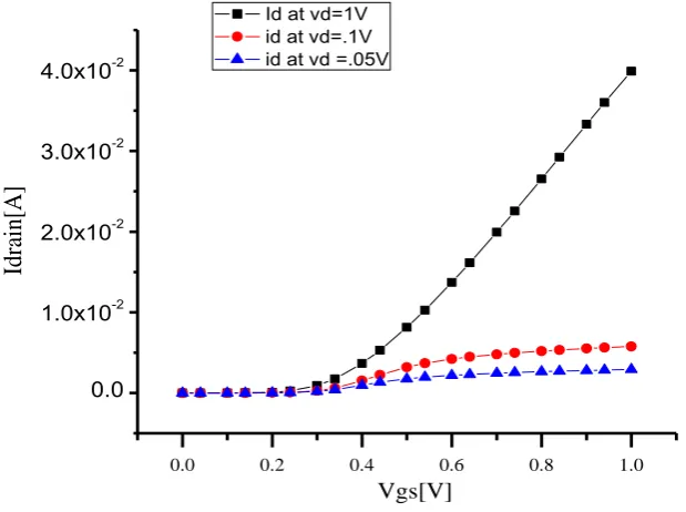
Figure 6: Material structure of 10 nm DG MOSFETOnce the simulations are done we obtain the Id-Vg plot shown in Figure 7. From Id and vg graph we can easily obtain
threshold voltage (Vth).it is the voltage at which channel is created. The drain voltage is taken as .05 V and the gate voltage
is varied from 0v to 1v with start voltage equal to 0V and stop voltage equal to 1V with a voltage sweep of .01v. Figure 7 shows Id -vg plot. It is clear from Figure 7 that the value of drain current Id increases after the Vth .These curves are
obtained by using Genius simulator of Visual TCAD tool.
0.0 0.2 0.4 0.6 0.8 1.0
0.0
1.0x10⁻²
2.0x10⁻²
3.0x10⁻²
4.0x10⁻²
Id at vd=1V id at vd=.1V id at vd =.05V
Vgs[V]
Idrain[A]
Figure 7: Id-Vgs plot of 10 nm DG MOSFET
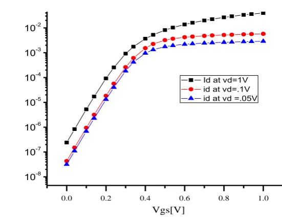
In order to obtain Ion and Ioff value, the transfer characteristics curve plotted between Id and Vgs are shown Figure 8. From
© 2019, IRJET | Impact Factor value: 7.211 | ISO 9001:2008 Certified Journal
| Page 1327
0.0 0.2 0.4 0.6 0.8 1.0
10-8
10-7
10-6
10-5
10-4
10-3
10-2
Id at vd=1V id at vd=.1V id at vd =.05V
Vgs[V]
[image:6.595.143.419.91.308.2]Idrain[A]
Figure 8: Transfer characteristics of MOSFET
Also we can obtain a plot between Id and Vds .In this the Vgs is kept constant where the Vds is varied with start voltage equal
to 0v and stop voltage equal 1v having voltage step of .1V.From the Id vs Vd curve we can obtain value of transconductance
.Figure 9 Shows Id-Vds plot of DG MOSFET.
0.0 0.2 0.4 0.6 0.8 1.0
0.0
1.0x10⁻²
2.0x10⁻²
3.0x10⁻²
4.0x10⁻²
ID at Vg=1V ID at Vg=.3V
Vdrain[V]
[image:6.595.61.530.385.798.2]Idrain[A]
Figure 9: Id –Vd curve of DG MOSFET.
The Simulation results of 10nm Double gate MOSFET are shown in Table 3.
Table 3: Simulation Results of MOSFET
VDD 1v
Vth(V) .22v
Leakage current(Ioff) 3.05×10⁻⁸ A
Drain current(Ion) 3.02×10⁻³ A
Ion/Ioff 9.9×10⁴
DIBL 69.6 mV/V
Transconductance 2.7 ×10⁻² Ω-1
[image:6.595.139.438.392.574.2]© 2019, IRJET | Impact Factor value: 7.211 | ISO 9001:2008 Certified Journal
| Page 1328
3. CONCLUSION10 nm Double gate mosfet is designed and analyzed on Visual Tcad tool in terms of I-V characteristics. From the simulation results of 10 nm Double gate it gives 0.22V threshold voltage at Vdd of 1V.Using an additional gate, the DIBL is reduced to 69.6mV/V. The leakage current of 3.05×10⁻⁸ A is observed due to which Ion/Ioff factor is improved to a greater extent. An
optimum value of subthreshold slope is observed. These improved parameters suggested that the device designed at such dimension is very important for reducing short channel effects. A Visual TCAD is used which makes of drift diffusion model for transportation of carriers.
REFERENCES
[1] Scott E. Thompson and Srivatsan Parthasarathy “Moore’s law: the future of Si microelectronics”, SWAMP Center, Department of Electrical and Computer Engineering, University of Florida, Gainesville, FL
[2]"1965 – "Moore's Law" Predicts the Future of Integrated Circuits". Computer History Museum.
[3] Neetu, Sumit Choudhary, B. Prasad, “Simulation of Double Gate MOSFET at 32 nm Technology Node Using Visual TCAD TM Tool,” Advanced Research in Electrical and Electronic Engineering, Volume 1, Number 4 (2014) pp. 9-13
[4] K. Suzuki, “Scaling theory for double-gate SOI MOSFET’s,” IEEE Trans. Electron Devices, vol. 40, pp. 2326–2329, 1993.
[5] Digh Hisamoto, IEEE transactions on electron devices, vol. 47, no. 12, December 2000.
[6] H.-S. Wong, D. Frank, and P. Solomon, “Device Design Considerations for Double-Gate, Ground-Plane, and Single- Gated Ultra-Thin SOI MOSFET’s at the 25 nm Channel Length Generation,” IEDM Tech. Digest, p. 407 (1998).
[7] Yang, C. Vieri, A. Chandrakasan, and D. Antoniadis, “Back- Gated CMOS on SOIAS for Dynamic Threshold Voltage Control,” IEEE Trans. Electron Devices 44, 822(1997).
[8] Leland Chang, Stephen Tang, “Gate Length Scaling and Threshold Voltage Control of Double-Gate MOSFETs’’Department of Electrical Engineering and Computer Sciences, University of California, Berkeley, CA 94720, USA.
[9] H.S.P Wong. “Beyond the conventional transistor”, Solid-State Electronics, 49, (2005), pp. 755-762.
[10] C. Fiegna, “A new scaling methodology for the 0.1–0.025 um MOSFET,” in VLSI Symp. Tech. Dig., 1993, pp. 33–34.
[11] Jean-Pierre Colinge, “Silicon on Insulator Technology” Springer (2008)
[12] B. Majkusiak, T. Janik, and J. Walczak, “Semiconductor thickness effects in the double-gate SOI MOSFET,” IEEE Trans. Electron Devices, vol. 45, pp. 1127–1134, May 1998.
[13] H. S. Wong, D. J. Frank, Y. Taur, and J. M. C. Stork, “Design and performance considerations for sub-0.1 um double-gate SOI MOSFET’s,” in IEDM Tech. Dig., 1994, pp. 747–750
[14] Kaushik Roy, Kiat Seng Yeo, “Low Voltage, Low Power VLSI Subsystems”, McGraw-Hill Professional, 2004, pp. 4 & 44
![Figure 1:Moore’s law[2]](https://thumb-us.123doks.com/thumbv2/123dok_us/9331993.435203/1.595.115.479.430.703/figure-moore-s-law.webp)
![Figure 3: Symmetrical DG MOSFET [3]](https://thumb-us.123doks.com/thumbv2/123dok_us/9331993.435203/2.595.117.465.163.392/figure-symmetrical-dg-mosfet.webp)
![Figure 4: Asymmetrical DG MOSFET [3]](https://thumb-us.123doks.com/thumbv2/123dok_us/9331993.435203/3.595.170.429.152.253/figure-asymmetrical-dg-mosfet.webp)