Transistor Implementation of Reversible
Comparator Circuit Using Low Power Technique
Madhina Basha , V.N.Lakshmana Kumar Department of ECE, MVGR COLLEGE OF ENGINEERING
Visakhapatnam, A.P, INDIA
Abstract: Reversible logic has emerged as one of the most
important approaches for power optimization with its application in low power VLSI design. Reversible or information lossless circuits have applications in nanotechnology, digital signal processing, communication, computer graphics and cryptography. They are also a fundamental requirement in the emerging field of quantum computing. This paper presents a novel design of reversible arithmetic circuits using existing reversible gates and proposed new reversible gates. The reversible gates are evaluated in terms of number of transistor count, critical path, garbage outputs and one to one mapping. Here transistor implementation of the reversible gates is done by using a combination CMOS-GDI circuit which provides the optimal solution for combinational logic, saving 1/3 the power, half the area and 10% in delay relative to a CMOS implementation. GDI circuits provide some measure of enhanced hazard tolerance and are more suitable for low voltage operation. Here transistor implementation of reversible gates is done by using Tanner tools and H-spice tools.
Keywords: Reversible Gates, Gate Diffusion Input (GDI), Comparator.
I. INTRODUCTION
Conventional combinational logic circuits dissipate heat for every bit of information that is lost during their operation. Due to this fact the information once lost cannot be recovered in any way. But the same circuit if it is constructed using the reversible logic gates will allow the recovery of the information. In 1960s R.Landauer demonstrated that even with high technology circuits and systems constructed using irreversible hardware, results in energy dissipation due to information loss [1].He showed that the loss of one bit of information dissipates KTln2 joules of energy where K=1.3806505*10-23m2kgs-2K-1 is Boltzmann’s constant and T is the temperature where the operation performed. [1]. Later Bennett, in 1973, showed that these KTln2 joules of energy dissipation in a circuit can be avoided if it is constructed using reversible logic circuits [2].
A reversible logic gate is an n-input, n-output logic device with one-to-one mapping. This helps to determine the outputs from the inputs but also the inputs can be uniquely recovered from the outputs. Extra inputs or outputs are added so that the number of inputs is made equal to the number of outputs whenever it is necessary. An important constraint present on the design of a reversible logic circuit using reversible logic gate is that fan-out is not allowed. A reversible circuit should be designed using minimum number of reversible gates. One key requirement to achieve optimization is that the designed circuit must
produce minimum number of garbage outputs. Also they must use minimum number of constant inputs [3, 4].
In this paper, the discussion is made on the Novel reversible comparator circuits and a Novel Optimized Reversible Logic Gates with minimal number of garbage bits, transistor count and unit delay is proposed. In this transistor implementations of Reversible Logic Gates are done by using GDI method [5, 6].
II. BASIC REVERSIBLE LOGIC GATES
A. Reversible Logic Gate
A logic gate L is reversible if, for any output y, there is a unique input x such that,
L(x) = y
If a gate L is reversible, there is an inverse gate L’ which maps y to x for which
L’(y) = x
It is an n-input n-output logic function in which there is a one-to-one correspondence between the inputs and the outputs. Because of this bijective mapping the input vector can be uniquely determined from the output vector. This prevents the loss of information which is the root cause of power dissipation in irreversible logic circuits. In the design of reversible logic circuits the following points must be considered to achieve an optimized circuit. They are
Fan-out is not permitted.
Loops or feedbacks are not permitted. Garbage outputs must be minimum Minimum delay.
Minimum quantum cost.
B. Basic Reversible Logic Gates
Some of the important basic reversible logic gates are, Feynman gate [7], Fredkin gate [4] and Toffoli gate [3], Peres gate [8], R- gate [9], TR gate.
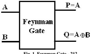
1) Feynman / CNOT Gate:
Fig 1 shows the Feynman gate which is a 2*2 gate and is also called as Controlled NOT and it is widely used for fan-out purposes. The inputs (A, B) and outputs P=A, Q= AB. It has Quantum cost one.
2) Peres Gate:
Fig 2 shows a Peres gate which is a 3*3 gate having inputs (A, B, C) and outputs P = A, Q = AB, R = ABC. It has Quantum cost four.
Fig 2. Peres Gate – 3*3
3) Toffoli Gate:
Fig 3 shows a Toffoli gate which is a 3*3 gate with inputs (A, B, C) and outputs P=A, Q=B, R=ABC. It has Quantum cost five.
Fig 3. Toffoli Gate – 3*3
4) Fredkin Gate:
Fig 4 shows a Fredkin gate which is a 3*3 gate with inputs (A, B, C) and outputs P=A, Q=AB+AC, R=AB+AC. It has Quantum cost five.
Fig 4. Fredkin Gate – 4*4
5) TR Gate:
Fig 5 shows a 3*3 gate with inputs (A, B, C) and outputs P=A, Q=AB, R= ABC. It has Quantum cost six.
Fig 5. TR Gate – 3*3
6) BJN Gate:
Fig 6 shows a BJN Gate which is a 3*3 gate with inputs (A,B,C) and outputs P=A, Q=B, R=(A+B)C. It has Quantum cost five.
Fig 6. BJN Gate – 3*3
7) Proposed M Gate :
The logic diagram and truth table of the proposed new Reversible M gate is as shown in the Fig 7 and Table 1. M Gate which is a 3*3 gate with inputs (A, B, C) and outputs P=A, Q= (AB), R= AB C.
Fig 7. M Gate-3*3
TABLE 1. Truth table of M gate A B C P Q R 0 0 0 0 1 0 0 0 1 0 1 1 0 1 0 0 0 0 0 1 1 0 0 1 1 0 0 1 0 1 1 0 1 1 0 0 1 1 0 1 1 0 1 1 1 1 1 1
8) Proposed L Gate :
The logic diagram and truth table of the proposed new Reversible L gate is as shown in the Fig 8 and Table 2. L Gate which is a 3*3 gate with inputs (A, B, C) and outputs P=A, Q=B, R= (A+B) C.
Fig 8. L Gate – 3*3
TABLE 2. Truth table of L gate
A B C P Q R 0 0 0 0 0 1 0 0 1 0 0 0 0 1 0 0 1 0 0 1 1 0 1 1 1 0 0 1 0 0 1 0 1 1 0 1 1 1 0 1 1 0 1 1 1 1 1 1
III. TRANSISTOR IMPLEMENTATION OFLOGIC GATE USING GDI METHOD.
A. GDI as Alternative Circuit Methodology
The GDI method [5] is based on the use of a simple cell as shown in Fig. 9. At a first glance the basic cell resembles the standard CMOS inverter, but there are some important differences, GDI cell contains three inputs - G (the common gate input of the nMOS and pMOS transistors), P (input to the outer diffusion node of the pMOS transistor) and N (input to the outer diffusion node of the nMOS transistor). The Out node (the common diffusion of both transistors) may be used as input or output port, depending on the circuit structure.
Fig 9. GDI basic cell
Table 3 shows how a simple change of the input configuration of the simple GDI cell corresponds to very different Boolean functions. Most of these functions require a complex (6-12 transistors) gate in CMOS (as well as in standard PTL implementations), but are very simple (only two transistors per function) in the GDI design methodology. GDI enables simpler gates, lower transistor count, and lower power dissipation.
TABLE 3
Some logic functions that can be implemented with a single GDI cell
N P G OUT FUNCTION
0 B A AB F1
B 1 A A+B F2
1 B A A+B OR
B 0 A AB AND
C B A AB+AC MUX
0 1 A A NOT
Multiple-input gates can be implemented by combining several GDI cells. The buffering constrains, due to possible VT drop are described in detail in [10], as well as the technological compatibility with CMOS (and with SOI).
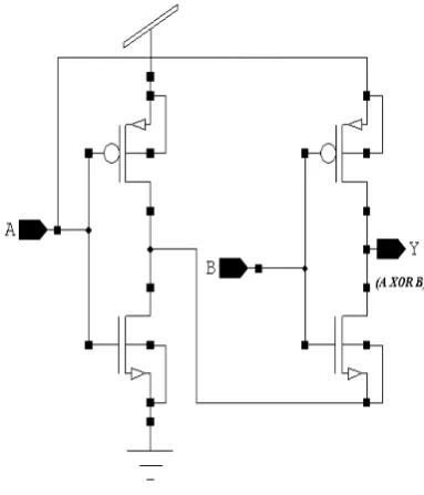
1) Design of XOR gate
The design of XOR gate is shown in Fig 10. The design is based on GDI method. Here two GDI cells are considered in which one cell in taken as basic inverter and for the
second cell A input given to P, B input is given to G and output of first cell is given to N.
Fig 10.XOR gate using GDI
2) Design of OR gate
The design of OR gate is shown in Fig 11. To make the basic GDI cell to work as OR gate input B is given to P, input A is given to G, and VDD is given to N.
Fig 11.OR gate using GDI
B. Transistor implementation of proposed Reversible gates.
In this paper two new reversible gates are proposed. The main intension is to implement the reversible comparator with minimal number of reversible gates, transistor count, and garbage bits.
1) Proposed Reversible M gate
Fig 12. Transistor implementation of proposed M gate
2) Proposed Reversible L gate
The L gate takes A, B, C as inputs and Produce P, Q, R as outputs and corresponding functionalities shown in Fig.8. The transistor implementation of L gate using GDI is shown in Fig13.
Fig 13. Transistor implementation of proposed L gate
IV. DESIGN OF ONE - BIT COMPARATOR
A. Implementation of One-bit Irreversible Comparator.
The conventional one-bit irreversible numerical comparator, which consists of two NOT gates, two AND gates and one NOR gate [11], is shown in Fig.14 with its truth table in Table 4. We can get the following logic expressions from Table 4.
Fig. 14 Irreversible gates for Numerical comparator TABLE 4.Truth table of 1- bit comparator
Input Out put
A B FA>B FA<B F A=B
0 0 0 0 1
0 1 0 1 0
1 0 1 0 0
1 1 0 0 1
B. Implementation of One-Bit Reversible Comparator. 1) One bit comparator using Fredkin and BJN gate
Reversible one bit comparator is implemented with Feynman gate and Fredkin gate and BJN gate is as shown in fig.15. The number of garbage outputs are six and represented with G1 to G6, it uses seven constant inputs, four logic ‘0’ and three logic ‘1’. Two Feynman gates are used for fan-out purpose in the input part [11].
Fig.15. one bit comparator using Fredkin gate
2) One bit comparator using Toffoli and BJN gate
Reversible one bit comparator is implemented with Feynman gate and Toffoli gate as shown in fig.16. the number of garbage outputs are two and represented as G1 and G2 it uses three constant inputs, one logic ‘0’ and two login ‘1’ it requires one Feynman gate and two Toffoli gates[11].
Fig.16. one bit comparator using Toffoli gate
3) One- bit comparator using Peres and BJN gate
Reversible one bit comparator is implemented with Feynman gate and Peres gate and BJN gate as shown in fig.17. The number of garbage outputs are two and represented as G1 and G2, it uses three constant inputs one logic ‘0’ and two logic ‘1’[11].
Fig.17. one bit comparator using Peres gate
4) One- bit comparator using proposed M and L gates.
Reversible one bit comparator is implemented with M gate and L gate as shown in fig.18. The number of garbage outputs is one and represented as G, it uses two constant inputs as logic ‘0’.
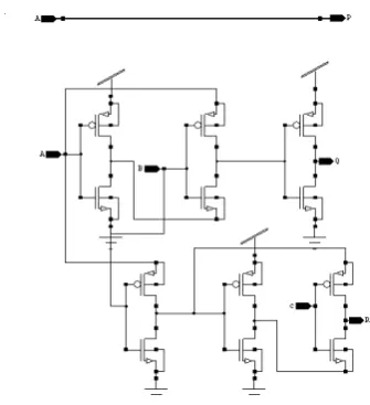
V. TRANSISTOR IMPLEMENTATION OF PROPOSED ONE-BIT COMPARATOR
USING GDI METHOD.
Comparator circuit can be implemented with different combinations of XOR/XNOR modules and AND modules using different CMOS approaches but this approach has not been used in current work. Proposed comparator circuit has been implemented by Reversible gates which are designed using GDI cells as shown in Fig 18. The one-bit comparator using proposed gates with 18 transistors has been implemented as shown in Fig 19. The typical values of width (Wn & Wp) 1.0µm & 2.0µm for nMOS and pMOS transistors have been taken with gate length of 0.18µm. Simulation have been performed using spice based on 0.18µm CMOS technology with supply voltage of 5V.
Fig.19. Transistor implementation of proposed one-bit comparator
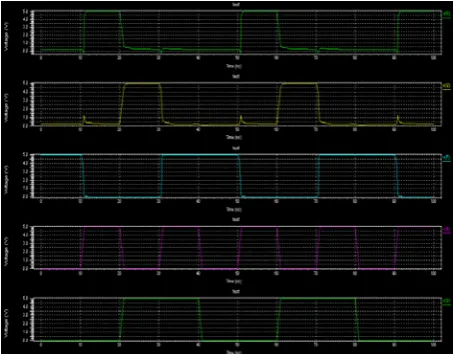
VI. RESULTS
The proposed one-bit comparator using M and L gates are realized using tanner and H spice tools to simulate the output. The simulations are performed using the 0.18µm technology. The input and output waveforms are depicted in Fig 20. The comparative study on the existing one-bit comparator and the proposed one-bit comparator are depicted in the Table 5.
Fig.20. Input and Output waveforms of 1-bit comparator
TABLE.5. Comparison results
One big comparator design using
Reversible gates
Garbage outputs
Constant inputs
Fredkin and BJN 5 6 7
Toffoli and BJN 4 2 3
Peres and BJN 3 2 3
Proposed M and L
gates 2 1 2
Chart 1 shows the graphical representation of Table 5.
0
0.5
1
1.5
2
2.5
3
3.5
4
4.5
Peres
Toffoli
R and
M and
Revers
Garba
Consta
Chart1. Comparison results
Table 6 shows the transistor count, power dissipation, surface area for one-bit comparator between conventional CMOS and GDI method. Proposed one-bit comparator made of GDI cells (Fig 19) shows power dissipation of 0.315mWatt with the input voltage of 5v. Power dissipation and surface area is calculated using micro wind tool.
TABLE.6. Comparison results Proposed
one bit comparator design using
Transistor count
Power dissipation
vdd(5V) power(mWatt)
Surface Area (µm2)
CMOS 50 1.715 3430.7
GDI 18 0.315 982.1
VII. CONCLUSION
In this paper an optimized reversible comparator is presented with the proposed new Reversible M and L gates. The design is very useful for the future computing techniques like ultra low power digital circuits and quantum computers. It is shown that the proposal is highly optimized in terms of number of reversible logic gates, number of garbage outputs, number of constant inputs and number of transistor count.
REFERENCES
[1] R.Landauer, “Irreversibility and Heat Generation in the
Computational Process”, IBM Journal of Research and
Development, 5, pp.183- 191, 1961.
[2] C.H. Bennett, “Logical Reversibility of Computation”, IBM J.Research and Development, pp. 525-532, November 1973.
[3] T.Toffoli., “Reversible Computing”, Tech memo MIT/LCS/TM-151, MIT Lab for Computer Science 1980.
[4] E.Fredkin and T. Toffoli, “Conservative logic,” Int’l J. Theoretical Physics, Vol. 21, pp.219–253, 1982.
[5] Arkadiy Morgenshtein, Michael Moreinis and Ran Ginosar, ”Asynchronous Gate-Diffusion-Input (GDI) Circuits” Very Large Scale Integration (VLSI) Systems, IEEE Journal Transactions, Aug. 2004.
[6] A. Morgenshtein, A. Fish, I. A. Wagner, “Gate-Diffusion Input (GDI) – A Novel Power Efficient Method for Digital Circuits: A Detailed Methodology,” 14th IEEE International ASIC/SOC Conference, USA, September 2001.
[7] R. Feynman, “Quantum Mechanical Computers,” Optics News, Vol.11, pp. 11–20, 1985.
[8] Peres, “Reversible Logic and Quantum Computers”, Physical review A, 32:3266- 3276, 1985.
[9] D.P.Vasudevan, P.K.Lala, J.Di and J.P.Parkerson, “Reversible-logic design with online testability”, IEEE Trans. On Instrumentation and Measurement, vol.55, no.2, pp.406- 414, April 2006.
[10] A. Morgenshtein, A. Fish, I. A. Wagner, “Gate-Diffusion Input (GDI) – A Power Efficient Method for Digital Combinatorial Circuits,” to be published, IEEE Trans., on VLSI.