ISSN (Print) : 2320 – 3765 ISSN (Online): 2278 – 8875
I
nternational
J
ournal of
A
dvanced
R
esearch in
E
lectrical,
E
lectronics and
I
nstrumentation
E
ngineering
(An ISO 3297: 2007 Certified Organization)
Vol. 5, Issue 12, December 2016
Design of 15T SRAM Bit Cell in 180nm
Technology Using Cadence Tool
Dr.David Solomon George
1,
Athira Shanmughan A
2Associate Professor, Dept. of ECE, Government Engineering College, Idukki, Kerala, India1 PG Student [VLSI & ES], Dept. of ECE, Government Engineering College, Idukki, Kerala, India2
ABSTRACT: SRAM can be found in the cache memory of a computer or as a part of the RAM digital to analog converter on a video card. Static RAM is also used for high-speed registers, caches and small memory banks like a frame buffer on a display adapter. The SRAM consist of bitcell,conventional SRAM of 6T bitcell.the design process with conventional, then 13T SRAM cell with dual feedback method. Stack approach is a leakage power reduction technique, which forces a stack effect.Using stacking effect to the two inverters in the cell and designed 15T SRAM with reduced leakage current and delay.
KEYWORDS: Stacking effect
I.INTRODUCTION
Now days with the growth the rapid growth of communication and signal processing the electronics became aware to the consumer. So the designer need substantial cost and form factor reduction system. So the designer brings SOC (system on chip) Designing system. In which the 70% of area of SOC is being covered by the SRAM cell which needs low power for the operation. And the speed of operation is also high which is so demand in the now days market. So we need for the design of the SRAM kind memory cell in the market. Although there is some need of powerful design of the powerful operation for this. SRAM,static RAM or static random access memory is an improvement upon DRAM.DRAM is compressed of a capacitor and a transistor which require information to be periodically(or refreshed) for data to remain valid.SRAM memory on the other hand ,does not need to be refreshed at all.static RAM maintains its information long as the chip has a enough power to keep in data.the reason is because SRAM chips are made of flip-flop circuit which does not need constant refreshing.another benefit to static random access memory is very fast access speed, much faster than DRAM.the reason behind the speed is a configuration of six transistors which keep current flowing in one direction or the other(0 or 1) .each state can be written and read instantly ,and the chip does not require a capacitor to fill up or drain.SRAM can be found in the cache memory of a computer or as a part of the RAM digital to analog converter on a video card. Static RAM is also used for high-speed registers,caches and small memory banks like a frame buffer on a display adapter. Several scientific and industrial subsystems,modern applications, automotive electronics, electronic toys,mobile phones, space applications, synthesizers and digital cameras also use SRAM.It is also highly recommended for use in PCs, peripheral equipment,printers,LCD screens, hard disk buffers, router buffers and buffers in CDROM/CDRWdrivers.
ISSN (Print) : 2320 – 3765 ISSN (Online): 2278 – 8875
I
nternational
J
ournal of
A
dvanced
R
esearch in
E
lectrical,
E
lectronics and
I
nstrumentation
E
ngineering
(An ISO 3297: 2007 Certified Organization)
Vol. 5, Issue 12, December 2016
most efficient way to achieve ULP operation in integrated energy. When the particle hits a reverse-biased p-n-junction, such as a transistor diffusion-bulk junction, the injected charge is transported by drift and causes a transient current pulse that changes the node voltage[2]. SRAM cell indicate that, in some cases, more charge can be collected at sensitive nodes fromstrikes that do not cause upset than from strikes that do cause upset. Computations of critical charge must take into account the time during which charge is collected, not simply the total amount of charge collected simply the total amount of charge collected[4],[6].
Low-voltage operation for memories is attractive because of lower leakage power and active energy, but the challenges of SRAM design tend to increase at lower voltage.the limits of low-voltage operation for traditional sixtransistor (6T) SRAM and proposes an alternative bitcell that functions to much lower voltages[1]. Measurements confirm that a SRAM test chip using the proposed bitcell operatesinto sub-threshold to below 400 mV. At this low voltage, the memory offers substantial power and energy savings at the cost of speed, making it well-suited to energy constrained applications[7],[8]. energy minimization for circuits operating in the subthreshold region. Subthreshold operation is emerging as an energy-saving approach to many energy constrained applications where processor speed is less important.solve equations for total energy to provide an analytical solution for the optimum VDD and VT to minimize energy for a given frequency in subthreshold operation. the dependence of the optimum VDD for a given technology on design characteristics and operating conditions. also examines the effect of sizing on energy consumption for subthreshold circuits. minimum sized devices are theoretically optimal for reducing energy. A fabricated 0.18mm test chip is used to compare normal sizing and sizing to minimize operational VDD and to verify the energy models. Measurements show that existing standard cell libraries offer a good solution for minimizing energy in subthreshold circuits[9]-[13].
II.EXISTING SYSTEM
Power dissipation is one of the most important aspects of current nanoscale VLSI design. Ultralow power (ULP) operation is of particular importance in VLSI chips for space applications, where available energy resources are limited. Future small, low-cost satellites have an even lower power budget, as the total satellite weight is often reduced by restricting the use of heavy batteries and power supplies. The most efficient way to achieve ULP operation in integrated circuits is to aggressively reduce the supply voltage (VDD) and operate all components of the chip in the near-threshold or subthreshold region [7], [3], thereby significantly reducing both static and dynamic power consumption. However, in addition to the well-known challenges of a low-voltage circuit design, such as increased delay, sensitivity to process variations, and temperature fluctuations, low-voltage circuits are much more susceptible to radiation effects than circuits powered at nominal supply voltages [3]. The 13T dual-driven separated-feedback bitcell .a unit cell size that is only 2larger than a standard 6T static random access memory (SRAM) bitcell, implemented in the same 0.18µm CMOS process. 13T SRAM shows high stability under varying voltage and process parameter variations, an outstanding advantage over the conventional 6T SRAM cell. The dual-driven separated-feedback mechanism is implemented, in order to improve the bitcell robustness. SRAM blocks occupy the majority of the chip area and are the primary contributors to leakage power in many modern systems, including those intended for space applications [8][10]. These trends lead to two major conclusions. First, due to their static power consumption, scaling the supply voltage of the SRAM macros is an efficient method to reduce total chip power. Second, the probability of a radiation strike on an SRAM bitcell is relatively high due to the large area that the SRAM core occupies. Therefore, SRAM soft-error mitigation has become essential for robust system design.
A.BITCELL DESIGN
ISSN (Print) : 2320 – 3765 ISSN (Online): 2278 – 8875
I
nternational
J
ournal of
A
dvanced
R
esearch in
E
lectrical,
E
lectronics and
I
nstrumentation
E
ngineering
(An ISO 3297: 2007 Certified Organization)
Vol. 5, Issue 12, December 2016
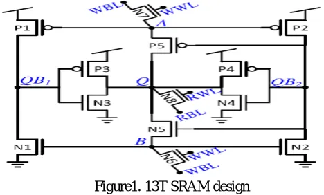
feedback mechanism to overcome the increased vulnerability due to supply voltage scaling. The schematic representation of the 13T bitcell is shown in Figure 1.
Figure1. 13T SRAM design
The storage mechanism of this circuit comprises five separate nodes: Q,QB1, QB2, A, and B, with the acute data value stored at Q. This node is driven by a pair of CMOS inverters made up of transistors N3, P3, N4, and P4 that are, respectively, driven by the inverted data level, stored at QB1 and QB2. QB1 and QB2 are, respectively, driven to VDD or GND through devices P1, P2, N1, and N2 that are controlled by the weak feedback nodes A and B that are connected to Q through a pair of complementary devices (P5 and N5) gated by QB2. By driving the acute data level by a pair of equipotentially driven, but independent, inverters, a strong, dual-driven feedback mechanism is applied with node separation for SEU protection. This setup effectively protects Q from an upset, while achieving a high critical charge at node Q.
B. DESIGN OF 13T SRAM IN 180 NM CMOS TECHNOLOGY
The design of 13T SRAM contain of two inverters.First the inverter is designed with vdd 1.8V linear region. The nmos is set first with the width and length, correspondingly design the pmos.given the input and verify the functioning of the inverter .place the two inverters and other transistors,scale them to linear region of operation. The inverter is designed and simulated,also verify the output.then have to add the other transistors and design the 13T SRAM with VDD 1.8V.transient analysis and obtain the read and write operations.after analysing the transform then design the 13T SRAM with VDD 500mV.
ISSN (Print) : 2320 – 3765 ISSN (Online): 2278 – 8875
I
nternational
J
ournal of
A
dvanced
R
esearch in
E
lectrical,
E
lectronics and
I
nstrumentation
E
ngineering
(An ISO 3297: 2007 Certified Organization)
Vol. 5, Issue 12, December 2016
III.PROPOSED DESIGN
A.STACKING EFFECT
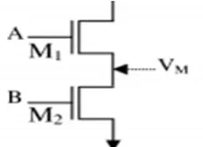
Sub-threshold leakage current that is flowing through a stack of series connected transistors decreases when more than one transistor in the stack is turned off. This effect is known as the stacking effect or self-reverse bias. Leakage currents in NMOS or PMOS transistors depend exponentially on the voltage at the four terminals of transistors. VG is 0 thus increasing VS of NMOS transistor reduces sub-threshold leakage current exponentially. consider a stack of two NMOS transistors.
Fig.3 Effect of transistor stacking on source voltage
When both transistors M1 and M2 are turned off, the voltage at the intermediate node (VM) is positive due to small drain current[5]. Positive potential at the intermediate node has the three following effects: 1) Due to the positive source potential VM, gate to source voltage (VGS1) of transistor M1 becomes negative; hence, the sub-threshold current reduces substantially. 2) Due to VM > 0, body to source potential (VBS1) of transistor M1 becomes negative, which results in an increase in the threshold voltage (larger body effect) of M1, and thus reducing the sub-threshold leakage. 3) Due to VM > 0, the drain to source potential (VDS1) of transistor M1 decreases, which results in an increase in the threshold voltage (less DIBL) of M1 and thus reducing the sub-threshold leakage. If only one NMOS device is off, the voltage at the source node of off transistor would be virtually zero because all other on transistors will act as short circuit. Thus, there is no self reverse biasing effect, and the leakage across the off transistor is large. But if more than one transistor is off, the source voltages of the off transistor, except the one connected to ground by transistors, will be greater than zero, and the leakage will be determined by the most negatively self-reverse biased transistor (because sub-threshold leakage is an exponential function of gate-source voltage). The reverse bias makes the leakage across the off transistor very small.
B.15T SRAM DESIGN
The 15T SRAM bitcell is designed from the 13T SRAM bitcell by stacking two more transistors, stack an nmos to the each inverter.
ISSN (Print) : 2320 – 3765 ISSN (Online): 2278 – 8875
I
nternational
J
ournal of
A
dvanced
R
esearch in
E
lectrical,
E
lectronics and
I
nstrumentation
E
ngineering
(An ISO 3297: 2007 Certified Organization)
Vol. 5, Issue 12, December 2016
1.Write Operation
Standard SRAM topologies, such as the 6T bitcell, write data by driving the new level directly into the storage nodes, and therefore are required to overcome the circuits strong internal feedback..The 15T SRAM cell achieves writes by driving the weak feedback nodes (A and B), thereby removing much of the ratioed contention, inherent to direct access.A pair of write access transistors (N6 and N7) connect a unified write bitline (WBL) to nodes A and B. These devices are controlled by a write wordline (WWL), such that when WWL is raised, A and B are pulled toward the level driven upon WBL. This virtual connection between A and B creates inverters out of the transistor pairs of N1, P1 and N2, P2, driving QB1 and QB2 to the opposite level of WBL. Accordingly, the written data level is driven back to Q through the dual-driven feedback inverters, bringing the cell to a stable state.
2.Read Operation
The 15T bitcell features single-ended readout through the read access transistor (N8). This device is controlled by a separate read wordline and connected to a column-shared read bitline that is precharged prior to the read operation and conditionally discharged, depending on the voltage stored at Q. Due to the dual-driven feedback that drives Q to its stable value, this read operation is both more robust and faster than the read operation of standard SRAM bitcells. Read failures in 6T SRAM cells occur when the access transistor is stronger than the pull-down transistor due to local variations. However, the proposed cell employs a pair of pull-down transistors (N3 and N4), which significantly decrease the probability of such a read failure, enabling robust operation at low voltages. In addition, these two devices also provide a lower resistance pull-down path to achieve a faster bitline discharge. The separated read and write Ports also provide two-ported functionality, often required in memory macros, such as those used for register files.
IV.SIMULATION AND ANALYSIS
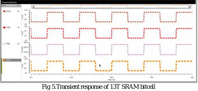
1. Simulation of 13TSRAM bitcell
Transient analysis is done, obtain the read and write operations
Fig 5.Transient response of 13T SRAM bitcell
ISSN (Print) : 2320 – 3765 ISSN (Online): 2278 – 8875
I
nternational
J
ournal of
A
dvanced
R
esearch in
E
lectrical,
E
lectronics and
I
nstrumentation
E
ngineering
(An ISO 3297: 2007 Certified Organization)
Vol. 5, Issue 12, December 2016
2. Simulation of 15T SRAM bitcell
Transient analysis is done, obtain the read and write operations
Fig 6.Transient response of 15T SRAM bitcell
Using cadence tool also obtain the delay=5.76ps, leakage current=17.58nA, SNM(Static Noise Margin)=0.7V. Parameter Value Unit
13T SRAM Average power 18.19 nW Delay 57 ps SNM 1.5 V Leakage current 1.08 µA 15T SARM Average power 3.494 nW Delay 5.467 Ps SNM 1.5 V Leakage current 17.48 nA Table I Comparison of 13T SRAM and 15T SRAM bit cell
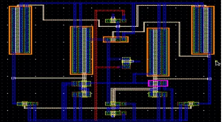
V. LAYOUT STRUCTURE
The Virtuoso Layout Editor is used for drawing the layout. A layout consists of geometrical figures in different colours. From the size and colour of this figures it is later possible to generate the final mask layers which is used in the fabrication of the design. It is possible to include other cells by instanciating their layout views. To verify that the layout fulfills all electrical and geometric rules a Design Rule Check (DRC) program is used. The Assura Diva verification can be called upon directly from the layout editor. This tool will mark any error in the design and can also extract (i.econvert to a netlist) the layout so it can be simulated.
ISSN (Print) : 2320 – 3765 ISSN (Online): 2278 – 8875
I
nternational
J
ournal of
A
dvanced
R
esearch in
E
lectrical,
E
lectronics and
I
nstrumentation
E
ngineering
(An ISO 3297: 2007 Certified Organization)
Vol. 5, Issue 12, December 2016
VI. CONCLUSION
The design and simulate a 15T SRAM bitcell in 180 nm CMOSTechnology at transistor level.stacking nmos transistor to the inverter of 13T SRAM bitcell obtained the design of 15T SRAM.Performance of the bitcells are analysed .15T SRAM bitcell has better read steability.
Future Works
SRAM design for low-voltage operation has become increasingly popular in the recent past. Various bitcell designs and architectural techniques have been proposed to enable operation deep into the subthreshold region.low voltage bitcell can be used for space application.
ACKNOWLEDGMENT
I would like to thank my guide for his support in presenting this thesis. I would also extend my sincere regards to the referees for their comments.
REFERENCES
[1] P. Neil H.E.Weste,David Harris,Ayan Banerjeee ”CMOS VLSI Design A Circuit and Systems Perspective,” Pearson third edition.,
[2] Lior Atias, Adam Teman, Robert Giterman,Pascal Meinerzhagen and Alexander FishA Low-Voltage Radiation-Hardend 13T SRAM Bitcell for Ultralow Power Space Application
IEEE TRANSACTIONS ON VERY LARGE SCALE INTEGRATION (VLSI) SYSTEMS, Feb.2016
[3] S. Fisher, A. Teman, D. Vaysman, A. Gertsman, O. Yadid-Pecht, and A. Fish, Digital subthreshold logic design Motivation and challenges, in Proc. IEEE Conv. Elect. Electron.Eng. Israel (IEEEI, Dec. 2008,pp. 702 706
[4] P. E. Dodd and F. W. Sexton, Critical charge concepts for CMOS SRAMs, IEEE Trans. Nucl. Sci., ,vol. 42, no. 6, pp. 1764 1771,Dec. 1995. [5] Rohit, Gaurav Saini, AStable and Power Efficient SRAM Cell,” IEEE International Conference on Computer, Communication and Control (IC4)., 2015.
[6] L. Sterpone and M. Violante, Analysis of the robustness of the TMR architecture in SRAM-based FPGAs, IEEE Trans. Nucl. Sci., ., vol. 52, no. 5, pp. 15451549, Oct. 2005.
[7] A. Wang, B. H. Calhoun, and A. P. Chandrakasan, Sub-Threshold Design for Ultra Low-Power Systems (Series on Integrated Circuits and Systems). Secaucus, , NJ, USA: Springer-Verlag, 2006.
[8] B. H. Calhoun and A. P.Chandrakasan, A 256-kb 65-nm sub-threshold SRAM design for ultra-low-voltage operation, IEEE J. Solid-State Circuits,vol. 42, no. 3, pp. 680-688, Mar.2007.
[9] B. H. Calhoun, A. Wang, and A. Chandrakasan, Modeling and sizing for minimum energy operation in subthreshold circuits, IEEE J. Solid-State Circuits,. 40, no. 9, pp. 1778-1786, Sep. 2005.
[10] A. Teman, L. Pergament, O. Cohen, and A. Fish, A 250 mV 8 kb 40 nm ultra-low power 9T supply feedback SRAM (SF-SRAM), ), IEEE J. Solid-State Circuits, vol. 46, no. 11,pp. 27132726, Nov. 2011.
[11] J. Mezhibovsky, A. Teman, and A. Fish, Low voltage SRAMs and the scalability of the 9T supply feedback SRAM, in Proc. IEEE Int.Syst.-Chip Conf. (SOCC),Sep. 2011, pp. 136-141.
[12] N. Verma and A. P. Chandrakasan, A 256 kb 65 nm 8T subthreshold SRAM employing sense-amplifier redundancy, IEEE J. Solid-State Circuits,vol. 43, no. 1, pp. 141149, Jan.2008.