DOI: 10.15662/ijareeie.2014.0307065
Analysis of Punch-Through Breakdown Voltages
in 3C-Sic Schottky Barrier Diode Using Gaussian
Profile for 200µm Thick Wafer
Pratibha Nishad1, A. K. Chatterjee2
PG Student (ECE), Department of ECE, Thapar University, Patiala, Punjab, India 1 Professor, Department of ECE, Thapar University, Patiala, Punjab, India2
ABSTRACT: The punch through breakdown voltage of 3C-SiC Schottky Barrier Diode has been analysed in this
paper using Gaussian profile. It is observed that 3C-SiC Schottky barrier diode yield high punch through breakdown voltage with higher values of peak doping concentration and lower values of constant m with increasing depletion region width. So, thinner wafers of 3C-SiC can be used to fabricate Schottky barrier diode to provide higher breakdown voltage using Gaussian profile.
KEYWORDS: 3C-SiC, Schottky Barrier diode, Punch-through breakdown voltage, Gaussian profile
I. INTRODUCTION
Silicon Carbide(SiC) is a wide band gap semiconductor that has energy gap wider than 2eV and has extremely high power, high voltage switching characteristics and high chemical, thermal and mechanical stability. The SiC devices have low mobility which is compensated by its ability to withstand high electric fields taking advantage of the higher carrier velocity. The parameters for the mobility models are collected from measurements for a temperature dependent mobility model [1]. SiC has large band gap, so the intrinsic carrier concentration (responsible for the thermal noise and also partly responsible for the leakage current) is negligible at temperatures up to 600°C. Silicon carbide occurs in many different crystal structures, called polytypes. Despite the fact that all SiC polytypes chemically consist of 50% carbon atoms covalently bonded with 50% silicon atoms, each SiC polytype has its own distinct set of electrical semiconductor properties due to the difference in staking order between the double layers of carbon and silicon atoms[2]. To date, SiC has more than 200 polytypes [3].
II. 3C-SiC SCHOTTKY BARRIER DIODE
Schottky barrier diodes have lower resistance, faster response, and negligible transient reverse current during switching in comparison to p-n rectifiers. Moreover, the reverse saturation current of Schottky diodes is larger than that of p–n junction diodes. Hence, a Schottky diode requires less forward bias voltage to obtain a given current than p–n junction diode. Schottky diodes based on silicon carbide (SiC) are of special importance because of their high voltages and high temperatures handling capacity.
Figure 1 : Cross section of an implant-edge-terminated Schottky barrier diode in SiC [4]
A lightly doped n-type blocking layer is grown on a SiC substrate by chemical vapour deposition. The doping and thickness of the epilayer are selected so that the desired blocking voltage is achieved. On the top surface of the blocking layer an edge termination ring is implanted at the surface and then the Schottky metal is deposited to form Schottky junction. The edge termination ring is required to prevent field crowding at the edge of the metal in the blocking state; otherwise blocking voltage would be significantly reduced. Two types of edge termination rings used are resistive termination extension (RTE) and junction termination extension (JTE).
III. BACKGROUND
German physicist Walter H. Schottky created a theory in 1938 that illustrated the rectifying behaviour of a metal-semiconductor contact as dependent on a barrier layer at the surface of contact between the two materials. Schottky Barrier diodes were later fabricated on the basis of this theory. High voltage Schottky diodes were fabricated on 3C-SiC films grown on Si substrates in 1993. A Ni metallization process was developed to fabricate both rectifying and ohmic contacts to SiC by controlling the post annealing temperature [5]. The characteristics of vertical Schottky barrier diodes (SBD) fabricated on N /N+ 3C-SiC grown on N+Si substrate were reported in 1994[6]. The characteristics of 4H-SiC Schottky barrier diodes were reported in 1995 with breakdown voltages upto 1000 V for the first time [7]. Ni Schottky rectifiers was fabricated on 2.7x1016 cm-3 n-type 6H-SiC epilayer in 2001 using an effective edge termination
based on an oxide ramp profile around the Schottky contact[8]. Silicon Carbide was discussed as energy efficient wide band gap device in 2006 which showed that SiC Schottky diodes allowed up to a 25% reduction in losses in power supplies for computers and servers when used in the power factor correction circuit [9]. The electrical characteristics of Au/3C-SiC Schottky diode was studied as a function of contact area in 2009 [10]. Isothermal and nonisothermal DC characteristics of SiC Schottky barrier diodes were measured in 2010 [11].
HOYA Corporation has succeeded in raising the SiC growth rate to more than 50 times the conventional rate, using a newly developed SiC fabrication process in 2012. With this new process, large monocrystal 3C-SiC substrates (at least 200 micro-meters thick after removing the Si base layer) can be manufactured [12]. An analysis of 4H-SiC power Schottky Barrier Diodes (SBDs) was done in 2013 which showed that these devices can be operated well below their true avalanche breakdown potential [13]. A cost-effective fabrication of Schottky-barrier (SB) diode was proposed in 2014 steering element for low power phase-change memory (PCM) application [14].
The paper is organized as follows: In Section IV, the theoretical analysis is done to study the behaviour of punch through breakdown voltage of 3C-SiC Schottky Barrier Diode using Gaussian profile. The calculations and results are presented in section V. The paper is concluded in section VI.
IV. THEORETICAL ANALYSIS
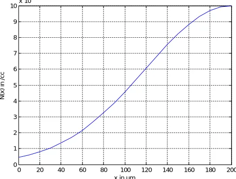
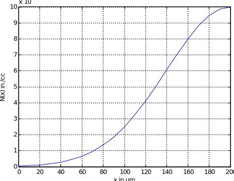
The doping profile used here in Schottky Barrier diode is Gaussian profile. The carrier concentration is maximum at the base of the device decreasing upwards at the contact. The equation to this profile may be written as:
N(x) = N e
1
where, N0 is peak concentration, m is constant, h is the device height (200µm) and x is the distance from the contact.
Here different Gaussian profiles have been generated with different values of peak concentration N0 and constant m. N0
has been varied from 1015 cm-3 to 1018 cm-3.
Figure 2. Profile1-Variation of carrier concentration N(x) with x with peak concentration N0=1015 cm-3 and constant
m=100x10-4cm
Figure 3. Profile2-Variation of carrier concentration N(x) with x with peak concentration N0=1016 cm-3 and constant
m=80x10-4cm
0 20 40 60 80 100 120 140 160 180 200 1
2 3 4 5 6 7 8 9 10x 10
14
x in µm
N
(x
)
in
/
c
c
0 20 40 60 80 100 120 140 160 180 200
0 1 2 3 4 5 6 7 8 9
10x 10
15
x in µm
N
(x
)
in
/
c
Figure 4. Profile3-Variation of carrier concentration N(x) with x with peak concentration N0=10 17
cm-3 and constant m=70x10-4cm
Figure 5. Profile4-Variation of carrier concentration N(x) with x with peak concentration N0=1018 cm-3 and constant
m=60x10-4cm
V. CALCULATIONS AND RESULTS
The equation for calculating depletion region width is given by [15]
−
−
1
−
−
= 0
2
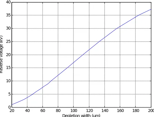
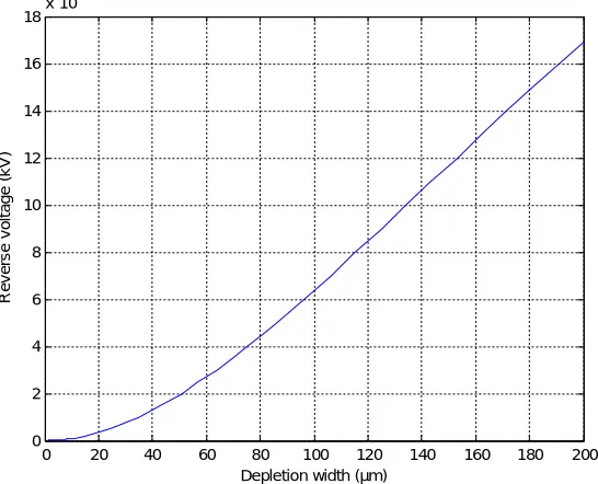
The highest value of reverse voltage VR in above equation at which maximum depletion region width is obtained for a
given value of constant m gives the value of punch through breakdown voltage. The calculations have been done using MATLAB.
Permittivity of 3C-SiC semiconductor, ɛs=9.7 ɛo
Device height, h=200µm
0 20 40 60 80 100 120 140 160 180 200
0 1 2 3 4 5 6 7 8 9
10x 10
16
x in µm
N
(x
)
in
/
c
c
0 20 40 60 80 100 120 140 160 180 200
0 1 2 3 4 5 6 7 8 9
10x 10
17
x in µm
N
(x
)
in
/
c
Figure 6-9 shows the depletion region width calculated for different reverse voltages for the four profiles discussed above.
Figure 6. Variation of reverse voltage with depletion width for profile 1
Figure 7. Variation of reverse voltage with depletion width for profile 2
20 40 60 80 100 120 140 160 180 200 0
5 10 15 20 25 30 35 40
Depletion width (µm)
R
e
v
e
rs
e
v
o
lt
a
g
e
(
k
V
)
0 20 40 60 80 100 120 140 160 180 200
0 100 200 300 400 500 600 700 800
Depletion width (µm)
R
e
v
e
rs
e
v
o
lt
a
g
e
(
k
V
Figure 8. Variation of reverse voltage with depletion width for profile 3
Figure 9. Variation of reverse voltage with depletion width for profile 4
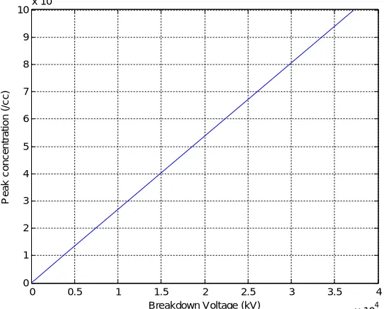
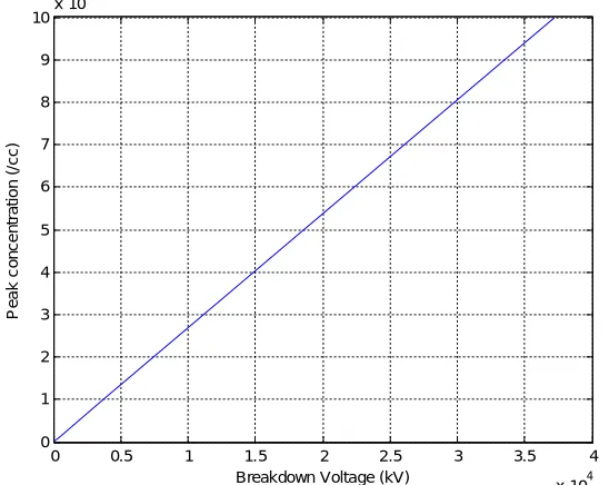
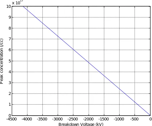
For different values of constant m, breakdown voltage has been calculated for different values of the peak carrier concentration N0 shown in Figures 10-14.
0 20 40 60 80 100 120 140 160 180 200 0
2000 4000 6000 8000 10000 12000
Depletion width (µm)
R
e
v
e
rs
e
v
o
lt
a
g
e
(
k
V
)
0 20 40 60 80 100 120 140 160 180 200
0 2 4 6 8 10 12 14 16 18x 10
4
Depletion width (µm)
R
e
v
e
rs
e
v
o
lt
a
g
e
(
k
V
Figure 10. Variation of breakdown voltage with peak concentration for m=50x10-4 cm
Figure 11. Variation of breakdown voltage with peak concentration for m=100x10-4 cm
0 0.5 1 1.5 2 2.5 3
x 105 0
1 2 3 4 5 6 7 8 9 10x 10
17
Breakdown Voltage (kV)
P
e
a
k
c
o
n
c
e
n
tr
a
ti
o
n
(
/c
c
)
0 0.5 1 1.5 2 2.5 3 3.5 4 x 10⁴ 0
1 2 3 4 5 6 7 8 9 10x 10
17
Breakdown Voltage (kV)
P
e
a
k
c
o
nc
e
nt
ra
ti
on
(
/c
c
Figure 12. Variation of breakdown voltage with peak concentration for m=141x10-4 cm
Figure 13. Variation of breakdown voltage with peak concentration for m=141.4x10⁻⁴ cm
0 50 100 150 200 250
0 1 2 3 4 5 6 7 8 9 10x 10
17
Breakdown Voltage (kV)
P
e
a
k
c
o
n
c
e
n
tr
a
ti
o
n
(
/c
c
)
0 0.5 1 1.5 2 2.5 3 3.5 4 x 10⁴ 0
1 2 3 4 5 6 7 8 9 10x 10
17
Breakdown Voltage (kV)
P
e
a
k
c
o
n
c
e
n
tr
a
ti
o
n
(
/c
c
Figure 14. Variation of breakdown voltage with peak concentration for m=150x10-4 cm
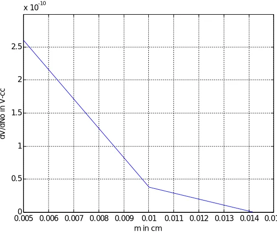
Now, the variation of derivative of breakdown voltage w.r.t. peak concentration with the values of constant m and variation of derivative of depletion width w.r.t. breakdown voltage with peak concentration is studied shown in Figure 15-16.
Figure 15. Variation of gradient of depletion width with breakdown voltage with respect to peak concentration
-45000 -4000 -3500 -3000 -2500 -2000 -1500 -1000 -500 0 1
2 3 4 5 6 7 8 9 10x 10
17
Breakdown Voltage (kV)
P
e
a
k
c
o
n
c
e
n
tr
a
ti
o
n
(
/c
c
)
0 1 2 3 4 5
10^15 10^16 10^17 10^18
d
W
/d
V
(
µ
m
/k
V
)
Figure 16. Variation of gradient of breakdown voltage with peak concentration with respect to constant m
An analysis of the Figures 6-9 shows that the magnitude of gradient of depletion region width with breakdown voltage is found to decrease for the Gaussian profiles considered in this study which is shown in Figure 15. So, it means that with an increase in N0 associated with decrease in m gives rise to an increase in breakdown voltage with an increase in
depletion region width.
The sequence of plots of N0 against VB for 200µm thick device of 3C-SiC Schottky Barrier Diode for increasing values
of m ranging from m=50x10-4cm to 150x10-4cm are shown in figure 10-14. An analysis of these curves shown in Figure 16 shows that at over a range of values of N0, if we consider the variation of breakdown voltage, it is seen that
the variation of breakdown voltage with N0 is found to increase with decreasing value of m. VI. CONCLUSION
The present study which has been used to analyse punch through breakdown voltage of 3C-SiC Schottky Barrier Diode have been done based on using Gaussian profiles in semiconductor region of these devices. The analysis showsthat an increase in N0 with a decrease in m gives rise to an increase in breakdown voltage with increasing depletion region
width.
ACKNOWLEDGEMENT
We would like to sincerely thank the ECE department of Thapar University, Patiala for their continuous support and guidance during the course of this work.
REFERENCES
[1] M. Roschke, F. Schwiertz, “Electron mobility Models for 4H, 6H, and 3C SiC”, IEEE trans. Elec. Dev. Vol. 48, No. 7, 2001, pp.1442-1447.
[2] G. R. Fisher and P. Barnes, ―Towards a Unified View of Polytypism in Silicon Carbideǁ, Philosophical Magazine, vol. 61, pp. 217-236, 1990.
[3] O. Kordina, ―Growth and Characterisation of Silicon Carbide Power Device Material, PhD thesis, Lonkoping University, 1994.
[4] Munish Vashishath and Ashoke K. Chatterjee, “Recent trends in silicon carbide device research”, Mj. Int. J. Sci. Tech., 2(03). Pp. 444-470, 2008.
0.005 0.006 0.007 0.008 0.0090 0.01 0.011 0.012 0.013 0.014 0.015
0.5 1 1.5 2 2.5
x 10-10
m in cm
d
V
/d
N
o
i
n
V
-c
[5] A. J. Steckl and J. N. Su, ”High Voltage Temperature-Hard 3C-SiC Schottky Diodes Using All-Ni Metallization”, IEEE Trans. Electronics Device, pp 695-698, 1993.
[6] Praveen Shenoy, Akira Moki, B.J.Baliga, Dev Alok, K.Wongchotigul and M.Spencer, ” Vertical Schottky Barrier Diodes on 3C-Sic Grown on Si”, IEEE Trans. Electronics Device, pp 411-414, 1994.
[7] R. Raghunathan, D. Alok, and B. J. Baliga―High Performance of High- Voltage 4H-SiC Schottky Barrier Diodesǁ, IEEE Electron Device Letters, vol. 16, pp. 280-282, 1995.
[8] Gheorghe Brezeanu, Marian Badila, Bogdan Tudor, José Millan,Philippe Godignon, Florin Udrea, G. A. J. Amaratunga and Andrei Mihaila,” Accurate Modeling and Parameter Extraction for 6H-SiC Schottky Barrier Diodes (SBDs) With Nearly Ideal Breakdown Voltage”, IEEE Transactions on Electron Devices, Vol. 48, NO. 9, 2001.
[9] J.W. Palmour, ―Energy Efficient Wide Bandgap Devicesǁ, Compound Semiconductor IC Symposium, pp. 4-7, 2006.
[10] Jens Eriksson, Ming Hung Weng, Fabrizio Roccaforte, Filippo Giannazzo, Stefano Leone,Vito Raineri, “Toward an ideal Schottky barrier on 3C-SiC”, Applied Physics Letters, vol. 95, 2009.
[11] W. Janke, A. Hapka, -The current-voltage characteristics of SiC Schottky barrier diodes with the self-heating included, Koszalin University of Technology, Poland, 2010.
[12] Press conference, HOYA Corporation, Mono-crystal 3C-SiC large size substrate, Japan, 2012. [13] K. Shenai, “Optimization of 4H-SiC Power Schottky Barrier Diodes”, IEEE Energytech, 2013.
[14] Yan Liu, Chao Zhang, Zhitang Song, Bo Liu, Guanping Wu, Jia Xu, Lianhong Wang, Lei Wang, Zuoya Yang, and Songlin Feng, “Cost-Effective Schottky-Barrier Diode Array with Ni–Silicidation Accessing Low Power Phase-Change Memory”, IEEE Transactions on Electron Devices, Vol. 61, No. 3, 2014.
[15] Munish Vashishath, “Analysis and Design of Robust Power Double Implanted MOSFET on 6H silicon carbide wafers”, Doctoral Thesis, Thapar University, 2010.
Rishikesh Pandey is presently