IJEDR1604100
International Journal of Engineering Development and Research (www.ijedr.org)663
Simulation and Analysis of CNTFETs based Logic
Gates in HSPICE
1
Neetu Sardana,
2L.K. Ragha
1M.E Student,
2Guide
1Electronics Department,
1Terna Engineering College, Navi Mumbai, India
________________________________________________________________________________________________________
Abstract—Conventional CMOS technology provides a lot of opportunities in the field of electronic devices. After the
invention of the MOSFET, continuous scaling of the device is going on as predicted by Moore in 1970. This reduction in device size is giving higher performance in terms of increased speed, lower power consumption at lower cost with greater chip density. The main disadvantage of scaling is channel length is also decreasing continuously leading to short channel effects(SCE) in nanoscales regime. To overcome these limitations many alternate devices are proposed. Among these various alternate devices, Carbon Nano Tube Field Effect Transistor (CNTFET) is found to be one of the most promising alternatives for MOSFET. The CNTFET is a field effect transistor in which Carbon Nano Tube(CNT) is used in the channel region. In this paper the standard model has been designed for, MOSFET like CNTFET devices. Various logic gates were designed using CNTFETs. Hspice simulations have been performed on the logic gates designed using the modeled CNTFET.
IndexTerms—Carbon Nano Tube Field Effect Transistor (CNTFET), Short Channel Effect (SCE), Power Delay Product
(PDP)
_________________________________________________________________________________________________
I.INTRODUCTION
Due to some serious problems of CMOS technology scaling, have lead the designers to find one replacement candidates for future designs. Carbon Nano Tube is one of the most promising technologies to replace the traditional CMOS technology. This nanoscales tube of graphite is used as channel of field effect transistors called CNTFETs. These CNTFETs are expected to sustain the transistor scalability while increasing its performance. The major difference between CNTFETs and MOSFETs is that, the channel in CNTFET is formed by Carbon Nano Tube instead of silicon. This enables a higher drive current density due to the large current carrier mobility compared to bulk silicon in MOSFET.
In this paper, section II introduces carbon nano tubes and modeling aspects of CNTFETs, section III deals with simulation result of digital logic gates, Section IV discuss the conclusion and future scope.
II.CARBON NANO TUBE (CNT) AND CARBON NANO TUBE FIELD EFFECT TRANSISTOR(CNTFET)
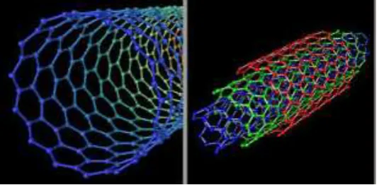
Carbon Nano Tube (CNT) has been considered as one of the most important building blocks in nano devices. Carbon Nano Tubes were discovered by S. Ijiima in 1991 while performing some experiments on molecular structure composed of carbonium [1]. CNTs are hollow cylinder composed of one or more concentric layers of carbon atoms in a honey comb lattice arrangement. It can be classified into Single Walled Carbon Nano Tube (SWCNT) and Multi Walled Carbon Nano Tube (MWCNT).
IJEDR1604100
International Journal of Engineering Development and Research (www.ijedr.org)664
The way graphite sheet is rolled represented by a pair of indices (n, m) called chiral vector. CNT with n-m = 3 are metals, otherwise they are semiconductors. One of the best applicable properties of CNT is ballistic transportation of electrons along the tube; therefore semiconducting CNT can be used as channel for transistors [2].Figure 2: Metallic and Semiconducting CNT
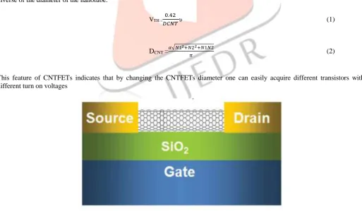
CNTFETs working are same like conventional silicon transistors. CNTFETS are of different types and one of them is Schottky Barrier CNTFET (SB-CNTFET). These transistors are constructed with a semiconducting nanotube and two metallic contacts acting as source and drain; hence they have Schottky Barrier at the metal nanotube junction. In this type of CNTFETS, by changing the barrier height at the metal semiconductor interface, gate modulates the injection of carriers in the nanotube. Due to exhibit strong ambipolar characteristics, SB-CNTFETS are suitable for using in CMOS logic families. Another type of CNTFET is MOSFET like CNTFET (MOS-CNTFET) which exhibit unipolar behavior unlike SB-CNTFET. In this MOSFET like device, the ungated portion (source and drain regions) is heavily doped and the CNTFET operates on the principle barrier height modulation by application of the gate potential. The conductivity of MOS CNTFETs is modulated by the gate –source bias. Both SB-CNTFETs and MOS-CNTFETs areused for high speed design because of their ON current, band to band tunneling CNTFET (T-CNTFET) is utilized for ultra Low power design on account of its low ON current and super cut-off attributes [3-5]. CNTFETs has a useful property that it will ease circuit designing and increase circuits performance on the other hand, which is that proportional to the inverse of the diameter of the nanotube.
VTH = 0.42
𝐷𝐶𝑁𝑇 υ (1)
DCNT =
𝛼√𝑁12+𝑁22+𝑁1𝑁2
𝜋 (2)
This feature of CNTFETs indicates that by changing the CNTFETs diameter one can easily acquire different transistors with different turn on voltages
Figure 3 : Structure of CNTFET
CNTFET technology provides more efficient way to implement these functions in terms of Delay, Power consumption and Area. As shown in equation 1, voltage threshold is proportional to the 1/DCNT and it could be justified by manipulating N1 and N2, which
IJEDR1604100
International Journal of Engineering Development and Research (www.ijedr.org)665
III.PROPOSED DESIGNS AND SIMULATION RESULTS OF LOGIC GATES
Basic functions such as AND, OR and buffer can be implemented by generating related inverting fuction (e.g. NAND, NOR and NOT) followed by an inverter [5-8].
1. NOT Gate
Figure 4 shows an inverter comprising of P-type and N-type CNTFETs. They are coupled together in series between a high supply voltage VDD and a low supply VSS as shown.
Figure 4: Structure of CNTFET NOT Gate and its behavior
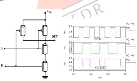
2. NAND Gate
Figure 5 shows NAND gate comprising of CNTFETs. It comprises of driver CNTFETs coupled together in parallel between a high supply reference VDD and a series active load transistors, which is coupled to a low supply reference VSS as
shown.
IJEDR1604100
International Journal of Engineering Development and Research (www.ijedr.org)666
3. NOR Gate
Figure6 shows NOR gate comprising of CNTFETs. It comprises of driver CNTFETs coupled together in series between a high supply reference VDD and a parallel connected active load transistors, which is coupled to alow supply reference VSS as
shown.
Figure 6: Structure of CNTFET NOR Gate and its behavior
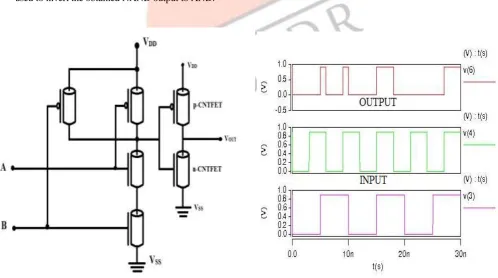
4. AND Gate
Figure 7 shows AND gate comprising of CNTFETs. It consists of driver p-CNTFET coupled together in parallel between a high supply reference VDD and a series active load transistors, which is coupled to ground terminal as shown. An Inverter is
used to invert the obtained NAND output to AND.
IJEDR1604100
International Journal of Engineering Development and Research (www.ijedr.org)667
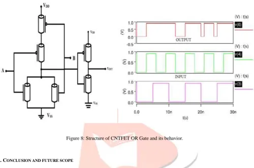
5. OR Gate
Figure 8 shows OR gate comprising of p-type and n-type CNTFETs. The p-type CNTFETs are placed in series between high supply reference VDD and n-type CNTFETs are placed in parallel, which is coupled to ground terminal, as shown. An
inverter is used to invert the obtained NOR output to OR gate.
Figure 8: Structure of CNTFET OR Gate and its behavior.
IV.CONCLUSION AND FUTURE SCOPE
This paper adequately explains the various modeling aspects of the proposed CNTFET. The various circuits such as NOT, NAND, NOR gates designed using CNTFETs. Basic functions such as AND,OR in CMOS technology are implemented by generating functions (e.g. NAND, NOR) followed by an inverter. Voltage threshold losing which occurred in passing high and low voltages in n-MOSFET and p-MOSFET, respectively results in such implementation. CNTFET technology provides more efficient way to implement these functions in terms of delay, power consumption and area. Voltage threshold is proportional to the 1/DCNT, so
increasing the diagonal of nanotube (i.e. DCNT) results in decreasing the voltage threshold toward zero. With the help of these basic
gates we can design various combinational circuits such as adder, subtractor, mux, decoder etc. as well as various sequential circuits. They can be even utilized in designing ternary logic circuits.
REFERENCES
[1] S.Iijima, “Helical Microtubes of graphitic carbon”, Nature, Vol. 354, no.6348, Nov. 1991, pp.56-8.
[2] NeetuSardana, L.K.Ragha, “Carbon Nano Tube Field Effect Transistor: A Review” International Journal of Engineering Sciences and Research Technology.Vol. 5, No.3, April, 2016
[3] R. Martel, T. Schmidt, HR Shea, T.Hertel, and Ph. Avouris,(1998), “Single and multi-wall carbon nano tube field-effect transistors” Appl. Phys. Lett. 73, 2447
[4] J. Deng, (227) “Device modeling and circuit performance evaluation for nanoscales devices: silicon technology beyond 45 nm and carbon nanotube field effect transistors, “Doctoral Dissertation, Stanford University
[5] FazelSharifi, “CNTFET Based Gates and a Novel Full Adder Cell”, International Journal of VLSI design & communication Systems (VLSICS) Vol.3, No.3, June 2012.
[6] S.V.Srikanth, “Design of logic gates using CNTFETs”, ISSN:2394-3661, Vol. 2, Issue-4, April 2015. [7] Yasuyunki Miura, “An Universal Logic-circuit with Flip-Flop based on DG-CNTFET”, IEEE 2013.