„
2
ⴛ
4
…
GaP
„
001
…
surface: Atomic structure and optical anisotropy
A. M. Frisch
Institut fu¨r Festko¨rperphysik, Technische Universita¨t, Hardenbergstraße 36, 10623 Berlin, Germany
W. G. Schmidt and J. Bernholc
Department of Physics, North Carolina State University, Raleigh, North Carolina 27695-8202
M. Pristovsek, N. Esser, and W. Richter
Institut fu¨r Festko¨rperphysik, Technische Universita¨t, Hardenbergstraße 36, 10623 Berlin, Germany 共Received 17 December 1998兲
We have investigated the microscopic structure and optical anisotropy of (2⫻4) reconstructed GaP共001兲 surfaces. Optical and electron spectroscopy from GaP共001兲surfaces prepared in ultrahigh-vacuum conditions were combined with first-principles calculations of the energetics and reflectance anisotropy. Symmetry, com-position and surface optical anisotropy were characterized by low-energy electron diffraction, Auger electron spectroscopy, photoemission spectroscopy and reflectance anisotropy spectroscopy. In contrast to most earlier reports, we find that the stable Ga-rich surface corresponds to a (2⫻4) reconstruction. No (4⫻2) reconstruc-tion could be observed, independent of the preparareconstruc-tion method. Depending on the Ga coverage, however, two distinct line shapes in the reflection anisotropy spectra occur, indicating the existence of at least two different surface phases with (2⫻4) periodicity. This agrees with our total-energy calculations: Four (2⫻4) structural models may be stable depending on the chemical potentials of the surface constituents. All considered (4
⫻2) structures, however, are unstable. Based on the comparison between calculated reflectance anisotropy spectra and measured data we suggest mixed Ga-P dimers on top of the Ga-terminated substrate as ground-state geometry for the cation-rich phase of GaP共001兲(2⫻4). Our results indicate the formation of P dimers at the surface for the more anion-rich phase of GaP共001兲(2⫻4).关S0163-1829共99兲02828-3兴
I. INTRODUCTION
Much progress has been made in recent years in under-standing the microscopic structure of the growth planes of III-V compound semiconductors 共for a recent review see, e.g., Ref. 1兲. This does not hold, however, for GaP. The experimental studies carried out so far arrive at different and partially contradicting conclusions about the symmetry and structure of the GaP共001兲 surface. In most publications, it has been suggested that ion bombardment and annealing of GaP共001兲results in a (4⫻2)/c(8⫻2) reconstructed, Ga-rich surface,2–7 in analogy to the corresponding Ga-rich GaAs共001兲surface structure.8A (4⫻2)/c(8⫻2) reconstruc-tion was also reported for Ga-rich GaP共001兲 prepared by decapping of P- and As-protective layers.9 In that experi-ment, however, a residual As contamination was present on the surface. In gas source molecular-beam epitaxy 共MBE兲 experiments10 it was found that (2⫻4) and (4⫻2) recon-struction patterns correspond to P- and Ga-stabilized sur-faces. In Ref. 4, on the other hand, clear differences between the scanning tunneling microscopy 共STM兲 images recorded on sputtered/annealed GaP共001兲surfaces and the correspond-ing data for GaAs共001兲(4⫻2)/c(8⫻2) surfaces11 are re-ported. In a more recent publication by the same group,12 examining the atomic structure by ion scattering, the symme-try was corrected to a (2⫻4). (2⫻4) reconstructions under Ga as well as under P supply were also observed in MBE experiments of Ref. 13. Additionally, the authors found an intermediate (4⫻4) reconstruction during layer growth and suggested the formation of Ga droplets on a (2⫻4)
recon-structed surface for high amounts of Ga supply. In a recent atomic layer MBE work,14 (2⫻2)- and (2⫻ 4)-recon-structions were observed by reflection high-energy electron diffraction for P- and Ga-rich surfaces, respectively.
Apart from the ambiguous findings for the symmetry of the stable GaP共001兲 surface, a wide variety of geometrical models were discussed for its surface structure: in analogy to GaAs共001兲, (4⫻2), and 2(4⫻2) structures were sug-gested based on electron spectroscopy9 and STM 共Ref. 3兲 experiments, respectively. Basically the same structure, but with a much larger dimer separation, was put forward in Ref. 5. On base of time-of-flight scattering and recoiling spectros-copy a (2⫻4) Ga-trimer structure6was proposed, in analogy to according previous work on InP共001兲.15 On the basis of ion scattering experiments a Ga double-layer structure12and, finally, in a very recent STM study a Ga single-dimer struc-ture was suggested.16
Besides the puzzling experimental results there exists, to our knowledge, only one theoretical study17so far, based on a semiempirical method. In that work, several (2⫻4) dimer geometries are suggested. The energetic comparison, how-ever, is complicated, since only desorption energies are given.
While the atomic surface structure of GaP共001兲 is still controversial, recent studies of In-rich InP共001兲surfaces are available:15,18–21Experiments and calculations reveal that the microscopic structure of the cation-rich InP共001兲surface dif-fers from the well-investigated GaAs共001兲surface8,22,23 due to the large size difference between cations and anions. The size ratio between the covalent radii of cations and anions is
PRB 60
about 1.36 for InP compared to 1.19 for GaP and 1.05 for GaAs.24 Based on the simple concept of covalent radii, GaP共001兲surface structures can therefore be expected also to deviate from the ones observed for GaAs.
In the present paper, clean, reconstructed GaP共001兲 sur-faces are characterized in ultra high vacuum共UHV兲by low-energy electron diffraction共LEED兲, Auger electron spectros-copy共AES兲and reflectance anisotropy spectroscopy共RAS兲. A variety of plausible structural models for (2⫻4) and (4 ⫻2) reconstructed surfaces are probed by ab initio total-energy calculations. For the energetically favored structures we compute the RAS spectra. The comparison of the experi-mental data with the calculated surface-phase diagram and optical spectra indicates the existence of at least two distinct (2⫻4) reconstructions.
II. EXPERIMENTAL
A. Surface preparation
The GaP共001兲surfaces were prepared by thermal desorp-tion of a protective arsenic/phosphorus double layer 共cap兲 under UHV conditions. For this purpose homoepitaxial GaP epilayers were grown by metal organic vapor phase epitaxy 共MOVPE兲 on highly n-doped GaP共001兲 substrates and capped in situ utilizing the photodecomposition of phosphine and arsine by an eximer laser source.20,25 The thermal de-sorption of the protective arsenic/phosphorus layer was per-formed in UHV共base pressure⭐10⫺10hPa兲by annealing to 690 K using an indirect resistive heating. Surface stoichiom-etry was modified by successive annealing steps up to 1000 K共the sample was kept at constant final temperature for five minutes in each annealing step兲. For comparison, surfaces were also prepared by sputtering and annealing, following the same experimental conditions as reported in literature2–7 共400-eV Ar⫹ ions, annealing temperature 725 K兲. The GaP共001兲 surfaces were cooled down to room temperature and investigated by LEED, RAS, and AES.
B. Results
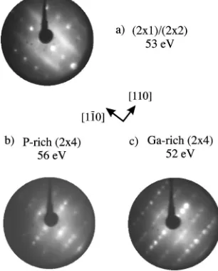
The decapped GaP共001兲 surfaces共after annealing to 690 K兲show a (2⫻1)/(2⫻2)-like LEED pattern关see Fig. 1共a兲兴, with clear (2⫻1)-spots plus additional weak streaks in the 关110兴half-order position. Corresponding diffraction patterns under P-rich conditions are also observed on InP共001兲 surfaces26,27 which, according to a recent STM study,26 are terminated by P-surface dimers arranged in different local structures. Annealing to 785 K leads to a (2⫻4) LEED pat-tern. Due to not fully resolved fractional order spots in the 关110兴 direction, the LEED pattern of this surface does not allow us to distinguish clearly between a (2⫻4) and a (2⫻4)/c(2⫻8) reconstruction关Fig. 1共b兲兴. Upon further an-nealing up to 1000 K the quality of the LEED pattern is improved. The former streaks develop into sharp spots indi-cating a pure (2⫻4) reconstruction关Fig. 1共c兲兴. Upon anneal-ing to still higher temperatures the symmetry remains un-changed until the surface deteriorates by forming Ga droplets, as indicated by a metallic component in the Ga 3d core-level photoemission line 共not shown here兲. The P/Ga ratio determined by AES at the (2⫻4) reconstructed surface for low-annealing temperatures 共only slightly above 785 K兲
is very close to the one found on the stoichiometric balanced 共110兲 cleavage surface of GaP. Upon annealing to higher temperatures 共1000 K兲 the ratio changes successively by a factor of approximately two towards a Ga-rich surface, sug-gesting the existence of distinct (2⫻4)-reconstructions, be-ing more P-rich at lower and more Ga-rich at higher anneal-ing temperatures.
Real parts of different RAS spectra recorded from GaP共001兲 surfaces are shown in Fig. 2共a兲. For the sake of comparison, RAS spectra of the (2⫻1)/(2⫻2)-like and (2⫻4) InP共001兲and the2(2⫻4) GaAs共001兲are shown in Fig. 2共b兲. Three different spectral line shapes are reproduc-ibly observed on GaP共001兲, correlated with the surface preparation: characteristic spectra belonging to the (2⫻1)/(2⫻2)-like structure, the P-rich (2⫻4) structure at lower annealing temperature and the Ga-rich (2⫻4) struc-ture at higher annealing temperastruc-ture. The P-rich GaP共001兲 (2⫻4) surface 共middle curve兲 shows a spectrum, which is qualitatively similar to the one observed for the As-dimer terminated2(2⫻4) GaAs共001兲surface.28,29It is character-ized by pronounced maxima at 3.5 and 4.8 eV, close to the
E1 and E0
⬘
gap energies of GaP 共3.69 and 4.77 eV, respectively30兲and a weak maximum between the gaps, at 4 eV. After annealing to higher temperatures the spectrum changes into a line shape similar to the one observed for the mixed In-P dimer terminated InP共001兲(2⫻4) surface.31–34 New features in this spectrum are a strong minimum at 2.4 eV and a maximum at 3.2 eV, significantly below the E1gap of GaP. The maxima around 4 eV and at 4.8 eV found on the P-rich (2⫻4) surface are still present.A (2⫻4) LEED pattern is also observed from共001兲 sur-faces prepared by sputtering and annealing. The P/Ga AES ratio on this surface is close to the one found at intermediate annealing temperatures 共875 K兲 on the decapped surfaces. The RAS spectrum, however, corresponds to that of the Ga-rich structure of the decapped GaP共001兲surfaces.
Summarizing the RAS results, there are clear similarities between GaP共001兲 and InP共001兲 for the very anion-rich
FIG. 1. LEED patterns recorded from GaP共001兲: 共a兲 (2
(2⫻1)/(2⫻2)-like and the very cation-rich (2⫻4) recon-structed surfaces, in particular if one accounts for the differ-ent bulk critical-point energies of the two materials. The spectrum of the P-rich (2⫻4) reconstructed GaP共001兲 sur-face, however, resembles the one of GaAs共001兲2(2⫻4). The evolution of the RAS spectra with increasing Ga surface coverage implies that at least two distinct (2⫻4) structures with different stoichiometry exist on GaP共001兲. To address this question, we have performed ab initio calculations of the energetics and surface optical properties, which are presented below.
III. THEORY AND DISCUSSION
A. Computational
The calculations were based on density-functional theory in local-density approximation 共DFT-LDA兲. The electron-ion interactelectron-ion was described by nonlocal norm-conserving pseudopotentials.35 The Ga 3d electrons are partially taken into account by means of a nonlocal core correction to the exchange and correlation energy. The electronic degrees of freedom were relaxed using a recently developed real-space multigrid technique.36,37This approach provides for effective convergence acceleration and preconditioning on all length scales. Furthermore, it allows for an efficient parallelization and is thus particularly suitable for large surface reconstruc-tions as studied here. The spacing of the finest grid used to represent the electronic wave functions and charge density was determined through a series of GaP bulk calculations. We find structural and electronic properties to be converged for a spacing of 0.238 Å . This corresponds to an energy cutoff in plane-wave calculations of about 24 Ryd. Through-out the calculations we use the calculated equilibrium lattice constant of 5.39 Å , which is slightly smaller than the mea-sured value 关5.45 Å共Ref. 38兲兴. More severe is the underes-timation of the electronic excitation energies due to the DFT-LDA band-gap problem. We determine the values of 1.46,
1.68, 2.09, and 3.97 eV for E(X1c), E(X3c), E(⌫1c), and E(⌫15c). These energies are about 0.7 – 0.9 eV smaller than measured. The same almost constant shift is observed for the
E0, E1, and E0
⬘
critical points of the bulk electronic struc-ture, for which we calculate values of 2.1, 2.9, and 4.0 eV. To model the GaP共001兲surface we consider a periodic super cell along the surface normal. It contains 8/12 atomic共001兲 layers and a vacuum region equivalent in thickness to 8 atomic layers for calculations of the energetic/optical prop-erties. The dangling bonds at the bottom layer of the slab are saturated with pseudohydrogens. The geometries of the in-vestigated models were relaxed until all calculated forces were below 25 meV/Å . Integrations in the surface Brillouin zone共SBZ兲for calculating the atomic and electronic ground state of the surface were performed using four special k points in the irreducible part. For the calculation of the di-electric function we included all conduction bands within 8 eV of the top of the valence bands, using 16 uniformly dis-tributed k points in the irreducible part of the SBZ. This corresponds to 256 k points in the full (1⫻1) SBZ.B. Surface phase diagram
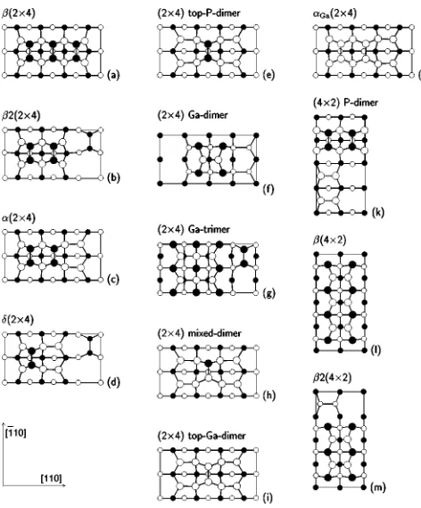
One essential ingredient for calculations of surface ground-state structures is the choice of appropriate starting geometries for optimization. This holds in particular for large surface reconstructions as studied here. Figure 3 gives a top view of the relaxed geometries of all structures considered in this work.
共001兲surfaces of III-V compounds are usually explained in terms of the surface structures known from GaAs.39 Therefore, the,2,␣ and anion-dimer models关Figs. 3共a兲, 3共b兲, 3共c兲, 3共j兲, 3共l兲, and 3共m兲兴 suggested for GaAs 共Refs. 1,8,22,23, and 40兲 were considered. On the other hand, as outlined in the introduction, the size difference between cat-ions and ancat-ions may lead to GaP surface structures different from GaAs. In case of InP it was noted that the formation of FIG. 2. Real parts of 关(r[1⫺10]-r[110])/具r典兴*10
3
s p2-hybridized cation dimers at the surface causes appre-ciable stress in the subsurface layers due to the large size difference between the substrate constituents.23At this point, we want to emphasise further similarities between GaP and InP共001兲 surfaces: 共i兲 The reconstructions evolve similarly from a (2⫻1)/(2⫻2)-like phase for anion-rich to (2⫻4) for more cation-rich surfaces, 共ii兲 as discussed above, GaP and InP show similar features in their anisotropic optical response, and共iii兲the surface core-level shifts measured for cation-rich InP and GaP surfaces are qualitatively very similar.16,19Thus, it appears plausible to include in our study also the single-dimer structures shown in Figs. 3共e兲, 3共h兲, and 3共i兲, which were assumed to exist on InP共001兲19. These cation-rich structures allow to saturate all surface bonds and avoid or at least reduce the stress caused by the formation of cation-cation dimers. For the same reason also the ␦ struc-ture关Fig. 3共d兲兴, which is believed to describe the Sb-induced GaAs(2⫻4) reconstruction,41may be a plausible candidate. Besides the models mentioned above we include in our cal-culations also the structures Figs. 3共f兲, 3共g兲, 3共j兲, 3共k兲, and 3共l兲which have been suggested for GaP共001兲based on pre-vious experimental work3,5,6,9,12 共see Introduction兲. We would like to note that the model Fig. 3共f兲corresponds to the structure of lowest energy we derive from the class of struc-tures proposed in a recent STM study.16 In our previous work on InP共001兲an according structure was already tested and found to be energetically unfavourable.19
The investigated models realize different Ga coverages: ⌰⫽1/4关(2⫻4) and 2(2⫻4)], ⌰⫽1/2(␣ and ␦), ⌰ ⫽3/4 关top-P-dimer, Ga-trimer, (2⫻4) Ga dimer, (4⫻2)
and 2(4⫻2)], ⌰⫽1 共mixed-dimer兲, ⌰⫽5/4 for 共top-Ga dimer兲and⌰⫽6/4关␣Ga(2⫻4)兴.42An energetic comparison of these structures can therefore only be made by taking into account the chemical potentials of the surface constituents.23 In Fig. 4, we show the relative formation energies of the considered surface structures vs the Ga chemical potential. For rich surfaces mixed P dimers on top of an Ga-terminated surface关Fig. 3共h兲兴are favoured. For less Ga-rich conditions P-dimers in a 2(2⫻4) geometry 关Fig. 3共b兲兴, known from As-rich GaAs共001兲surfaces,22,43are stable. For intermediate values of the Ga chemical potential the
␦(2⫻4) phase关Fig. 3共d兲兴may occur. In the extreme Ga-rich limit the top-Ga-dimer model 关Fig. 3共i兲兴 is stable. Before comparing the calculated phase diagram with the experi-ments, we want to underline that only (2⫻4) and (4⫻2) reconstructions are addressed here. Other surface symme-tries, which may be favored for very P-rich conditions, were not considered. The phase diagram in Fig. 4 agrees well with our experimental findings: 共i兲 The stable, Ga-rich GaP共001兲 surface reconstructs in (2⫻4) symmetry. Among the (4⫻2) reconstructions the energetically most favored one, the GaP共001兲2(4⫻2) structure, is about 0.1 eV per surface atom higher in energy than the (2⫻4) top-P-dimer model. Therefore, it is very unlikely to be an equilibrium structure. 共ii兲Different (2⫻4) surface phases occur depending on the actual value of the Ga chemical potential, i.e., the surface preparation conditions.共iii兲The phase diagram is very simi-lar to that of InP共001兲,19as suggested by the evolution of the optical spectra discussed above. The similarity between the surface phase diagrams of InP and GaP is likely to be caused by the same mechanism: The size difference between anions and cations which favors the formation of single-dimer struc-tures for cation-rich surfaces over the accomodation of
s p2-hybridized cation dimers that are typical for GaAs共001兲 surfaces. The ␦, mixed-dimer and top-Ga-dimer models are characterized by strong Ga-Ga bonds 共bond lengths 2.47 – 2.62 Å兲 in the second atomic layer. The dimer lengths are 2.44 Å for the Ga-Ga dimer of the top-Ga-dimer model, 2.23–2.25 Å for the P-P dimers of the 2 and␦ structure, and 2.36 Å for the Ga-P dimer for the mixed-dimer model. FIG. 3. Top view of relaxed GaP共001兲(2⫻4) and (4⫻2)
sur-face reconstruction models. Empty共filled兲circles represent Ga共P兲 atoms. Large 共small兲 symbols indicate positions in the first and second共third and fourth兲atomic layers. (2⫻4) and (4⫻2) recon-structions are ordered by increasing Ga coverage.
FIG. 4. Relative formation energy共with respect to the P-trimer structure兲per (1⫻1) unit cell for GaP共001兲surface reconstructions vs⌬(Ga)ªbulk(Ga)⫺(Ga). The approximate
thermodynami-cally allowed range: ⫺⌬Hf(GaP)关⫽0.91 eV 共Ref. 51兴
These values are in good agreement with the sum of the respective covalent radii24 and the corresponding bond lengths at GaAs共001兲 共Refs. 22,23, and 43兲 and InP共001兲 surfaces.21 All equilibrium structures are in agreement with electron counting heuristics.44
C. Optical anisotropy
While the calculated phase diagram is in agreement with our experimental data, a more direct comparison between theory and measurement is desirable in order to identify spe-cific surface structures. To this end we compute the reflec-tance anisotropy of the energetically favoured structures. The calculations are carried out in independent-particle approxi-mation based on the electronic structure obtained within DFT-LDA. We follow the formalism developed by Del Sole45and Manghi et al.46 Our calculations are on the same footing as a recent study of the optical properties of InP共001兲 surfaces,34 where further details can be found.
The calculated spectra are shown in Fig. 5共a兲. The top-Ga-dimer, mixed-dimer, and␦ structures show a pronounced negative anisotropy in the low-energy region, with minima between 2.0 and 2.3 eV. The strength of that anisotropy is directly correlated to the number of Ga-Ga bonds along the 关110兴direction. Its magnitude is highest for the top-Ga-dimer model with eight bonds, slightly reduced and shifted to lower energies for the mixed-dimer geometry with six cation-cation bonds and flattened for the ␦ structure with only two such bonds. The calculated spectra also show a strong dependence
on structural details for higher energies. For the2 geometry with three P-P dimers oriented along 关11¯ 0兴 we find a rela-tively broad positive anisotropy between about 2.4 and 4.4 eV. Maxima of the anisotropy appear around 3.2 and 4.1 eV and a shoulder exists at 2.8 eV. The shape of that anisotropy is roughly preserved for the␦ structure, which features one P-P dimer. The magnitude of the anisotropy, however, is somewhat reduced and the spectrum is shifted downwards. An even further reduction in positive anisotropy occurs for the mixed-dimer and top-Ga-dimer structures, featuring single P or Ga dimers, respectively, on top of a Ga-terminated substrate. The described evolution of the spectra in the high-energy region shows thus a correlation between the positive anisotropy and the formation of P-P dimers.
In order to better understand the origin of the surface anisotropy we performed further calculations. Figure 5共b兲 shows the calculated RAS for the four surface geometries taking into account only transitions within the uppermost four atomic layers. These are the layers where most of the surface related structural and electronic modifications occur. The calculated spectra are rather similar to those calculated for the complete slab. In particular, this holds for the nega-tive anisotropy around 2 eV, which can therefore be attrib-uted to near-surface transitions. A similar feature at InP共001兲 was explained by transitions between cation-cation bonding states and empty dangling bonds at threefold coordinated surface cations.34The anisotropies at higher energies are less well reproduced by near-surface transitions. We find a rela-tively broad positive anisotropy above 3.3 eV for the2 and
␦ structures, which is absent for mixed-dimer and top-Ga-dimer structure. In a recent study of InP共001兲 共Ref. 34兲this anisotropy was traced back to transitions between occupied anion-dimer states and unoccupied surface resonances. Also shown in Fig. 5共b兲are the contributions to the optical anisot-ropy due to transitions below the uppermost four layers 共dashed lines兲. For all investigated structures these transi-tions between predominantly bulklike states give rise to fea-tures at the bulk critical points that depend only weakly on the surface structure and stoichiometry. In particular, all curves show minima around 3.6 eV and maxima at about 4.1 eV, close to the calculated E0
⬘
gap. This reflects the general trend that surface transitions often dominate the low-energy part and bulklike transitions are more pronounced in the high-energy part of the RAS spectra.The comparison with the experimental spectra is compli-cated by the DFT-LDA band-gap problem. As discussed above, a redshift of about 0.7 – 0.9 eV for the bulk-related features arises from the underestimation of the bulk excita-tion energies. This shift does not necessarily apply to the transitions between surface states. Quasiparticle calculations for semiconductor surfaces including many-body effects in GW approximation47–49have shown that bulk- and surface-state energies may experience different shifts with respect to the eigenvalues of the underlying DFT-LDA calculation. In particular, Hybertsen and Louie47 point out that, depending on the orbital character of the specific states, the surface band gap may actually open much less than the bulk gap, when self-energy effects are included in the calculations. Electron-hole interaction effects50 can also be expected to change the position and magnitude of anisotropy features. Unfortunately, both self-energy and electron-hole interaction FIG. 5. 共a兲: RAS spectra兵Re关(r[1⫺10]⫺r[110])/具r典兴其 calculated
for the energetically favored structural models of the GaP共001兲(2
effects are beyond the scope of our work. If these limitations are borne in mind, however, a meaningful comparison be-tween experimental and calculated spectra can still be made. The RAS spectrum measured for the (2⫻4) structure pre-pared at higher annealing temperature 共Ga-rich phase兲 fea-tures a strong negative peak in the low-energy region. Given the energy position of this peak and its dependence on the preparation conditions, it is very likely that it is surface re-lated and can be identified with the calcure-lated negative an-isotropy arising from Ga-Ga bonding related states described above. Both the top-Ga-dimer model and the mixed-dimer model thus appear plausible candidates to explain the Ga-rich surface phase. The measured spectrum for the Ga-Ga-rich phase shows further maxima between the energies of the E0 and E1 critical points and at the E0
⬘
bulk peak. The latter maximum at the corresponding energy of about 4 eV is present in the calculated spectra of all considered structures. The first peak, which should be observed between 2.1 and 2.9 eV in the calculated spectrum, is completely absent in case of the top-Ga-dimer structure; it appears, however, as a weak shoulder for the mixed-dimer model. Therefore we identify the Ga-rich phase of the GaP共001兲(2⫻4) surface tentatively with the mixed-dimer model. This assignment is corroborated by very recent surface core-level shift measure-ments on Ga-rich GaP共001兲(2⫻4) surfaces,16 where one P2 p and two Ga3d surface components were found. The Ga-surface components were assigned to threefold coordi-nated Ga atoms and Ga-Ga bonds. These two components can be explained both by the top-Ga-dimer structure and the mixed-dimer model. Only the latter, however, provides an explanation for the finding of a surface P component, sup-posed to arise from threefold coordinated P atoms.The measured spectrum for the (2⫻4) structure annealed at lower temperature 共less Ga-rich phase兲is dominated by a
‘‘camelback’’ overall spectrum shape with maxima between the energies of the E0 and E1 critical points and at the E0
⬘
bulk peak. No negative anisotropy appears. The only com-puted spectrum with no 共or very little兲 negative anisotropy belongs to the 2(2⫻4) structure. Maxima appear at 3.2 and 4.1 eV, close to the calculated energies of the E1and E0⬘
critical points. Our results thus indicate that the P-rich phase of the GaP共001兲(2⫻4) surface corresponds to the 2(2 ⫻4) structure in analogy to As-rich GaAs共001兲surfaces.IV. CONCLUSIONS
In conclusion, we have presented a comprehensive study of the atomic structure of (2⫻4) reconstructed GaP共001兲 surfaces based on electron spectroscopy, the investigation of the optical anisotropy and the energetics of the surface. Both for a balanced surface stoichiometry and for Ga-rich condi-tions, we find (2⫻4) reconstructed surfaces that are stabi-lized by the formation of dimers. Experiment as well as theory suggest the existence of at least two different (2 ⫻4) surface phases, depending on the Ga content of the surface. Our results indicate that mixed Ga-P dimers on top of an terminated surface are the ground state of the Ga-rich phase, analogously to InP共001兲(2⫻4). For the less Ga-rich surface phase we suggest the formation of P-P dimers in a2(2⫻4) geometry, as observed for GaAs.
ACKNOWLEDGMENTS
Financial support by BMBF-Verbundprojekt 22, DFG共Es 127/4-1, Schm 1361/1-1兲, NSF 共Grant No. DMR 9408437兲 and ONR 共Grant No. N00014-96-I-0161兲 is gratefully ac-knowledged. This work was supported in part by grants of supercomputer time from the DoD Challenge Program and the North Carolina Supercomputer Center.
1Q.-K. Xue, T. Hashizume, and T. Sakurai, Prog. Surf. Sci. 56, 1 共1997兲, and references therein.
2Y. Fukuda, M. Shimomura, N. Sanada, and N. Nagoshi, J. Appl.
Phys. 76, 3632共1994兲.
3N. Sanada, M. Shimomura, Y. Fukuda, and T. Sato, Appl. Phys.
Lett. 67, 1432共1995兲.
4A. Watanabe, H. Shimaya, M. Naitoh, and S. Nishigaki, J. Vac.
Sci. Technol. B 14, 3599共1996兲.
5M. Naitoh, A. Watanabe, A. Konishi, and S. Nishigaki, Jpn. J.
Appl. Phys., Part 1 35, 4789共1996兲.
6M.M. Sung and J.W. Rabalais, Surf. Sci. 365, 136共1996兲. 7N. Oishi, F. Shoji, A. Konishi, M. Naitoh, and S. Nishigaki, Surf.
Rev. Lett. 5, 223共1998兲.
8D.K. Biegelsen, R.D. Bringans, J.E. Northrup, and L.-E. Swartz,
Phys. Rev. B 41, 5701共1990兲.
9I.M. Vitomirov, A. Raisanen, L.J. Brillson, C.L. Lin, D.T.
McIn-turff, P.D. Kirchner, and J.M. Woodall, J. Vac. Sci. Technol. A 11, 841共1993兲.
10J.N. Baillargeon, K.Y. Cheng, and K.C. Hsieh, Appl. Phys. Lett.
56, 2201共1990兲.
11Q.-K. Xue, T. Hashizume, J.M. Zhou, T. Sakata, T. Ohno, and T.
Sakurai, Phys. Rev. Lett. 74, 3177共1995兲.
12M. Naitoh, A. Konishi, H. Inenaga, S. Nishigaki, N. Oishi, and F.
Shoji, Surf. Sci. 402-404, 623共1998兲.
13M. Yoshikawa, A. Nakamura, T. Nomura, and K. Ishikawa, Jpn.
J. Appl. Phys., Part 1 , 35, 1205共1995兲.
14
P.A. Postigo, G. Armelles, and F. Briones, Phys. Rev. B 58, 9659
共1998兲.
15M.M. Sung, C. Kim, H. Bu, D.S. Karpuzov, and J.W. Rabalais,
Surf. Sci. 322, 116共1995兲.
16N. Sanada, S. Mochizuki, S. Ichikawa, N. Utsumi, M.
Shimo-mura, G. Kaneda, A. Takeuchi, Y. Suzuki, Y. Fukuda, S. Tanaka, and M. Kamata, Surf. Sci. 419, 120共1999兲.
17E.V. Stefanovich and A.L. Shluger, J. Phys.: Condens. Matter 6,
4255共1994兲.
18C.D. MacPherson, R.A. Wolkow, C.E.J. Mitchell, and A.B.
McLean, Phys. Rev. Lett. 77, 691共1996兲.
19W.G. Schmidt, F. Bechstedt, N. Esser, M. Pristovsek, Ch.
Schultz, and W. Richter, Phys. Rev. B 57, 14 596共1998兲.
20N. Esser, U. Resch-Esser, M. Pristovsek, and W. Richter, Phys.
Rev. B 53, R13 257共1996兲.
21W.G. Schmidt and F. Bechstedt, Surf. Sci. 409, 474共1998兲. 22J.E. Northrup and S. Froyen, Mater. Sci. Eng., B 30, 81共1995兲. 23W.G. Schmidt, Appl. Phys. A: Mater. Sci. Process. 65, 581
共1997兲.
Sci-entific Company, Skokie, IL, 1980兲.
25K. Knorr, M. Pristovsek, U. Resch-Esser, N. Esser, M. Zorn, and
W. Richter, J. Cryst. Growth 170, 230共1997兲.
26
P. Vogt, Th. Hannappel, S. Visbek, K. Knorr, N. Esser, and W. Richter, Phys. Rev. B共to be published兲.
27N. Esser, W.G. Schmidt, J. Bernholc, A.M. Frisch, P. Vogt, M.
Zorn, M. Pristovsek, W. Richter, F. Bechstedt, Th. Hannappel, and S. Visbeck, J. Vac. Sci. Technol. B共to be published兲.
28I. Kamiya, D.E. Aspnes, L.T. Florez, and J.P. Harbison, Phys.
Rev. B 46, 15 894共1992兲.
29A.I. Shkrebtii, N. Esser, W. Richter, W.G. Schmidt, F. Bechstedt,
B.O. Fimland, A. Kley, and R. Del Sole, Phys. Rev. Lett. 81, 721共1998兲.
30S. Zollner, M. Garriga, J. Kirchner, J. Humliicek, and M.
Car-dona, Phys. Rev. B 48, 7915共1993兲.
31K.B. Ozanyan, P.J. Parbrook, M. Hopkinson, C.R. Whitehouse,
Z. Sobiesierski, and D.I. Westwood, J. Appl. Phys. 82, 474
共1997兲.
32 M. Zorn, T. Trepk, J.-T. Zettler, B. Junno, C. Meyne, K. Knorr,
T. Wethkamp, M. Klein, M. Miller, W. Richter, and L. Samuel-son, Appl. Phys. A: Mater. Sci. Process. 65, 333共1997兲.
33J. Kinsky, Ch. Schultz, D. Pahlke, A.M. Frisch, T. Herrmann, N.
Esser, and W. Richter, Appl. Surf. Sci. 123, 228共1998兲.
34W.G. Schmidt, E.L. Briggs, J. Bernholc, and F. Bechstedt, Phys.
Rev. B 59, 2234共1999兲.
35D.R. Hamann, Phys. Rev. B 40, 2980共1989兲; L. Kleinman and
D.M. Bylander, Phys. Rev. Lett. 48, 1425共1982兲; M. Fuchs and M. Scheffler, Comput. Phys. Commun. 119, 67共1999兲.
36E.L. Briggs, D.J. Sullivan, and J. Bernholc, Phys. Rev. B 52,
R5471共1995兲.
37E.L. Briggs, D.J. Sullivan, and J. Bernholc, Phys. Rev. B 54, 14
362共1996兲.
38 Numerical Data and Functional Relationships in Science and
Technology, edited by K.-H. Hellwege and O. Madelung,
Landolt-Bo¨rnstein, New Series, Group III, Vol. 17, Pt. a and Vol. 22, Pt. a共Springer-Verlag, Berlin, 1982兲.
39 W. Mo¨nch, Semiconductor Surfaces and Interfaces 共
Springer-Verlag, Berlin, 1995兲.
40S.L. Skala, J.S. Hubacek, J.R. Tucker, J.W. Lyding, S.T. Chou,
and K.Y. Cheng, Phys. Rev. B 48, 9138共1993兲.
41W.G. Schmidt and F. Bechstedt, Phys. Rev. B 55, 13 051共1997兲. 42 The Ga coverage⌰⫽1 and⌰⫽0 correspond to the ideal
Ga-and P-terminated surfaces, respectively.
43W.G. Schmidt and F. Bechstedt, Phys. Rev. B 54, 16 742共1996兲. 44M.D. Pashley, Phys. Rev. B 40, 10 481共1989兲.
45R. Del Sole, Solid State Commun. 37, 537共1981兲.
46 F. Manghi, R. Del Sole, A. Selloni, and E. Molinari, Phys. Rev.
B 41, 9935共1990兲.
47 M.S. Hybertsen and S.G. Louie, Phys. Rev. B 38, 4033共1988兲. 48 F. Bechstedt and R. Del Sole, Solid State Commun. 74, 41 共1990兲; C. Kress, M. Fiedler, W.G. Schmidt, and F. Bechstedt, Phys. Rev. B 50, 17 697共1994兲.
49O. Pulci, G. Onida, R. Del Sole, and L. Reining, Phys. Rev. Lett.
81, 5374共1988兲.
50M. Rohlfing and S.G. Louie, Phys. Rev. Lett. 80, 3320共1998兲; S.
Albrecht, L. Reining, R. Del Sole, and G. Onida, ibid. 80, 4510
共1998兲; L. X. Benedict, E.L. Shirley, and R.B. Bohn, ibid. 80, 4514共1998兲.
51 CRC Handbook of Chemistry and Physics, 77th ed., edited by
![FIG. 2. Real parts of �temperatures are indicated in the plotInP(r[1�10]-r[110])/�r��*103 for: �a� GaP�001� for different annealing temperatures �LEED patterns and annealing� and �b� (2�4)InP�001� �upper curve�, �2(2�4)GaAs�001� �middle curve�, and (2�1)/(2�2)-like�001� �lower curve�.](https://thumb-us.123doks.com/thumbv2/123dok_us/1173101.1147468/3.612.156.458.55.280/temperatures-indicated-plotinp-different-annealing-temperatures-patterns-annealing.webp)
![FIG. 5. �for the energetically favored structural models of the GaP�tions within the uppermost four atomic layerslow the top four layers4) surface.a�: RAS spectra �Re�(r[1�10]�r[110])/�r ��� calculated�001�(2 �b�: Calculated RAS spectra considering only tr](https://thumb-us.123doks.com/thumbv2/123dok_us/1173101.1147468/5.612.69.279.54.339/energetically-structural-uppermost-layerslow-surface-calculated-calculated-considering.webp)