Submillimeter/Far-Infrared Imaging
Thesis by
Omid Noroozian
In Partial Fulfillment of the Requirements
for the Degree of Doctor of Philosophy
California Institute of Technology Pasadena, California
2012
c
2012
Omid Noroozian
Acknowledgments
It has been a truly wonderful experience to have worked at the submillimeter
astron-omy research group at Caltech. During the past 5.5 years I have been very fortunate to learn from some of the best scientists and engineers in the field of superconducting
photon detectors. My journey has been one of both professional and personal en-lightenment - one which has deepened my appreciation for the beauty of science and
the methodology that has been behind mankind’s greatest discoveries. This journey would not have been possible without the support, guidance, and encouragement from
my advisor, Professor Jonas Zmuidzinas. I would like to express my deepest gratitude for the opportunity he gave me to explore my curiosity with freedom, whatever or
wherever it was, his patience in teaching me the intricate details of scientific inquiry, and for being a guide to both my professional and personal life. It has been a great
pleasure to work with him.
I have had the privilege to work with and learn from many colleagues whose
help and support have been paramount to the completion of this thesis. I would especially like to thank Dr. Peter Day for helping me with measurements, for using his
laboratory at JPL, and for his guidance and creative insight. The beautiful devices in this work were all fabricated by Dr. Henry Leduc at JPL for which I am very thankful.
I would also like to extend my special thanks to Dr. Byeong Ho Eom for assisting me with many experiments at JPL. To Professor Sunil Golwala, I would like to express
my gratitude for all his help with my thesis work and proposals, creative flashes of ideas, and support for my professional development. A special thank you goes to Dr.
also like to extend special thanks to Ran Duan for being a great companion and office
mate, and for being there whenever I needed help.
I am indebted to all my current and former colleagues at the submillimeter
as-tronomy group at Caltech, including Anastasios Vayonakis, Dr. David Moore, Nicole Czakon, Dr. Matt Hollister, Dr. Tom Downs, Dr. Loren Swenson, Dr. Chris
McKen-ney, Professor Ben Mazin, Dr. James Schlaerth, Dr. Jack Sayers, Dr. Matthew Sumner, Dr. Roger O’Brient, and Dr. Jacob Kooi, for their support, for their
in-sightful discussions, and for providing a stimulating and fun group environment. I would like to express my gratitude to my former advisor at Delft University
of Technology in the Netherlands, Professor Teun Klapwijk, for introducing me to the field of superconducting photon detectors, and for being a role model for many
aspects of my professional career.
Apart from academic life, my time in Pasadena and Los Angeles has been enriched
by many valuable friendships. I would especially like to thank Pedram Khalili for his unconditional friendship and support. He has been like a brother to me. I am also
grateful to my friends Ali Ayazi, Shahin Ayazi, Mohsen Mollazadeh, Ali Sajjadi, Sara Haghayegh, Lillian Zeinalzadegan, Niloufar Safaei Nili, Younes Nouri, Raquel
Monje, Aaron Noell, Tom Bell, Christos Santis, Kaveh Pahlevan, Pablo Henonin, Matt Shaw, Nuria Llombart, Juan Bueno, Ali Vakili, Sormeh Shadbakht, and many
others for bringing fun and joy to my life. I have many wonderful memories from our adventures and trips.
Most important of all, this thesis is dedicated to my family. I owe my deepest gratitude to them. To my father, Ebrahim, who has been the source of my
encour-agement and inspiration for studying science as far back in time as I can remember; to my mother, Truus, whose unconditional love, support, and encouragement for my
decisions gave me the strength and boldness to pursuit my ambitions in life; to my brother, Arman, and his fianc´ee, Saman, whose support, encouragement, and humor
kept me going; to my dearest wife, Azadeh, for her love, support, encouragement, and patience during the final stages of my thesis; and to my wife’s parents, Elaheh
Abstract
Superconducting microwave resonators have the potential to revolutionize
submillime-ter and far-infrared astronomy, and with it our understanding of the universe. The field of low-temperature detector technology has reached a point where extremely
sensitive devices like transition-edge sensors are now capable of detecting radiation limited by the background noise of the universe. However, the size of these detector
arrays are limited to only a few thousand pixels. This is because of the cost and complexity of fabricating large-scale arrays of these detectors that can reach up to 10
lithographic levels on chip, and the complicated SQUID-based multiplexing circuitry and wiring for readout of each detector. In order to make substantial progress,
next-generation ground-based telescopes such as CCAT or future space telescopes require focal planes with large-scale detector arrays of 104–106pixels. Arrays using microwave
kinetic inductance detectors (MKID) are a potential solution. These arrays can be easily made with a single layer of superconducting metal film deposited on a silicon
substrate and pattered using conventional optical lithography. Furthermore, MKIDs are inherently multiplexable in the frequency domain, allowing ∼103 detectors to be
read out using a single coaxial transmission line and cryogenic amplifier, drastically reducing cost and complexity.
An MKID uses the change in the microwave surface impedance of a supercon-ducting thin-film microresonator to detect photons. Absorption of photons in the
superconductor breaks Cooper pairs into quasiparticles, changing the complex sur-face impedance, which results in a perturbation of resonator frequency and quality
transmitted on the feedline past the resonator is perturbed as photons are absorbed
in the superconductor. The perturbation can be detected using a cryogenic amplifier and subsequent homodyne mixing at room temperature. In an array of MKIDs, all
the resonators are coupled to a shared feedline and are tuned to slightly different fre-quencies. They can be read out simultaneously using a comb of frequencies generated
and measured using digital techniques.
This thesis documents an effort to demonstrate the basic operation of∼256 pixel
arrays of lumped-element MKIDs made from superconducting TiNx on silicon. The
resonators are designed and simulated for optimum operation. Various properties of
the resonators and arrays are measured and compared to theoretical expectations. A particularly exciting observation is the extremely high quality factors (∼3×10⁷) of
our TiNxresonators which is essential for ultra-high sensitivity. The arrays are tightly
packed both in space and in frequency which is desirable for larger full-size arrays.
However, this can cause a serious problem in terms of microwave crosstalk between neighboring pixels. We show that by properly designing the resonator geometry,
crosstalk can be eliminated; this is supported by our measurement results. We also tackle the problem of excess frequency noise in MKIDs. Intrinsic noise in the form
of an excess resonance frequency jitter exists in planar superconducting resonators that are made on dielectric substrates. We conclusively show that this noise is due
to fluctuations of the resonator capacitance. In turn, the capacitance fluctuations are thought to be driven by two-level system (TLS) fluctuators in a thin layer on
the surface of the device. With a modified resonator design we demonstrate with measurements that this noise can be substantially reduced. An optimized version of
Contents
Acknowledgments iv
Abstract vi
1 Introduction 1
1.1 Scientific motivation . . . 1
1.1.1 Submillimeter/far-IR astronomy . . . 1
1.1.2 Detector technology . . . 3
1.2 Microwave kinetic inductance detectors . . . 6
2 Principles of kinetic inductance detectors 9 2.1 Principle of detection . . . 9
2.1.1 Surface impedance and complex conductivity of superconductors 9 2.1.2 Quasiparticle lifetime . . . 13
2.2 Resonator circuit . . . 16
2.3 Resonator response . . . 21
2.4 Resonator sensitivity . . . 24
2.4.1 Photon noise limited condition . . . 26
3 Two-level system (TLS) noise reduction for MKIDs 28 3.1 Introduction to two-level systems . . . 29
3.2 Resonator loss from TLS . . . 30
3.3 Resonator frequency noise from TLS . . . 33
3.4.1 Device details . . . 37
3.4.2 Some design considerations . . . 40
3.5 Measurements . . . 41
3.5.1 Low-temperature resonance frequencies and quality factors . . 41
3.5.2 Temperature sweep . . . 43
3.5.3 Noise measurement technique and data analysis . . . 48
3.5.4 Noise results and discussion . . . 50
3.5.5 Dark NEP . . . 54
3.6 IDC resonators for the multiwavelength submillimeter kinetic induc-tance camera (MUSIC) . . . 56
3.7 Chapter summary . . . 58
4 Submillimeter/far-infrared imaging arrays using TiNx MKIDs 59 4.1 MKID resonator types . . . 60
4.2 Lumped-element kinetic inductance detectors . . . 65
4.2.1 Radiation coupling method . . . 65
4.2.2 Analytical approximations for capacitance and inductance . . 68
4.3 Approximate analytical design of a lumped-element resonator . . . . 70
4.3.1 Inductor meander . . . 71
4.3.2 Interdigitated capacitor . . . 72
4.3.3 Resonance frequency . . . 73
4.3.4 Coupling quality factor and feedline . . . 73
4.3.5 Electromagnetic simulations . . . 76
4.4 Resonator and array designs . . . 79
4.4.1 Design A (“meander”) . . . 79
4.4.2 Design B (“spiral”) . . . 82
4.4.3 Fabrication method . . . 87
4.5 Measurements . . . 87
4.5.1 Setup . . . 87
4.5.2.1 Film Tc measurement . . . 88
4.5.2.2 Low-temperature resonance frequencies and quality factors . . . 88
4.5.2.3 Bath temperature sweep . . . 89
4.5.2.4 Black-body response . . . 93
4.5.3 Design B measurements . . . 94
4.5.3.1 Film Tc measurement . . . 94
4.5.3.2 Low-temperature resonance frequencies and quality factors . . . 95
4.5.3.3 Bath temperature sweep . . . 96
4.5.3.4 Black-body response . . . 96
4.6 Material-dependent sensitivity in MKIDs . . . 104
4.6.1 TiNx film fabrication . . . 105
4.6.2 Film properties and advantages of TiNx resonators . . . 106
4.7 Chapter summary . . . 109
5 Crosstalk reduction for superconducting microwave resonator ar-rays 111 5.1 Coupled resonators model . . . 112
5.2 Calculation of coupling elements from δfsplit . . . 116
5.3 Simulation of coupled pixels . . . 119
5.4 Full array circuit model and simulation . . . 122
5.4.1 Array eigenfrequencies . . . 124
5.4.2 Array eigenvectors . . . 128
5.4.3 Array eigenfrequency quality factors . . . 132
5.5 Pixel crosstalk . . . 137
5.5.1 Crosstalk simulation . . . 139
5.6 Measurements . . . 142
5.6.1 Measurement setup . . . 143
5.6.3 Quality factor . . . 147
5.6.4 Crosstalk . . . 150
A Resonator circuit transmission S21 154
Chapter 1
Introduction
1.1
Scientific motivation
1.1.1
Submillimeter/far-IR astronomy
The submillimeter and far-infrared electromagnetic bands can be defined loosely as
wavelengths from 1 mm to 300 µm and from 300 µm to 30 µm. They are one of the most important yet least unexplored regions of the electromagnetic spectrum
for astronomy. Results from the NASA Cosmic Background Explorer (COBE) have indicated that half of the luminosity of the universe and 98% of the photons emitted
since the Big Bang are now observable in the submillimeter and far-IR range [1]. This means that a huge wealth of scientific information is contained in this region. Yet,
it is one of the least explored fields in astronomy mainly due to the technological difficulty of building sensitive instruments and detectors in this range.
Star and planetary formation processes happen deep inside interstellar gas and dust clouds. These clouds absorb most of the optical and UV light emitted from
these stars during their early phases, making it impossible to rely on optical and infrared observations. For example, Fig. 1.1 shows an image of two colliding galaxies
Figure 1.1: NGC 4038/4039 at optical, IR and submm wavelengths. In the Hubble image on the left, light from hot, young stars is visible, as well as dark dust lanes. In the central panel from Spitzer, more sites of star formation become visible. In the right panel, the 350 µm CSO image shows that the bulk of the luminosity derives from star formation invisible at shorter wavelengths. Figure reprinted from [2]
stars is invisible in the optical and infrared bands. However, the absorbed energy in dust clouds is re-emitted at longer wavelengths in the form of submillimeter and
far-infrared light. This is one of the reasons why so much of the observed luminosity is in the submm/far-IR. The mechanisms that give rise to far-IR and submillimeter
emission are reasonably well understood [1]. The re-emitted light has a modified black-body continuum spectrum which can be used to infer star formation or galactic
nuclear activity behind the cloud. There is also important spectral information in this regime. One of the factors in the star-formation process is the cloud cooling
mechanism which eventually forms a star. The cooling is due to the rotational spectral line emission of the molecules in the cloud gas [3]. As another example, after the
stars have formed, UV emission from massive young stars in our Milky Way galaxy is absorbed in the surrounding molecular dust clouds giving rise to photoelectric heating
of the cloud gas which then cools by producing bright C+ 158 µm line emission [1]. The intensity and line width of such lines gives a wealth of information about the
amount and nature of star-forming activity. By resolving these spectral lines even organic molecules that are the building blocks of life have been found in distant dust
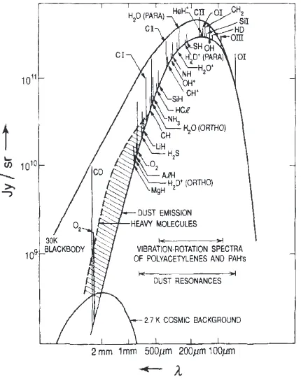
typical dense interstellar dust cloud is shown in Fig. 1.2 where we can see the various
continuum and spectral emission lines. Such clouds can have temperatures between 10–100 K heated by the optical and infrared light from embedded hot stars. These
temperatures correspond to the excitation energies of many atomic fine-structure and molecular rotational transitions.
Figure 1.2: A schematic presentation of some of the spectral content in the submillimeter/far-IR band for an interstellar cloud (Radiated energy versus wave-length). The spectrum includes dust continuum emission, molecular rotation lines and atomic fine-structure line emissions superimposed on the microwave background radiation. Figure reprinted from [3]
1.1.2
Detector technology
The richness of the many phenomena observable in the submm/far-IR range drives the development of new and more sensitive detector technologies for large-scale arrays.
for this task. The two main types of detectors used today are bolometric and
pair-braking detectors. Bolometric detectors work on the basis of sensing small changes in the temperature of a small superconducting island while pair braking detectors sense
the change in the number of quasiparticles that are created when photons break Cooper pairs.
The most sensitive type of bolometric detector today is the transition-edge sen-sor (TES) [5, 6, 7]. These sensen-sors use the very steep resistive transition from the
superconducting state to the normal state. By biasing the detector at the transition, a weak radiation signal can produce a large change in the resistance. For a stable
bias point, voltage biasing is used and the current flowing through the resistor is
measured by using a superconducting quantum interference device (SQUID) which amplifies the signal. In this technology each pixel needs its own SQUID and readout
channel. SQUIDs require a relatively complex fabrication process (up to 10 levels of lithography), and this increases cost, especially for large arrays.
One example of a pair-breaking detector is the superconducting tunnel junction (STJ) detector [8]. These use a superconductor-insulator-superconductor (SIS)
junc-tion that has a very thin insulator barrier in between two superconducting contacts. Due to quantum mechanical tunneling a small current exists when the junction is
biased with a constant voltage. When photons break Cooper pairs inside the super-conductor they create quasiparticles which can tunnel across the barrier and increase
the current. A drawback is that since the Cooper pairs can also tunnel – this is the Josephson effect – the pair current must be suppressed using an aligned magnetic
field. This can be difficult for large arrays since the magnetic field required can vary for different junctions due to variation in the barrier properties.
Today, submillimeter/far-IR astronomy has reached a point where ground-based
detectors have reached background-noise-limited operation where the photon noise from the atmosphere dominates over the intrinsic detector noise. Therefore, to
1990 1995 2000 2005 2010 2015 100
101 102 103 104 105
Year
Number of Detectors
CCAT
Scuba II
CSO
UKT14
Sharc I Scuba
Mambo I Bolocam
Mambo II
Sharc II Laboca Apex SZ
SPT (initial) Scuba II (initial)
ACT
SPT MUSIC (MKIDcam)
Figure 1.3: The growth of submillimeter detector array size as a function of time has followed an exponential trend over the past two decades, with a growth rate exceeding a factor of 2 every two years. Blue points represent existing (or obsolete) instruments; the green points are projections. MUSIC stands for “multiwavelength submillimeter kinetic inductance camera”. Figure reprinted from [9]
plane arrays with pixels of order 104–106 are required for major progress.
Submillime-ter and far-IR bolometric arrays have been growing exponentially in a Moore’s law fashion, doubling in size every 20 months [9], and have reached pixel counts as high
as 104 in the SCUBA-2 instrument [10, 11] (see Fig. 1.3). However, further progress
has been hampered by complicated and costly fabrication and readout electronics,
es-pecially the need for complex cryogenic SQUID-based multiplexing circuits. This has driven the need for simplified alternative detector designs suitable for high packing
1.2
Microwave kinetic inductance detectors
Microwave kinetic inductance detectors (MKID) [12, 13] offer a potential solution for large-scale arrays. These arrays can be easily made with a single layer of
supercon-ducting metal film deposited on a silicon substrate and pattered using conventional optical lithography. Furthermore, MKIDs are inherently multiplexable in the
fre-quency domain, allowing∼103 detectors to be read out using a single coaxial trans-mission line and cryogenic amplifier, and room-temperature electronics, drastically
reducing cost and complexity.
MKIDs are a type of pair-breaking detector, in which the absorbed radiation en-ergy breaks Cooper pairs inside a thin superconducting film resulting in a change of
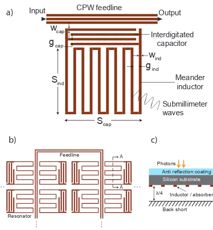
the kinetic inductance. The film is cooled to T Tc and has a superconducting energy gap 2∆ ≈ 3.52kBTc. Photons with sufficient energy (ν ≥ 2∆/h) can break one or more Cooper pairs and create extra quasiparticles as shown in Fig 1.4 (a). These recombine with a time constant τqp ≈10−6–10−3 s depending on the material. During this time, the quasiparticle density increases by a small amountδnqp above its thermal equilibrium value, resulting in a change δZs in the surface impedance of the film (Zs = Rs+jωLs). Although δZs is quite small, it can be sensitively measured if the film is part of a resonator structure (Fig 1.4 (b)). The resonator is weakly
coupled to a transmission line which is used to read out the resonator. Changes inLs and Rs affect the frequencyfr and quality factor Qr of the resonance feature, respec-tively, changing the amplitude and phase of a microwave probe signal (tuned on the resonance frequency) transmitted through the feedline (Fig 1.4 (c) and (d)). Both
of these signals can be read out and are referred to as the frequency direction and dissipation direction signals. A cryogenic SiGe transistor amplifier or a high electron
mobility transistor (HEMT) amplifier followed by homodyne mixing at room temper-ature is used to readout these signals [12]. In an array of MKIDs, all the resonators
...
...
...
...
Photons
Anti reflection coating
Silicon substrate
Inductor / absorber
λ/4
Back short
A
A
f)
Feedline
Resonator
Tr
ansmission (dB)
Cooper pair
Phase
R C L
e)
a) c)
b) d)
r f r f
r
f f
Feedline
using digital techniques [14, 15]. Fig. 1.4 (e) shows a schematic illustration of a
section of an MKID array described in chapter 4 and 5 of this thesis. Although the resonators are lumped-element in this case (called lumped-element kinetic inductance
detector or LeKID), there are also distributed versions of MKIDs. Fig. 1.4 (f) shows the radiation coupling mechanism to a LeKID. Photons are directly absorbed inside
the meandered inductor section.
The fundamental limit to the sensitivity of an MKID is determined by the random
generation of quasiparticles by pair-breaking thermal phonons and their subsequent recombination, resulting in generation-recombination noise. Fortunately, this noise
is exponentially suppressed at lower temperatures by the Boltzmann factor e−∆/kBT. However, in practice MKIDs are still limited by other nonfundamental sources of noise, such as amplifier noise and capacitor noise due to two-level system (TLS)
fluctuators in amorphous dielectrics. Constant progress in development of lower-noise amplifiers has been very beneficial for MKIDs [16]. TLS noise can be significantly
reduced as will be shown in chapter 3 of this thesis, but the remaining noise is still an issue.
MKID arrays are being developed for astronomy at a wide range of wavelengths from millimeter waves to x-rays [17, 18, 19, 20]. Other applications of superconducting
Chapter 2
Principles of kinetic inductance
detectors
In this chapter we will review the basics of the operation of a microwave kinetic
inductance detector (MKID). We will explain the principle of detection going through the chain of signal starting from perturbations to the complex conductivity of a
superconductor to the final detection of a voltage. The calculations and the formulae in this chapter will be used later throughout the rest of the thesis.
2.1
Principle of detection
2.1.1
Surface impedance and complex conductivity of
super-conductors
In a superconductor at zero temperature, all the electrons are bound into pairs called
Cooper pairs. This happens due to the interaction between the lattice and the elec-trons which creates a weak attractive force that binds the elecelec-trons into pairs.
Ac-cording to BCS theory [26] the pairs have a binding energy of
where Tc is the critical temperature above which superconductivity vanishes and ∆0
is the energy gap of the superconductor. The binding energy is quite weak, of the order of meV, and thermal energy can easily break the pairs. Thus at a nonzero
temperatureT < Tcsome of the pairs will be broken into quasi single electrons called quasiparticles. The quasiparticle density per unit volume is given by
nqp = 4N0
Z ∞
∆
E
√
E2−∆2f(E)dE (2.2)
where ∆ is the nonzero temperature gap and f(E) = 1/(1 +eE/kBT) is the Fermi-Dirac distribution for the quasiparticles in thermal equilibrium. ForT Tc we have ∆≈∆0 and
nqp ≈2N0 p
2πkbT∆0e
−∆0
kB T . (2.3)
Here N0 is the single-spin density of electron states at the Fermi energy, which for
aluminum is 1.72×1010 µm−3 eV−1 [12]. From Eq. 2.3 we can see that as T −→0,
nqp −→0 in an exponential manner. Because of the energy gap, Cooper pairs carrying electrical current cannot easily get excited into a higher energy state which means
they cannot scatter like normal electrons. Therefore, superconductors show zero DC resistance below their critical temperature Tc. However, they do show nonzero resistance and inductance in the case of AC fields. This is because the electromagnetic field can penetrate inside the superconductor over a length of λ (the penetration
depth) due to the Meissner effect. When T > 0 the existence of normal electrons (quasiparticles) introduces resistive loss to the AC field. On the other hand the
Cooper pairs store energy in the form of kinetic and magnetic energy and introduce a purely inductive impedance, because they lag the electric field due to their inertia.
The combined effect of the quasiparticles and the Cooper pairs produces a complex surface impedance
Zs =Rs+jXs . (2.4)
2∆/h) the complex conductivity σ =σ1−jσ2 is given by: σ1 σn = 2 ~ω Z ∞ ∆
E2+ ∆2+ ~ωE
√
E2−∆2p
(E+~ω)2−∆2 h
f(E)−f(E+~ω)
i dE (2.5) σ2 σn = 1 ~ω
Z ∆+~ω ∆
E2+ ∆2 − ~ωE
√
E2−∆2p∆2−(E− ~ω)2
h
1−2f(E)idE (2.6)
where σn = 1/ρn is the normal-state conductivity of the superconductor just above Tc. In the temperature range T Tc, σ1 σ2. In the case where kBT ∆0 and ~ω∆0, these two integrals can be simplified [28] to
σ1(nqp) σn = 2∆0 ~ω nqp N0 √
2πkBT∆0
sinh(ξ)K0(ξ) (2.7)
σ2(nqp) σn
= π∆0 ~ω
h
1− nqp
2N0∆0
1 +
r
2∆0
πkBT
e−ξI0(ξ) i
(2.8)
ξ = ~ω 2kBT
, (2.9)
whereI0 andK0 are the zeroth-order modified Bessel functions of the first and second
kind, and where we have used Eq. 2.3 to write these in term of nqp. Here nqp is the total quasiparticle density due to thermal generation and pair breaking by photons. The last step is important because we can now directly see that both σ1 and δσ2 =
σ2−σ2(0) are proportional to nqp. This is the basic detection mechanism of MKIDs:
quasiparticles that are created by absorption of photons or thermal generation in the
superconductor can be sensed through perturbations in the complex conductivity. From Eq. 2.7 and Eq. 2.8 it can be shown that the fractional changes in σ1 and σ2
are equal to fractional changes in nqp 1:
δσ1
σ1
= δnqp nqp
(2.10)
δσ2
σ2−σ2(0)
= δnqp nqp
(2.11)
On the other hand, a perturbation in the complex conductivity results in a
per-1An underlying assumption here is that the perturbation in the quasiparticle distribution function
turbation in the complex surface impedance of the film in the following way: In the
case when the film thickness t is much smaller than the effective penetration depth λef f and t is smaller than the electron mean free path `e 2, we can simply write [28]
Zs= 1
σt (2.12)
= 1
(σ1−jσ2)t
(2.13)
≈ σ1
tσ2 2
+j 1 tσ2
. (2.14)
Therefore, from Eq. 2.12 a fractional perturbation in conductivity is related to the
fractional perturbation in surface impedance as
δZs Zs
=−δσ
σ . (2.15)
If we consider perturbation around zero temperature, we have Zs(0) = jXs(0) and σ(0) =−jσ2(0), and if we assume σ1 σ2 we can write, to first order:
δRs Xs(0)
= δσ1 σ2(0)
(2.16)
δXs Xs(0)
=− δσ2
σ2(0)
. (2.17)
Using Eq. 2.10 and Eq. 2.11 the above two equations can be written in terms of perturbations in quasiparticle density:
δRs Xs(0)
= S1(ω) 2N0∆0
δnqp (2.18)
δXs Xs(0)
= −S2(ω) 2N0∆0
δnqp (2.19)
where S1(ω) and S2(ω) are defined in the limit ~ω, kBT ∆0 as
S1(ω)∼=
2 π
r
2∆0
πkBT sinh(ξ)K0(ξ) (2.20)
S2(ω)∼= 1 + r
2∆0
πkBT
e−ξI0(ξ), (2.21)
and
β= S2(ω) S1(ω)
= δσ2 δσ1
= |δXs| δRs
(2.22)
is the ratio of the two perturbations. This ratio is important because it determines
which response is stronger. It is also useful when comparing the observed response ratio in measurements to theory. Furthermore, it is convenient to express the
pertur-bations in parameters in terms of δnqp because as we will see later the perturbations in the incident optical power on the detector δPo directly determinesδnqp.
The changes in the surface impedance can be very sensitively measured using a
resonant circuit made from the superconductor. The concept is illustrated in Fig. 1.4 where the RLC circuit represents the detector. As photons break Cooper pairs
inside the detector, the resonance frequencyfr and the quality factorQrof the circuit changes. This change can be probed by weakly coupling the resonator capacitively or
inductively to a transmissionline called a “feedline”. By sending a microwave probe signal on the feedline tuned on the resonance frequency, the complex amplitude of
the signal S21 changes by δS21 every time photons hit the detector. In the following
sections we will calculate how δS21 is related to the changes in the incident optical
power δPo. We start by examining the quasiparticle lifetime and its steady-state value.
2.1.2
Quasiparticle lifetime
recombination probability is higher. As the temperature is reduced the thermally
generated quasiparticles reduce and τqp increases. However, it has been experimen-tally observed [29, 30, 31] that the lifetime saturates at a maximum level τmax for nqp .n∗ ≈100 µm3 and has the form
τqp−1 =τmax−1 +Rnqp . (2.23)
R= 1/n∗τmax is called the recombination constant and is theoretically given by [32]
R= (2∆)
2
2N0τ0(kBTc)3
(2.24)
where τ0 is the material-specific electron-phonon interaction time.
The quasiparticle population is governed by generation and recombination
pro-cesses. These are thermal quasiparticle generation, excess quasiparticle generation, and quasiparticle recombination. We can write
dnqp
dt = Γgen−Γrec (2.25)
where Γgen and Γrec are the generation and recombination rates. To calculate the steady-state populationnqp we can set the generation and recombination rates equal. The generation rate consists of two terms
Γgen = Γth+ Γe (2.26)
where Γthis the thermal generation rate, and Γe is the excess quasiparticle generation rate from optical power incident on the detector and the readout power. We can write
Γe= Γo+ Γa= ηoPo ∆0
+ηaPa ∆0
(2.27)
quasipar-ticles, Po is the incident optical power, and Pa is the absorbed readout power inside the resonator. For the readout power efficiency we can write an expression
ηa= Nread
qp ∆ τqpPaqp
(2.28)
where Nqpread is the quasiparticle population created due to the readout and where Pqp
a =χqpPa is the absorbed power by the quasiparticles due to readout andχqp ≤1 determines the proportionality.
The recombination rate depends on the total quasiparticle population and can be
written as
Γrec = 1 2Nqp(τ
−1
max+τ
−1
qp ) = Nqp(τmax−1 + 1
2Rnqp) (2.29) whereNqp =nqpV is the total quasiparticle population in the superconducting volume V.
The thermal generation rate Γthis equal to the recombination rate at the thermally generated quasiparticle density at temperature T
Γth = Γrec(nth(T)) (2.30)
where nth is determined from Eq. 2.3. However, nth can be made sufficiently small at low temperatures that it can become negligible. Solving for nqp in Eq. 2.25 at steady-state we get
nqp =n∗
p
1 + 2Γeτmax/N∗−n∗ (2.31) where N∗ =V n∗. The lifetime is given by using Eq. 2.31 in Eq. 2.23:
τqp =
τmax
p
1 + 2Γeτmax/N∗
. (2.32)
re-sponse to a perturbation in the incident optical power δPo:
δNqp = ∂Nqp ∂Po
δPo = ∂Nqp ∂Γe
∂Γe ∂Po
δPo . (2.33)
The first factor can be calculated from Eq. 2.31 and is equal to ∂Nqp/∂Γe =τqp. The second factor can be calculated from Eq. 2.27 and is ∂Γe/∂Po =ηo/∆0. Therefore,
δNqp = ηoτqp
∆0
δPo . (2.34)
Next we will examine the electrical resonant circuit that is used to sense the changes in the surface impedance.
2.2
Resonator circuit
In the previous sections we evaluated how a change in quasiparticle density affects the
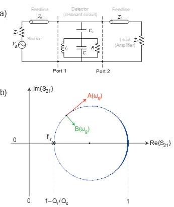
surface impedance. Here we will examine the resonator circuit that is used to sense the changes in the surface impedance. Fig. 2.1 (a) shows an equivalent circuit diagram
for the resonator and readout mechanism. The resonator which is the RLC tank circuit is coupled capacitively to a feedline. A microwave voltage generator produces
a signal that is transmitted through the feedline past the resonator and is amplified with an amplifier. When the signal is tuned near resonance the complex amplitude
of the signal is affected by the resonator. The forward complex transmissionS21from
port 1 to port 2 is shown in Appendix A to be
S21 ≈1−
Qr Qc
1 1 + 2jQrx
(2.35)
x= ω−ωr ωr
(2.36)
L
C
C
cZ
0R
V
gPort 1 Port 2
Z
0Z
0Z
0Feedline Detector Feedline
(resonant circuit)
Load (Amplifier) Source
0 1
0
1–Qr/Qc
Re{S } 21
Im{S } 21
f
r*
A(ωg)
B(ωg)
a)
b)
Figure 2.1: (a) Equivalent circuit illustration of a superconducting resonator coupled capacitively to a transmission line (“feedline”). The load impedance Z0 represents
the amplifier’s input impedance. The voltage source and its impedance represent the microwave generator used to read out the resonator. (b) The circular trajectory of the complex transmission S21 as a function of frequency for the circuit in (a) is
quality factor. These are related by (see Appendix A)
1 Qr
= 1 Qc
+ 1 Qi
. (2.37)
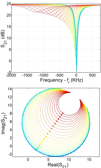
The transmission S21 traces a clockwise circle in the complex plane as the frequency
is increased from below the resonance to above the resonance. This is shown in Fig. 2.1 (b). Far away from resonance S21 −→ 1. On resonance S21 reaches a minimum
value of min(|S21|) = 1−
Qr Qc
. The value of Qr can be determined from the resonance
bandwidth Qr = fr 2∆νr
where 2∆νr is defined as the frequency bandwidth spanning half the resonance circle in Fig. 2.1 (b). The value of Qc and Qi can be determined from
Qc =
Qr 1−min(|S21|)
(2.38)
Qi =
Qr min(|S21|)
. (2.39)
In practice however, the resonance circle will be affected by the measurement
read-out circuit. Cable delay will cause the loop to become smaller, crossing itself, and impedance mismatch between the feedline and the load and source impedances will
rotate the loop. These effects can be taken out by using a resonance fitting code.
When photons are absorbed in the resonator the surface impedance of the circuit changes which causes a change in the resonance frequency and quality factor. This
in turn changes the complex transmission S21 which is measured. We can calculate
the perturbation in S21 as a function of perturbations in fractional frequency x and
Qi. For slow perturbations compared to the resonance response time we can write
where A(ω) and B(ω) are
A(ω) = ∂S21
∂x = 2jQc 1−S21(ω)
2
(2.41)
B(ω) = ∂S21 ∂Q−i 1 =
1
2jA(ω) (2.42)
and δx(t) = δfr(t) fr
. The directions of the vectors A(ω) and B(ω) are tangent and perpendicular to the resonance circle as shown in Fig. 2.1 (b). These two directions
are commonly referred to as the frequency and dissipation (or phase and amplitude) directions, respectively. For fast perturbations with frequency ν the resonator
ring-down response should also be included which acts as a low-pass filter when ω =ωr. To include this effect we switch to the frequency–domain representation of Eq. 2.40
δS21(ν) =
A(ω)δx(ν) +B(ω)δQ−i 1(ν)ζ(ν) (2.43)
where
ζ(ν) = 1 1 +jν/∆νr
. (2.44)
However, for our situation the perturbation in the signal is usually much slower than the resonator response time andζ −→1.
To follow the notation of Zmuidzinas et al. [13] we define the following variables to rewrite Eq. 2.43 in terms of these:
φg = tan−12Qrx (2.45)
is the phase angle;
χc =
4QcQi (Qc+Qi)2
= 4Q
2
r QcQi .
1 (2.46)
and
χg(ω) =
1 1 + 4Q2
rx2
.1 (2.47)
is the generator detuning efficiency which is maximized when the generator frequency is tuned on resonance, ω =ωr. Using the above three definitions we can rewrite Eq. 2.41 and Eq. 2.42 as
A(ω) =jQi 2 χcχge
−2jφg (2.48)
B(ω) = Qi 4 χcχge
−2jφg . (2.49)
We can now rewrite Eq. 2.43 using the above two equations
δS21(ν) =
1
4χcχgQie
−2jφg2jδx(ν) +δQ−1 i (ν)
ζ(ν) +δSa(ν). (2.50)
We have added a noise term δSa(ν) = δIa(ν) +jδQa(ν) representing the amplifier’s additive white noise which has a noise power spectral density of
PSD(δIa) = PSD(δQa) = kBTa 2Pfeed
(2.51)
whereTais the amplifier noise temperature andPfeedis the microwave generator power
incident on the feedline. Note that part ofPfeedis absorbed inside the resonator which
is equal to
Pa= (1− |S11|2− |S21|2)Pfeed =
χcχg
2 Pfeed ≤ 1
2Pfeed . (2.52)
Another important noise source that must be included in Eq. 2.50 is the excess two-level system (TLS) frequency noise. This noise is intrinsic to the resonator and
causes a jitter in the resonance frequency that is characterized by the fractional frequency noise power spectral densitySTLS(ν) corresponding to fluctuations in x. It
frequency perturbation term. We can rewrite Eq. 2.50 to include it as follows:
δS21(ν) =
1
4χcχgQie
−2jφg2jδx(ν) + 2δx
TLS(ν) +δQ−i 1(ν)
ζ(ν) +δSa(ν). (2.53)
2.3
Resonator response
We can now start to calculate the relation between quasiparticle perturbations δnqp and resonator circuit transmission perturbations δS21. We start by calculating the
perturbation in resonance frequency and quality factor. The resonance frequency in Fig. 2.1 (a) is simply (see Eq. A.22)
fr = 1
2π√LC . (2.54)
A perturbation in the inductance is related to a perturbation in frequency as
δx= δfr fr
= −δL
2L . (2.55)
We can write the total inductanceL as the sum of the geometric inductance and the kinetic inductance L=Lm+Lki. Only the kinetic inductance is perturbed so we can write
δx = −δLki
2(Lki+Lm) =− α 2
δLki Lki =−
α 2
δXs
Xs , (2.56)
where
α= Lki Lki+Lm
(2.57)
is defined as the kinetic inductance fraction. Using Eq. 2.19 in Eq. 2.56 we can now
relate δx to δnqp:
δx= αS2(ω) 4N0∆0
We can follow the same logic for perturbations in the internal quality factor. We start
by writing
Q−i 1 = R
ωL . (2.59)
A perturbation in the resistance is related to a perturbation in Q−i 1 as
δQ−i 1 = δR ωL =α
δR ωLki
=αδRs Xs
. (2.60)
Using Eq. 2.18 in the above equation we can now relate δQ−i 1 to δnqp as
δQ−i 1 = αS1(ω) 2N0∆0
δnqp . (2.61)
Note that we can write a similar relation between the internal quality factor Qi and the total quasiparticle density nqp
Q−qp1 =χqpQ−i 1 =
αS1(ω)
2N0∆0
nqp (2.62)
where the factorχqp ≤1 accounts for the portion of the internal resonator loss that is due to quasiparticles. Other loss mechanisms like radiation into free space and TLS loss (see Chapter 3) can contribute toQ−i 1 but are not affected by quasiparticles.
Using Eq. 2.34 together with Eq. 2.58 and Eq. 2.61 it is convenient to define the fractional frequency responsivity Rx and the loss responsivityRQ−1
i as
Rx = δx δPo
= αS2(ω)ηoτqp 4N0∆20V
(2.63)
RQ−1 i =
δQ−i 1 δPo
= αS1(ω)ηoτqp 2N0∆20V
. (2.64)
We will later use the ratio between these two responses in bath temperature sweep
We can combine Eq. 2.58, Eq. 2.61, and Eq. 2.62 with Eq. 2.53 to obtain a
relation between δS21 and δnqp
δS21(ν) =
1
4χcχgχqp e
−2jφg1 +jβ(ω)ζ(ν)δnqp nqp +j e−2jφgχcχg
2 Qi ζ(ν)δxTLS+δSa(ν). (2.65) Finally, using Eq. 2.34 we can write the relationship between δS21 and the optical
power δPo as
δS21(ν) =
1
4χcχgχqp e
−2jφg1 +jβ(ω)ζ(ν) ηoτqp ∆0Nqp
δPo +j e−2jφgχcχg
2 Qi ζ(ν)δxTLS+δSa(ν). (2.66) From the above equation it is easy to write expressions for the frequency and
dissi-pation direction responsivities (gains):
Re(δS21)
δPo
= ηoχcχqpτqp 4Nqp∆0
(2.67)
Im(δS21)
δPo
= β(ω)ηoχcχqpτqp 4Nqp∆0
(2.68)
where we have assumed that ζ(ν) = 1. We will make this assumption from here on
since the astronomical signals observed in the submillimeter and far-IR have very slow variations in time. We can see that the responsivity in the frequency direction
is a factor ofβ(ω) larger than the dissipation direction. This is a potential advantage for the frequency response. However, because of the extra TLS noise in this direction
2.4
Resonator sensitivity
In order to calculate the sensitivity of an MKID resonator we need to consider the noise sources contributing to the signal. These could be intrinsic noise like the TLS
noise (see Chapter 3), thermal quasiparticle generation shot noise, quasiparticle re-combination shot noise, or extrinsic noise like the photon shot noise in the optical
power. We will calculate the noise equivalent power (NEP) at the input of the detector for each of these noise sources.
The power spectral density of shot noise in the generation rate Γth from thermal generation of quasiparticles is given by [13]
SΓth = 2Γth =Nth(τ
−1
max+τ
−1
th ) (2.69)
whereNth is the thermal quasiparticle population at temperatureT when the system is in thermal equilibrium (see Eq. 2.3), and τth−1 =Rnth+τmax−1 is the lifetime. The power spectral density of shot noise in the recombination rate Γr from the recombi-nation of all quasiparticles is given by
SΓr = 2Γr =Nqp(τ
−1
max+τ
−1
qp ). (2.70)
Both the above power spectra are defined for double-sided noise. With some calcula-tion it can be shown [13] that the contribucalcula-tion of the above generacalcula-tion and
recombi-nation terms to the noise equivalent power is
NEP2g−r = 2Nth(τmax−1 +τ
−1
th ) +Nqp(τmax−1 +τ
−1
qp )
∆0
ηo
2
(2.71)
where the factor of 2 is to account for noise in positive and negative frequencies
After some calculation we can estimate the recombination NEP as
NEPr ≈2
s
Po∆0
ηo . (2.72)
The photon noise equivalent power intrinsic to the incident optical signal is given by [13]
NEP2ph = 2Pohν(1 +n0) (2.73)
where n0 = 1/(ehν/kBT −1) is the photon occupation number and ν is the photon
frequency. The factor of two is for single-sided noise.
The amplifier noise contribution to NEP can be calculated by using Eq. 2.51
together with Eq. 2.67 or Eq. 2.68. The amplifier NEP contribution to the dissipation direction signal and to the frequency direction signal are:
NEPampdiss =√2× r
kBTa 2Pfeed
× δPo
Re(δS21)
= 4Nqp∆0 ηoχcχqpτqp
r
kBTa Pfeed
(2.74)
NEPampfreq =√2× r
kBTa 2Pfeed
× δPo
Im(δS21)
= 4Nqp∆0 β(ω)ηoχcχqpτqp
r
kBTa Pfeed
(2.75)
where the factor of √2 is for single-sided NEP.
The TLS NEP contribution to the frequency direction signal can be calculated
by using Eq. 2.63 together with the TLS fractional frequency noise spectral density STLS:
NEP2TLS = 2STLS R2
x
= 2 4N0∆
2 0V
αηoS2(ω)τqp
!2
STLS . (2.76)
The factor of 2 is for single-sided NEP assuming that STLS is double-sided. Now
dissipation signal directions:
NEP2diss= 2Pohν(1 +n0) + 2
Nth(τmax−1 +τth−1) +Nqp(τmax−1 +τqp−1)
∆0
ηo
2
+ 4Nqp∆0 ηoχcχqpτqp
!2
kBTa Pfeed
(2.77)
NEP2freq = 2Pohν(1 +n0) + 2
Nth(τmax−1 +τ
−1
th ) +Nqp(τmax−1 +τ
−1
qp )
∆0
ηo
2
+ 4Nqp∆0 β(ω)ηoχcχqpτqp
!2
kBTa Pfeed
+ 2 4N0∆
2 0V
αηoS2(ω)τqp
!2
STLS (2.78)
where the above NEPs are single-sided.
2.4.1
Photon noise limited condition
It is useful to calculate the condition when NEPTLS ≤ NEPph; i.e., photon
noise-limited operation of the detector. We assume that the optical illumination power
is high such that Γeτmax/N∗ 1 which is the case for ground-based submillime-ter astronomy. Using Eq. 2.32 and Eq. 2.27 this gives a quasiparticle lifetime
τqp ≈
p
τmaxn∗∆0V /2ηoP0. We can further use Eq. 2.24 to substitute n∗τmax by 2N0τ0kBTc/F2 where F = 2∆0/kBTc ≈ 3.52. Doing so we can set the required condition as
NEP2TLS = 32 ∆
2
0F2N0V Po∆0
α2S
2(ω)2τ0kBTcηo
STLS < 2Pohν(1 +n0) = NEP2ph . (2.79)
Rearranging the above we get
STLS <
hν(1 +n0)α2S2(ω)2τ0ηo 8 ∆2
0F3N0V
. (2.80)
We can use the above equation to evaluate whether the TLS noise in a certain device
for ground-based submillimeter astronomy at λ = 350µm assuming an atmospheric
temperature of 270 K gives n0 ≈ 6. For a typical MKID, if we assume a resonator
active inductor volume V = 1000 µm3 made from aluminum (T
c = 1.2 K), electron-phonon interaction time τ0 = 438 nsec [32], a resonance frequency fr = 5 GHz, and S2 ∼2.5, we get an upper limit for single-sided TLS fractional frequency noise power
spectral density of
Chapter 3
Two-level system (TLS) noise
reduction for MKIDs
In this chapter we will discuss the details of a technique for reducing excess frequency
noise in superconducting microwave resonators. Intrinsic noise in the form of an excess resonance frequency jitter exists in planar superconducting resonators that are made
on dielectric substrates – usually crystalline silicon or sapphire [12, 33]. This noise can be a serious problem when these resonators are used as kinetic inductance detectors
and can limit the sensitivity that is needed for astronomical observations. These resonators are also of interest in other applications including readout multiplexing
of transition edge sensors [24], parametric amplifiers [25], and quantum computation [34], which could benefit from lower noise resonators. As we conclusively show in
this chapter, this noise is due to fluctuations of the resonator capacitance [35]. In turn, the capacitance fluctuations are thought to be driven by two-level system (TLS)
fluctuators in a thin layer on the surface of the device [36].
We will first give an introduction to TLS and their effects on resonators, and then will describe a novel design aimed for reducing TLS noise. We will show measurements
3.1
Introduction to two-level systems
Amorphous solids have very different thermal, acoustic, and dielectric bulk properties at low temperatures as compared to crystalline solids. In 1972 Phillips [37] and
Anderson [38] introduced a model that successfully explains these properties observed in experiments. Their model attributes these properties to the presence of quantum
two-level systems (TLS) in amorphous materials. TLS arise due to the disordered structure of amorphous materials because one or a group of atoms can move from one
configuration to another configuration corresponding to two local potential energy minima. The atoms do this by quantum tunneling over an energy barrier to the other
state. The difference between the energies in the two states arises from an energy difference between the two chemical bond configuration. The tunneling behavior of
TLS can be quantum mechanically described as a particle in a double-potential well. Because of the random nature of these materials the energy minima and the barrier
energy height are assumed to be random in this model, leading to a random, uniform distribution of TLS energy splittings. The atoms have an electric dipole moment
which makes them electrically active each time they tunnel. These dipole moments can couple to electric fields, and therefore can affect the dielectric constant of the
material and introduce additional dielectric loss. If TLS exist inside a microwave resonator, the electric fields from the resonator will couple to the dipoles of the
TLS and power will be stolen from the resonator and turned into loss reducing the resonance quality factor.
The existence of TLS can also produce excess frequency noise in superconducting
resonators. This is due to the random nature of TLS tunneling events causing a random fluctuation in the dielectric constant. The fluctuations could be caused by
different mechanisms. These could be random emission or absorption of phonons. Another possibility could be the random tunneling of neighboring TLS creating a
noise in resonators which can significantly impact the performance of MKIDs.
For these reasons it is important to evaluate the effect of TLS in superconducting resonators, and to find ways to reduce the loss and noise. Below we will describe the
effects of TLS loss and noise on resonators in more detail.
3.2
Resonator loss from TLS
As explained above, TLS exist inside amorphous materials. Significant studies have
been done to determine the effect and amount of TLS loss in superconducting qubits for quantum computing [39, 40] where low loss is essential for long coherence times,
and in superconducting microwave resonators used for MKIDs [28, 41, 42] where high Qs are desirable. The details of the theory relevant to the case of MKIDs were carried
out in Gao’s PhD thesis work [28].
TLS have dipole moments that can couple to electric fields, and therefore can
contribute an amount TLS(f, T) to the real (reactive) and imaginary (dissipative)
parts of the dielectric constant of the TLS-hosting material. First we look at the
effect of the imaginary part.
In the case of weak electric fields |E| Ec (or low microwave powers P Pc) whereEc and Pc are a critical field and power, the TLS contribution to the dielectric loss tangent δ in a bulk material is given by [28, 43]:
δTLS(f, T) =
Im{TLS(f, T)}
Re{} =δ0tanh
hf
2kBT
, (3.1)
where δ0 represents the TLS-induced loss tangent at zero temperature and weak
electric fields, and is proportional to the density of TLS per unit volume and energy. The hyperbolic tangent factor comes from the thermal occupation probabilities of
limit where kBT hf, the excited state is well occupied and stimulated emission cancels much of the absorption, leading to δTLS(f, T)∝hf /kBT [13]. For the case of high microwave powersP, it can be shown [44, 28, 43] that the loss tangent becomes
power dependent
δTLS(P) =
δTLS(P = 0) p
1 +P/Pc
(3.2)
where Pc is the critical power for TLS saturation and is related to the tunneling transition strength. This power dependence has been experimentally observed in superconducting resonators [28, 45, 40] and in superconducting qubits [39]. For the
case of superconducting resonators, the internal resonator loss due to TLS (1/QTLSi ) is related to the loss tangent by
1 QTLS
i
=− R
VhIm{TLS}| ~
E(~r)|2d~r
R
V |E(~~ r)|2d~r
=FTLSδTLS(f, T) (3.3)
where
FTLS = R
Vhh ~ E(~r)2d~r
R
V ~E(~r)
2d~r =
we h
we . (3.4)
HereFTLS is a filling factor that accounts for the fact that the TLS hosting material
with h and volume Vh may only partially fill the resonator volume V, and is equal to the ratio of the electric energy we
h stored in the TLS hosting volume to the total electric energy we stored in the resonator [28]. For the case when P Pc, we can write
1 QTLS
i
=FTLSδ0tanh
hf
2kBT
. (3.5)
TLS also affects the reactive part of which manifests itself by a resonance
fre-quency shift in resonators. The change in the reactive part of epsilon is related to a change in resonance frequency
∆fr fr
=−FTLS
2
Re{TLS}
Re{} (3.6)
=− R
VhRe{TLS}| ~
E(~r)|2d~r
The shift can be calculated by using the Kramers-Kroenig relationship between the
real and imaginary parts of the dielectric constant and is equal to
∆fr fr
= fr(T)−fr(T = 0) fr
= FTLSδ0 π
"
ReΨ1 2 +
1 2πi
hf kBT
−ln hf kBT
#
, (3.8)
where Ψ is the complex digamma function [28, 43], and has negligible power
depen-dence.
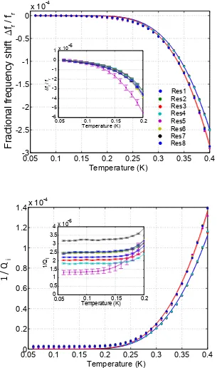
Equations 3.5 and 3.8 can be used to experimentally diagnose the presence of TLS in resonators and to quantify its amount: for a certain resonator we can sweep
the bath temperature T over a wide range recording fr(T) and Qi(T). We can then use equations 3.5 and 3.8 along with the Mattis–Bardeen equations describing the
quasiparticle-induced change in fr and 1/Qi (Eq. 2.56 and Eq. 2.60) to fit to the data and extract the FTLSδ0 factor. FTLS can be determined numerically for the
specific resonator geometry at hand if the specific location and geometry of the TLS hosting material are known. Also, knowledge of the distribution of the electric field
in the resonator is needed. This has been demonstrated [28] for CPW resonators where a thick artificial layer of dielectric (e.g., SiNx or SiO2) was deposited on the
CPW resonator so that FTLS could be easily determined from EM simulations. The
frequency shift and the internal quality factor were shown to agree with the predictions
of Eq. 3.8 and Eq. 3.5. However, if the exact location and geometry of the TLS hosting material is not known, it would be difficult to diagnose the type of material
hosting the TLS and to determine its loss tangent. This problem becomes more evident in the case of resonators that are fabricated on a crystalline substrate (like
Si or sapphire) and do not use any deposited amorphous films. In these resonators even though amorphous materials are not used, a small amount of TLS loss and TLS
frequency shift is still observed, but the location of the TLS are not evident. Gao et al. showed that in these resonators a thin (few nm) layer of TLS hosting material on the
that the corresponding scaling ofs−1 in TLS frequency shift can only be explained by
a surface distribution and not a bulk distribution of TLS. This is because for a bulk distribution the filling factor FTLS is fixed while for a 2D distribution it reduces as
∼s−1 as the CPW becomes wider. For TLS loss, Barends et al. [47] showed that by
removing part of the silicon substrate in the CPW slot regions with high electric field,
FTLS can be reduced resulting in lower TLS loss. This can be understood by noting in
Eq. 3.3 that the TLS from different locations in the resonator contribute to the loss
with a scaling of |E(~~ r)|2. Therefore, TLS located in the high-field regions are more
important and should be considered in the resonator design process. There are many
candidates for the TLS surface layer material in superconducting resonators. Native oxide layers from metals like Al and Nb, or native oxides from crystalline substrates
like Si and sapphire can all be host material for TLS. Defect impurities or chemical residues left from fabrication processing steps like etching or other processes can also
be responsible.
3.3
Resonator frequency noise from TLS
MKID resonators consistently show excess frequency noise [12, 33, 48, 42, 36]. The noise is a small time-dependent jitter of the resonance frequency fr characterized by the frequency noise power spectral density Sδfr in units of Hz
2/Hz, or the fractional
frequency noise spectral density Sδfr/fr in units of 1/Hz. This noise corresponds to fluctuations in the transmission S21 that are tangential to the resonance circle and
is in excess of the amplifier noise. In contrast, noise in the perpendicular direction
(Sδ1/Qr (1/Hz)) corresponding to dissipation or Q fluctuations only comes from the amplifier and no excess noise is seen, even below the standard quantum limit [49].
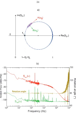
The frequency and dissipation noise are illustrated in Fig. 3.1 where contribution
100 101 102 103 104 105
Frequency (Hz)
Noise PSD (dBc/Hz)
Rotation angle (°)
–50 150
120
90
60 –60
–70
–80
–90
–100
Rotation angle
SAA(ν)
SBB(ν)
0 1
0
1–Qr/Qc
Re{S } 21
Im{S } 21
fr
*
A(ωg)
B(ωg) a)
b)
Figure 3.1: (a) The circular trajectory of the complex transmissionS21as a function of
corresponds to the amplifier noise floor which can be measured when the frequency
is tuned far from resonance. The frequency noise spectrum typically has a 1/ν shape below 10 Hz, a 1/ν0.5 shape above 10 Hz, and a rolloff that happens at the smaller
of the resonator bandwidth (fr/2Qr) or the intrinsic noise bandwidth ∆νn.
TLS noise is observed to scale with microwave readout power as P−1/2 and with
temperature as T−β with β = 1.5–2 [48, 42]. The power dependence is similar to the low-temperature TLS loss saturation effect in Eq. 3.2. Using these observations
Gao et al. developed a semiempirical model [36] for TLS noise in superconducting resonators. In this model the TLS fractional frequency (δfr/fr) noise power spectral density at high microwave readout powers is given by
STLS =κ(ν, ω, T) R
Vh| ~
E(~r)|3d3r
4RV |E(~~ r)|2d3r2
(3.9)
where κ(ν, ω, T) is defined as the noise spectral density coefficient and captures the ν−1/2 spectral shape and the dependence on microwave frequencyω and temperature.
The formula readily reproduces the power scaling as |E|−1 ∝ P−1/2, similar to what
is experimentally observed. This model has been confirmed experimentally through
observation of geometrical scaling of TLS noise with CPW center strip widthswhere it was observed [36] that noise scales as s−1.58. Based on strong evidence discussed
in Section 3.2 that TLS have a surface distribution, they numerically calculated the ~
E(~r) field for their CPW resonators assuming a surface distribution of TLS, and used
that result in their Eq. 3.9 to show that they get the same scaling as their experiment.
3.4
A microwave resonator design for reduced TLS
noise
Motivated by the implications of the semiempirical noise model discussed above, we
CPW feedline
Interdigitated capacitor
CPW inductor Submm-wave
Nb/SiO
microstrip line
Input Output
Al center strip Nb ground plane
wind gind wcap gcap
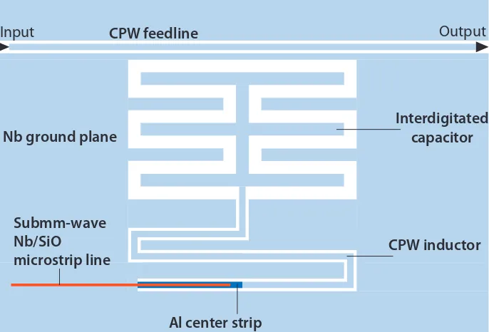
Figure 3.2: Schematic illustration of an interdigitated capacitor (IDC) resonator used in this work. wcap and scap are large to reduce TLS noise. For illustration purpose the dimensions are not to scale and the capacitor shown has only 5 fingers on each side. The actual devices have more fingers. The resonator is capacitively coupled to a CPW feedline. The resonator is mainly made from Nb on a Si substrate except for a∼1-mm-long aluminum-on-Si section. The CPW inductor is short-circuited at the Al end where the current is maximum. The mm/submm radiation can be brought to the resonator with a low-loss microstrip line where it is absorbed in the Al section.
TLS noise. Several different resonator geometries were designed in the beginning,
but in the end one design turned out to be most effective which is described in this chapter and for which measurements were taken.
A key prediction of the noise model in Eq. 3.9 is that the noise contributions from
individual TLS located on the resonator surface are weighted by |E~|3. This implies
that TLS located in high E-field areas are the main contributors to the noise. The
high E-field section of a resonator is its capacitive portion, and so by redesigning this portion one could potentially lower the noise. This can be done by widening the
electrode spacings in the capacitor which spreads the E-field distribution in a way that less electric field lines go though the surface TLS layer, effectively reducing the
We used this insight to develop a modified resonator geometry [35] in which the
capacitive section of a conventional λ/4 CPW resonator has been replaced by an interdigitated capacitor (IDC) structure with wide finger spacings (Fig. 3.2). The
inductive low E-field section was left unchanged as compared to our conventional CPW resonators. This makes it possible to directly compare our noise results with
regular CPW resonators. Furthermore, since we were planning to use these resonators as MKIDs for photon detection (initially with the MKIDcam instrument [50] and
later with the MUSIC instrument [17]; see Fig. 3.12), it was important to keep the inductive section narrow to maintain a high kinetic inductance fraction (α) needed
for maximum responsivity. The details of the actual fabricated devices are explained next.
3.4.1
Device details
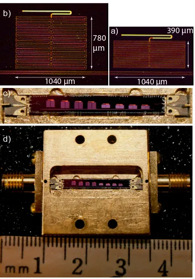
Figure 3.3 shows a picture of the fabricated resonators along with the device box.
There are 8 resonators on the chip corresponding to 2 different resonator geometries (4 of each geometry). Both geometries have IDCs but with different size.
The first geometry (Fig. 3.3 (a)) has an IDC made of 19 fingers on each side of the
vertical strip in the middle of the IDC. Finger width and spacing are wcap = 10 µm and gcap = 10 µm. The IDC is 1040 µm × 390 µm giving a capacitor area of 0.40 mm2 and a capacitance value ofC10−10≈2.0 pF. It is made from 200-nm-thick Nb on
a 450-µm-thick crystalline silicon substrate (with a thin native oxide layer expected
to be present due to air exposure) using a photoresist mask and an SF6 plasma etch.
The distance between the IDC and the feedline as well as the IDC width controls the
coupling of the resonator to the feedline Qc.
The narrow CPW meander acts as a CPW inductor that is short-circuited on
d)
c)
b)
a)
780
µm
1040 µm
390 µm
1040 µm
and MUSIC [17] instruments, and therefore it was designed to be as close to an
ac-tual photon sensor as possible which would help in identifying any unforeseen issues. Hence, part of the length of the inductor was made of a 1-mm-long CPW with the
center strip made from 60-nm-thick aluminum and the ground planes made from 200-nm-thick Nb. This section would act as the photon sensory part. The
millime-ter/submillimeter radiation collected using a separate antenna would then travel on a Nb/SiO2/Nb microstrip line reaching the beginning of the Al CPW section at the
shorted end. The microstrip line would then combine with the CPW turning into a Nb/SiO2/Al microstrip line. The radiation would then be absorbed in the aluminum
creating quasiparticles in the resonator (see Fig. 3.2). Since Al has a lower supercon-ducting energy gap (νAl
g ≈ 90 GHz) than Nb (νgN b ≈ 700 GHz), the Al section also keeps the quasiparticles trapped so they don’t escape. However, we did not include the microstrip line in the actual fabricated devices since the experiment was intended
to be done with the devices inside a dark cryostat for dark noise testing (no optical window to couple radiation from). In order to tune the resonance frequency and space
the four resonances∼50 MHz apart, a short extra length of pure Nb CPW inductor (lN b = 54–134 µm) is inserted between the Nb IDC and the Al CPW inductor.
The design of the second geometry (Fig. 3.3 (b))is the same as the first design
except for the IDC dimensions. It haswcap = 20µm andgcap= 20µm and is 1040µm
×780µm giving a capacitor area of 0.81 mm2 and a capacitance value ofC
20−20 ≈2.4
pF.
Fig. 3.3 (c) and (d) show the chip with the 8 resonators mounted inside a test
box. The box is made from oxygen-free high-purity copper that has been plated with a nonmagnetic gold layer to avoid exposing the magnetic-field-sensitive resonators
[51] to unwanted magnetic fields. The signal is brought in through the SMA coaxial connection on one side and read out from the other side. The center pin of the coaxial
connector is soldered to a microstrip line on a duroid circuit board. The microstrip line transitions to a CPW on this board and is brought to the chip using wirebonds
Before describing the measurements on this device we will mention a few important
design considerations that are important for IDC resonators.
3.4.2
Some design considerations
In order to reduce TLS noise as much as possible, the capacitor area and electrode spacings (wcap and scap) have to be made as large as possible. However, the IDC can quickly get too big resulting in several issues. One is that the IDC could act as a distributed element with propagating modes rather than a lumped capacitor.
This would result in nonzero microwave currents in the capacitor that can introduce parasitic inductance reducing the effective capacitance and also reduce the kinetic
inductance fraction in case the resonator is being used as an MKID. This can happen if the size is larger than ∼λ/20 where λ is the wavelength of the propagating mode.
For a 5 GHz resonator on a silicon substrate ∼ λ/20 = 1.2 mm assuming a CPW propagating mode. The IDCs in our resonators are close to the limit of
lumped-element performance. We simulated the capacitors in Sonnet [52] and confirmed that they are close to being lumped-element, although some amount of currents were
produced in the capacitors.
Another concern is microwave radiation into the substrate from the capacitor which could reduce the internal quality factor of the resonator. This can happen in
certain types of large IDC or CPW structures if not properly designed. For example, from a TLS noise point of view, one could use a “fat” CPW resonator where the center
strip width and gaps are increased to reduce noise. However, such a structure can ra-diate into space significantly reducing the quality factor [13]. To minimize microwave
radiation it is important to design the structure so that opposite polarity conductors are always close to each other canceling the radiation from opposite polarity currents.
This is also important for large IDC structures and in fact became an issue in our initial design where we had used a slightly different IDC structure. The lost power
Sonnet [52] by looking at 1− |S11|2 for a one-port circuit element like an IDC, or by
running a two-port simulation for the whole resonator with a feedline and looking at 1− |S11|2− |S21|2, where S11 and S21 are the microwave scattering parameters.
Another important issue for an array of MKID resonators on a chip is the limited space availability for each resonator. Interdigitated capacitors with wide finger
spac-ings can take a significant amount of area on chip and are not necessarily the best option for use in tightly packed MKID arrays. For example, parallel-plate capacitor
structures on silicon-on-insulator substrates [53] can take much less area for the same amount of capacitance and could provide an alternate solution for s