Volume 2006, Article ID 79595, Pages1–9 DOI 10.1155/ASP/2006/79595
Highly Flexible Multimode Digital Signal Processing Systems
Using Adaptable Components and Controllers
Vinu Vijay Kumar and John Lach
Charles L. Brown Department of Electrical and Computer Engineering, University of Virginia, Charlottesville, VA 22904, USA
Received 1 October 2004; Revised 21 March 2005; Accepted 25 May 2005
Multimode systems have emerged as an area- and power-efficient platform for implementing multiple timewise mutually ex-clusive digital signal processing (DSP) applications in a single hardware space. This paper presents a design methodology for integrating flexible components and controllers into primarily fixed logic multimode DSP systems, thereby increasing their overall efficiency and implementation capabilities. The components are built using a technique called small-scale reconfigurability (SSR) that provides the necessary flexibility for both intermode and intramode reconfigurabilities, without the penalties associated with general-purpose reconfigurable logic. Using this methodology, area and power consumption are reduced beyond what is pro-vided by current multimode systems, without sacrificing performance. The results show an average of 7% reduction in datapath component area, 26% reduction in register area, 36% reduction in interconnect MUX cost, and 68% reduction in the number of controller signals, with an average 38% increase in component utilization for a set of benchmark 32-bit DSP applications.
Copyright © 2006 Hindawi Publishing Corporation. All rights reserved.
1. INTRODUCTION
The burgeoning demand for high performance DSP sys-tems has spurred widespread research on efficient platforms for implementing arithmetic intensive applications charac-teristic of such systems. Based on these applications’ high throughput requirements, fixed logic application-specific in-tegrated circuits (ASICs) are normally the platform of choice. However, their lack of flexibility is disadvantageous in today’s world of disparate and rapidly evolving standards and appli-cations, which require the execution of a variety of DSP tasks. In the absence of flexibility, direct hardware implementation of all of the tasks is the only option and can be prohibitively expensive—even in this “transistors for free” era. This has led to the search for new methods for adding flexibility to other-wise fixed logic DSP circuits, without having to pay the large performance, area, and power penalties associated with field programmable gate arrays (FPGAs), DSP processors, or even application-specific instruction processors (ASIPs).
An emerging platform that has been proposed to address the flexibility issue in ASICs for DSP is “multimode” systems [1,2]. Tasks that are timewise mutually exclusive are syn-thesized to the same hardware area, allowing the tasks to be separated temporally rather than spatially. When a particu-lar task must be executed, the system switches to the appro-priate hardware configuration “mode.” Such a design plat-form can prove useful for many DSP systems. For example,
a system jointly implementing two different standards (e.g., CDMA/GSM formats in a cell phone, different region DVD formats in a Universal DVD player, etc.), where only one mode needs to be active at any given time, can benefit from a multimode implementation.
However, current multimode systems are severely con-strained in their capabilities and efficiency due to their lim-ited reconfigurability. Reconfiguration between modes is ac-complished by changing only the dataflow between compo-nents; the datapath components themselves do not change. The individual controllers for each mode are composed to-gether into a single controller that also does not change be-tween modes. Hence, such a system is inefficient and not very powerful, with only the interconnections changing between modes.
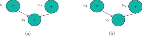
v1 v2
v3
∗ ∗
+
(a)
v4 v5
v6
∗ +
+
(b)
Figure1: Sample DFGs.
used to provide the hardware flexibility, the technique pre-sented here uses small-scale reconfigurability (SSR) [3,4]. SSR provides hardware flexibility without the area, delay, power, and reconfiguration time penalties associated with general-purpose reconfigurable fabric.
1.1. Illustrative example
Consider the two dataflow graphs (DFGs) inFigure 1, each representing a different mode of a DSP system. The datap-ath and controller designs must be capable of implementing either mode.
1.1.1. Datapath design
Assuming the system is not pipelined and specifications dic-tate that modes have minimum latency, DFG 1a (Figure 1(a)) would require two multipliers (MULTs) and one adder (ADD), and DFG 1b (Figure 1(b)) would require one MULT and one ADD. If both tasks were implemented spatially sep-arately, the total number of arithmetic components would be three MULTs and two ADDs.
However, if the tasks are timewise mutually exclusive, they may be implemented using existing multimode tech-niques in which components may be shared by both tasks, but must remain fixed. Such an implementation would re-quire only two MULTs and one ADD, and the proper mode would be invoked based on the task to be implemented. While the tasks share datapath components, they require sep-arate controllers. In addition, interconnect complexity is also high, as component interconnections have to support the dataflow in both product instances. For example, the adder component producing the overall output (mapped to nodes
v3orv6) gets its inputs either from the two multipliers (for
DFG 1a) or from a multiplier and itself (for DFG 1b), requir-ing a MUX to be added at the inputs that was unnecessary in the separate single-mode implementations.
Now consider a flexible arithmetic component (FAC) ca-pable of performing both addition and multiplication that is as fast as a multiplier but is smaller than the combined areas of an adder and multiplier (although larger than each indi-vidually). For example, the “morphable multiplier” uses the adder chains within the multiplier to perform addition with minimal area and no delay penalties [5]. The flexibility of a FAC is such that not only can it be a multiplier in one mode and an adder in another (intermode reconfiguration), but it could also be an adder and a multiplier in different control steps (c-steps) within the same mode (intramode reconfigu-ration).
Using FACs and intramode reconfiguration, DFG 1a can be implemented with one MULT and one FAC, with the FAC switching between a MULT (to executev2 in c-step 1)
and an ADD (to execute v3 in c-step 2). If DFG 1b were
synthesized independently, the technique would allocate one MULT and one ADD. But given that the two DFGs are to be implemented in the same physical multimode space, they can be synthesized together, resulting in one MULT and one FAC. Given the assumption that one FAC is smaller than the combined area of an adder and a multiplier, area sav-ings are achieved over existing limited reconfigurable mul-timode synthesis techniques. Component utilization is also increased, reducing wasted power consumption. Note that if only intermode reconfiguration is utilized (with the FAC functionality being fixed within a mode through all c-steps), the component allocation would be an ADD, a MULT, and a FAC, which still provides an improvement over the nonmul-timode implementation.
This technique also inherently leverages any inter- and intra-DFG isomorphism. Using efficient binding of flexible components to nodes, the need for MUXes in the intercon-nection network is minimized without the need for any iso-morphic subgraph identification and matching on the nodes in the DFG. Consider that nodesv1andv4inFigure 1use the
MULT component and nodesv2,v3,v5, andv6use the FAC,
so the component interconnects will not change from one mode to the other. Without the FAC,v2andv5would be
ex-ecuted on a MULT and ADD, respectively. Both operations’ results would be input to the ADD, requiring a 2 : 1 MUX for the ADD and MULT to write to the same result register or for the ADD to read from different source registers for the different modes. For large system bit widths, MUXes become very expensive. The technique presented here minimizes the need for such MUXes (and control signals for the MUXes, which must be generated individually for each mode), while avoiding computationally intensive subgraph isomorphism identification algorithms [6].
1.1.2. Controller design
Conventional multimode or domain-specific customization approaches, where fixed datapath components are shared be-tween tasks, require separate controllers, with the individual controllers typically MUXed at their outputs to form a com-posite controller. However, the comcom-posite controller in such designs often becomes complex enough to require a pro-grammable microcode-based implementation, which is less area- and power-efficient and has lower performance than hardwired controllers.
SSR-based adaptable controllers can reduce these ineffi -ciencies. Consider now a composite controller for the multi-mode system shown inFigure 1. Assume that the individual instance controllers have only minor differences; say, for ex-ample, one of their output functions is represented by f1in
one and f2in the other. Assume f1and f2are defined as
fol-lows: f1=a+b+ce+de; f2=ac+ad+bc+bd+e. For a
for the specific mode could be performed with an output MUX. Using only 2-input fixed logic gates from a standard cell library such as the Lsi10k library, the total circuit cost for such an implementation is 19 inverter-equivalent gates.
The SSR-designed flexible controller provides the same flexibility more efficiently. f1 and f2are jointly synthesized
as a multi-output function, thus maximizing logic sharing between the functions and automatically obtaining the min-imum implementation difference between them. The shared logic (in this case, the common subexpressionsX=a+band
Y =c+d) is then implemented in fixed logic, while the
differ-ences are implemented in configurable logic. In our example, the functions f1andf2are rewritten as f1=X+e∗Yandf2=
X∗Y+e, and jointly implemented using programmable inter-connect for a total circuit cost of 12 inverter-equivalent gates. An algorithmic framework for integrating flexible datap-ath and control components into multimode systems is pre-sented in this paper. Conventional high-level synthesis tools do not take advantage of the range of flexibility provided by these components. For example, module allocation tech-niques for multifunction ALUs (e.g., using operation clus-tering, etc.) are not optimized for application-specific, lim-ited flexibility addition. Other approaches for incorporating ALUs, in which allocation precedes synthesis, are ineffective for multimode systems since inter-DFG dependencies are not effectively extracted for optimum allocation. In the following sections, new algorithms and extensions to conventional al-gorithms are proposed for datapath synthesis, allocation, and binding, and for automatic control path synthesis for multi-mode DSP systems with flexible components and controllers.
2. BACKGROUND AND RELATED WORK
In order to leverage the increasing relative performance, area, and power benefits of hardware versus software, there is a trend towards implementing in hardware many algorithms and applications that had previously been done primarily in software. This is particularly evident with the advent of embedded syston-a-chip (SOC) designs, in which em-bedded processors and application-specific circuitry share the processing load based on a designer-defined partition. For applications requiring several disparate performance-sensitive tasks, this often results in low resource utilization, a metric for hardware efficiency.
One approach that has been suggested to address the low resource utilization issue, as well as to enable more power-ful hardware implementations of DSP systems, is to jointly synthesize different applications to build a unified datapath. By using separate controllers, the datapath may be animated to implement the various applications. This method was first explored in [2] as “multifunctional processing units.” The work provided heuristic local search algorithms for the joint allocation of components so as to minimize intercon-nect. Designing application-specific programmable proces-sors (ASPPs) by bundling similar applications and jointly synthesizing them has also been investigated [7]. Flexible datapaths have been proposed for fault tolerance purposes,
with various configurations available to recover from com-ponents failures [8]. Most recently, a “spatially chained trans-formation” was introduced to enable dataflow graphs of dif-ferent applications to be chained together for joint compo-nent allocation and binding [1]. The essential element in all of these efforts is that timewise mutually exclusive applica-tions can reside in different configuraapplica-tions in the same phys-ical area of a “multimode” system.
Domain-specific customization is a related approach for application-specific flexibility in reconfigurable systems [6, 9]. This approach involves creating a custom reconfigurable architecture to specifically implement a set of circuits from a given domain and be completely flexible within that do-main. This is, in a sense, a mirror image of our approach. While ours is aimed at inserting small amounts of reconfig-urability into primarily fixed logic circuits, domain-specific customization inserts fixed logic into circuits with primarily reconfigurable fabric. The synthesis techniques developed for such systems, therefore, address a different set of issues (e.g., template generation, isomorphic subgraph identification and matching, etc.) that is relevant to domain-specific customiza-tion. It is difficult to adapt these techniques to address is-sues specific to our problem, such as runtime reconfigurabil-ity within isomorphic subgraphs. The technique presented in this paper addresses such issues.
While hybrid FPGAs and reconfigurable cores provide hardware flexibility, their coarse integration of fixed logic and reconfigurable fabric result in significant area, perfor-mance, and power penalties. Techniques have therefore been explored to add flexibility to individual hardware compo-nents without the penalties associated with general-purpose reconfigurable arrays. By reusing adder chains within a mul-tiplier, an area-efficient “morphable” multifunction compo-nent capable of both addition and multiplication was de-scribed in [5]. Such a unit is useful in DSP systems domi-nated by multiply-accumulate (MAC) chains. Another flexi-ble component capaflexi-ble of both single-precision and douflexi-ble- double-precision floating point multiplication was described in [10]. Synthesis techniques that integrate flexible components into primarily fixed logic systems are detailed in [3]. That work augmented traditional force-directed list scheduling (FDLS) [11] for component scheduling and allocation using a hybrid library of fixed and reconfigurable arithmetic components, providing significant area savings for single-mode systems. The work presented here provides hybrid library synthesis techniques for multimode systems, yielding even greater sav-ings.
3. EFFICIENT FLEXIBLE HARDWARE
The SSR design technique minimizes these penalties by inserting into a primarily fixed logic design only the flexibil-ity that is required for a specific application. Reconfigurable logic and interconnect (e.g., SRAM-based LUTs, MUXes, SRAM-gated pass transistors, etc.) are finely integrated with fixed logic at a gate-level granularity. While some recent technologies contain both fixed and reconfigurable logic on the same chip, they are coarsely integrated. For example, some hybrid FPGAs contain a fixed logic core surrounded by general-purpose reconfigurable fabric. Domain-specific cus-tomization [6,9], discussed inSection 2, provides another example. SSR allows for finer integration and application-specific implementation, providing the necessary flexibility with ASIC-like efficiency. In addition, the reconfiguration time is significantly shorter, as there is less to reconfigure. The tradeoff is the design effort and fabrication costs as-sociated with all ASICs, but high-volume applications off-set these costs, and many applications require ASIC perfor-mance.
The SSR design methodology can be applied to a range of designs and applications. The remainder of this section focuses on the use of SSR for designing FACs and adaptable finite state machines (FSMs), which enable efficient datapath and control flexibility.
3.1. Flexible arithmetic components
When designing a FAC, the similarities between the desired operations can be implemented in fixed logic, and reconfig-urable logic and interconnect must be used to implement the differences. Therefore, the first step in designing a FAC with SSR is to determine the minimum distance between the oper-ations to be implemented, thereby minimizing the need for reconfigurable hardware (and its associated penalties). Cer-tain operations have inherently greater similarities than oth-ers, making them more conducive to SSR implementation. For example, adders and multipliers have similar substruc-tures, resulting in an especially efficient flexible implementa-tion.
Other DSP operation combinations may also be consid-ered for FAC implementation: a wide bit width operation could be integrated with multiple operations of narrower width; several low-precision operations could be embedded within a high-precision operation [10]; a rarely used opera-tion could be integrated within a high use operaopera-tion (increas-ing hardware usage); and so on. In addition, reconfigurable rounding modes may be added so that the binary point of the output can be moved based on the inputs and desired round-ing. This would address the rounding inaccuracy and scaling problems that plague conventional fixed-point components used in hardware signal processing. As stated inSection 1.1, for a FAC to provide area savings, its area must be smaller than the combined area of all of the operations implemented individually.
FACs built using SSR avoid the large performance, area, and power penalties associated with FPGAs and DSP pro-cessors. For example, we have presented a flexible com-ponent capable of executing a 4-bit fixed-point addition,
subtraction, multiplication, or comparison [3]. The areas of the various components normalized in terms of the com-parator (which is the smallest of the fixed components at 52 inverter-equivalent gates) were obtained as Comparator:
X, Adder/Subtractor: 1.44X, Multiplier: 4.5X, Limited Flexi-ble Unit (LFU; Adder/Subtractor and Multiplier): 4.81X, and Full Flexible Unit (FFU; Comparator, Adder/Subtractor, and Multiplier): 5.31X. The flexible units were therefore of very reasonable size compared to the fixed logic units. To com-pare these inverter-equivalent gate counts to an FPGA im-plementation, the largest fixed component (i.e., the multi-plier) was considered. The 4-bit multiplier implemented on an FPGA with 4-input LUTs required 82 LUTs (using the Xil-inx ISE software package). At an approximate area cost of 80 inverter-equivalent gates for each LUT, this is equivalent to 6560 inverters or 126.15X. This does not include the in-terconnect network, which consumes the majority of recon-figurable fabric area. Reconfiguring the flexible components is also efficient since it just involves changing the configu-ration bits for a single 4-input look-up table and select sig-nals for internal MUXes as opposed to reconfiguring large ar-eas of an FPGA. Small-scale reconfigurability clearly provides hardware flexibility with significantly less area than general-purpose FPGAs. Since FPGAs are, in general, more efficient than DSP processors when customized for a particular appli-cation, SSR provides greater benefits overall.
While SSR provides area savings, delay penalties must also be considered, as the length of a c-step may increase with flexible components. For the 4-bit components in [3], the relative path delays of the components were Compara-tor: Y, Adder/SubtracCompara-tor: 2Y, Multiplier: 3.67Y, LFU: 4.67Y, and FFU: 5Y, with the approximation that all combinational gates have equal delays. Therefore, assuming the length of the c-step was defined by the multiplier delay, the use of an LFU or FFU will increase the c-step length by 27% and 36%, re-spectively. These increases must be traded offwith the area savings provided by hybrid library scheduling and allocation. In addition, these delays are significantly less than those of an FPGA, revealing the delay benefit of SSR.
It must be noted that the specific multiplier chosen for comparison is that with the shortest critical path. For other multiplier structures, the percentage delay increase would be smaller. For example, the results in this paper use an aug-mentation of the “morphable multiplier” [5], which is ca-pable of implementing both multiplication and addition (in fact, it can perform two data-independent additions in paral-lel) with the same delay as a fixed logic multiplier. Given the regularity with which MAC operations occur in DSP algo-rithms, this FAC provides significant benefits for multimode DSP systems. This component and the augmentations per-formed are discussed inSection 5.
3.2. Flexible controllers
choice given their smaller area and higher performance. However, when one considers designing a single flexible con-troller capable of being adapted for each mode, microcode has been the traditional option, as different microinstruc-tions can be loaded for each mode. But as with FPGAs, the area, performance, and power costs of microcoded con-trollers make them significantly less efficient that hardwired FSMs.
SSR can again be used to find the minimum distance between the various mode controllers to implement an ef-ficient flexible hardwired FSM. Consider that an FSM can be defined as a six-tupleS,I,O,S0,δ,λ, whereSis the set of
states, I is the input set,Ois the output set, S0 is the
ini-tial state,δis the state transition function set, andλis the output function set. For an FSM to be made flexible, theδ
andλ functions can be implemented using SSR such that they can be configured to implement the various mode con-trollers (including the control signals setting the FAC func-tionalities), and the cardinality ofSis defined by the maxi-mumScardinality of the individual mode controllers. Such an implementation is likely to be significantly more efficient than either separate hardware controllers or programmable microcode.
The adaptable FSM is optimally implemented as follows. The set of state transition functions defined byδ is fed to a logic synthesis tool and jointly synthesized as a multiple-output function circuit with logic sharing between the func-tions. The shared logic in the final synthesized circuit is the logic common to all of the functions and is implemented in fixed logic. The logic specific to each function is imple-mented in reconfigurable logic (using LUTs and/or MUXes) and changes between contexts. The process is repeated for the
λset.
This process is efficient as long as the intermode func-tions differ only slightly from each other. The multimode system synthesis techniques detailed in the following section help to minimize these differences, ensuring an efficient im-plementation. It should be noted that the number of config-uration control bits is limited due to the small scale nature of SSR. Therefore, the extra logic needed for generating these bits in the flexible FSMs is small compared to the savings ob-tained in simplifying the steering logic for the interconnect MUXes.
4. MULTIMODE DSP SYSTEM SYNTHESIS
While the SSR design methodology helps to enable efficient flexible hardware, a multimode DSP system’s efficiency is ul-timately driven by high-level synthesis, which ensures the flexibility is used efficiently. General multimode synthesis techniques are emerging, but this section presents the first multimode DSP system synthesis technique that incorpo-rates FACs and adaptable FSMs. In fact, it is noted by the designers of the morphable multiplier that no synthesis tech-niques exist that make use of such components [5].
The steps inFigure 2detail the synthesis methodology and are explained via the subsequent example.
(1) input DFGs and system and DFG-specific constraints; (2) identify the set of potential arithmetic components; (3) traverse DFGs for critical paths;
(4) for each DFG (in order of increasing slack) HFDLS (DFG); HAL (DFG);
(5) c-step matching (scheduled DFGs);
(6) for each DFG (in order of decreasing resource usage) bind (DFG);
(7) design controller.
Figure2: Multimode system synthesis methodology.
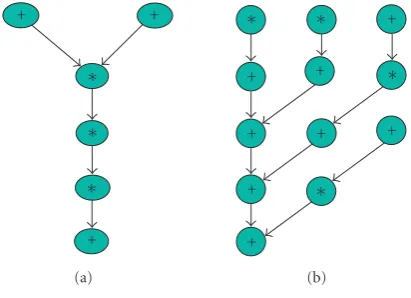
+ +
∗
∗
∗
+
(a)
∗
+
+
+
+
∗
+
+
∗
+
∗
+
(b)
Figure3: Sample DFGs.
In step 1, the inputs to the system are the individual DFGs, representing the signal processing modes and an op-tional overall delay and/or resource constraint on the whole system. Parameters associated with each DFG, such as the precision, data width, and maximum tolerable latency (or optionally, the resource constraint), are also input to the sys-tem. (The results inSection 5are for deriving the minimum resource allocation under latency requirements. Future work will address other scenarios.)
The DFGs are then traversed in step 3 to find the critical paths based on data dependencies and the operation latency assumptions. Counting additions as one c-step and multi-plies as two, the longest paths on DFG 3a and DFG 3b are eight and six steps, respectively. Therefore, to meet the la-tency constraints of each DFG, there is no c-step slack for DFG 3a and one c-step for DFG 3b. This determines the DFG scheduling order, with the DFG with the least slack scheduled first.
Therefore, DFG 3a is scheduled first in step 4 using hy-brid force-directed list scheduling (HFDLS) and hyhy-brid allo-cation (HAL) [3]. Unlike the conventional FDLS algorithm that lowers the concurrency of same-type operations per c-step, the HFDLS algorithm uses a modified force calculation such that an overall balance in the number of operations per c-step is achieved. The HFDLS algorithm has the same worst case computational complexity as FDLS:O(n2), wherenis
the number of nodes to be scheduled in each DFG. After scheduling, general multifunction ALU allocation algorithms can be used by considering the flexible component as a kind of limited ALU. However, the bulk of the work in creating an optimum schedule requiring the minimum number of flex-ible components is done by HFDLS, and a simple allocation algorithm, such as HAL, is sufficient to allocate components on these scheduled graphs. HAL uses principles from set the-ory to produce an exact minimum module allocation set. The algorithm has a computational complexity ofO(m), wherem
is the number of adder and multiplier nodes to be allocated. Further details on both HFDLS and HAL can be found in [3]. Given that DFG 3a has no slack, it must be scheduled in the fewest number of c-steps. The resulting scheduled DFG is shown inFigure 4. From this schedule, it is clear that two ADDs and one MULT would be necessary if only fixed com-ponents were available. However, this DFG can be imple-mented with a single FAC. Given the relative size of the var-ious components, this represents a large reduction in area, even within a single mode. (This echoes the results in [3], which focus on FACs in single-mode systems.)
Once the first DFG is scheduled, the other DFGs are each scheduled (in the order of increasing slack) so that they meet their individual latency requirements. For each DFG, an at-tempt is made to meet the required latency without more re-sources than are currently allocated. When the resource allo-cation must be increased to meet a latency requirement, the global resource allocation is updated. While an increase in the allocation set may enable already scheduled DFGs to re-duce latency by rescheduling, the algorithm does not do so, as the DFG latency requirements have already been met. In-stead, this resource slack is exploited during binding, as dis-cussed below. When all of the DFGs are scheduled, the fi-nal resource allocation set, including both fixed and flexible components, is known.
When DFG 3b is scheduled using this approach, it is ob-vious that it cannot be scheduled with only one FAC. There-fore, the number of resources must be increased. The mini-mum resource set to schedule DFG 3b, while meeting its la-tency requirement, is two FACs, as opposed to 2 ADDs and 2 MULTs if FACs were not available. The resulting scheduled
+ +
∗
∗
∗
+
Figure4: Scheduled DFG for DFG 3a.
∗
∗
∗
∗
+ +
+
+
+
+ +
+
Figure5: Scheduled DFG for DFG 3b.
DFG is shown inFigure 5. (Note that the schedule would be different if only fixed components were available, as HFDLS often produces different schedules than traditional FDLS.) Even though we increased the component allocation, we do not reschedule DFG 3a. (Note that in this case the schedule would not change anyway.)
If the DFGs have different numbers of c-steps, step 5 matches c-steps across the DFGs. The goal is to maximize same-control-step component usage, thus minimizing the functional differences between the various mode controllers for an efficient adaptable FSM design. This matching is done using maximal weighted matching, which can be solved in polynomial time [11]. The weight assigned to each control-step-connecting edge in the matching graph is the number of resources common to the connected c-steps.
Step 6 binds operations to components, starting with the DFG that last set the resource allocation, as it is typi-cally the mode with the highest component utilization. Max-imal weighted matching is used to minimize interconnect, MUXes, and registers [13]. An important change to tradi-tional binding is that the graph is constructed with compat-ibility edges drawn from operation nodes not only to com-ponents of that type but also to FACs, albeit with a smaller “component match” weight factor.
In binding the other DFGs, an effort is made to minimize interconnect, MUX, and register overhead above that set by the base DFG as well as to simplify the subsequent controller design. The key benefit provided by FACs is that subgraphs within a DFG with different operations are actually isomor-phic in both nodes and edges if the disparate operations can be bound to the same FAC. Therefore, the binding algorithm is likely to find a larger number of subgraphs and individual nodes that share inputs/outputs. These benefits are further enhanced by the resource slack in the DFGs that were not rescheduled after additional resources were allocated.
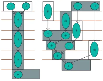
The binding result for DFGs 3a and 3b are shown in Figure 6. The different block shadings represent the two FACs. Note that the darkly shaded component always out-puts to itself, except for c-step 1 in DFG 3b, and the lightly shaded component always feeds the same input port of the other component. This matching helps minimize the inter-connect, MUXes, and registers.
The final step is controller design. As discussed inSection 3.2, SSR and multiple output logic synthesis enable the con-trollers for all of the modes to be implemented in the same physical space, with their similarities implemented in fixed logic and interconnect and their differences in reconfigurable logic. The outputs of the FSM include the control signals for the MUXes, register enables, and FAC settings.
None of these steps in this process are more computa-tionally complex than what is currently done for multimode system synthesis, but as the results show in the following sec-tion, the area and power savings can be significant.
5. RESULTS
The methodology presented in this paper has been evalu-ated by synthesizing multimode DSP systems with runtime reconfiguration. The base DFGs used are well-known DSP instances from the high-level synthesis literature. The param-eters of these DFGs, in terms of number of nodes, minimum latency, and so forth, span a wide range and are representa-tive of the kind of DFGs that occur in multimode systems. ELLIP is a fifth-order elliptic digital filter with 33 operations and minimum latency of 13 c-steps [12], EDGE is an edge detector with 241 operations and minimum latency of 121 c-steps [13], ARFILT is an autoregressive filter with 28 op-erations and minimum latency of 8 c-steps [14], FDCT is a fast discrete Fourier transform instance with 42 operations and minimum latency of 6 c-steps [15], and FIRFILT is a 16-point FIR filter with 23 operations and minimum latency of 9 c-steps [16].
The datapath is assumed to be 32-bit wide in all of the example systems. The component library consists of 32-bit
+ +
∗
∗
∗
+
∗
+
+
+
+ +
+
∗
∗
∗
+ +
Figure6: Bounded DFGs.
fixed logic adders, multipliers, and FACs capable of both ad-dition and multiplication (including two data-independent ADDs in one c-step). Other FACs (including those not specific to DSP applications) will be considered as part of future work. As discussed in Section 3.1, the FAC is based on the morphable multiplier [5]. The component areas in terms of the number of constituent transistors are as follows: ADD = 1306, MULT = 6150, FAC = 6860. The multi-plier and multiply-configured FAC have latencies of two c-steps. Pipelined versions of these components can be built at a cost of approximately 1000 additional transistors each, which would be necessary if the required maximum latency was less than what non-pipelined components allowed. Re-configuring this component simply involves sending the ap-propriate select signal to internal MUXes and is virtually in-stantaneous.
Table1: Component allocations and utilizations.
MM system SMFixed MMFixed MMFlex Improvement (%)
+ * Area Util. (%) + * Area Util. (% ) + * FAC Area Util. (%) Area Util. (%) AR, FDCT, FIR 7 14 95 242 17.9% 4 8 54 424 37.5% 1 6 2 51 926 44.7% 4.59% 19.2% ELLIP, FIR 5 4 31 130 29.1% 3 2 16 218 52.3% 1 0 2 15 026 73.2% 7.35% 40.0% ARFILT, FDCT 6 12 81 636 29.7% 4 8 54 424 44.6% 0 6 2 50 620 56.2% 6.99% 26.0% FIR, EDGE 4 4 29 824 36.1% 3 2 16 218 57.8% 1 0 2 15 026 90.1% 7.35% 55.9% ELLIP, EDGE 4 4 29 824 33.6% 3 2 16 218 53.7% 1 0 2 15 026 81.5% 7.35% 51.8%
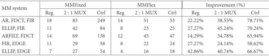
Table2: Registers, MUXes, and control signals.
MM system MMFixed MMFlex Improvement (%)
Reg 2 : 1 MUX Ctrl Reg 2 : 1 MUX Ctrl Reg 2 : 1 MUX Ctrl AR, FDCT, FIR 18 83 249 14 51 53 22.22% 38.55% 78.71%
ELLIP, FIR 11 42 84 8 23 25 27.27% 45.24% 70.24%
ARFILT, FDCT 14 69 138 12 45 47 14.29% 34.78% 65.94%
FIR, EDGE 11 29 58 8 22 24 27.27% 24.14% 58.62%
ELLIP, EDGE 7 27 54 4 16 18 42.86% 40.74% 66.67%
Table3: Controller logic areas.
MM system MMFixed MMFlex Improvement Controller area Controller area (%) AR, FDCT, FIR 1094 709 35.19%
ELLIP, FIR 416 263 36.78%
AR, FDCT 506 354 30.04%
FIR, EDGE 294 133 54.76%
ELLIP, EDGE 266 202 24.06%
The increased resource utilization also results in less wasted power consumption. For all three implementations, turning off components that are completely unused in a mode will help reduce power, but the overhead of turn-ing components on/offprevents intramode component shut down.
While these datapath area savings are significant,Table 2 shows that even larger savings are provided in terms of regis-ters, MUXes, and control signals. The register and 2 : 1 MUX reductions, due primarily to the binding process, are espe-cially valuable, as the 32-bit wide datapath makes these com-ponents large. The∼70% reduction in the number of control lines (ctrl) to the datapath from the controller, which among other things helps to simplify placement and routing, is ob-tained as a result of both the binding process as well as the use of adaptable controllers.
The controller logic area is also reduced, as shown in Table 3. Since separate controllers need not be built, the logic is greatly simplified. The area numbers shown are in terms of inverter-equivalent gates and are only for the combina-tional portion of the controller that implements the output functions, including any LUTs in the case of the adaptable
controller. The flip-flops and other memory elements in both the fixed controller and the adaptable controller are the same and are hence not included in the area results.
6. CONCLUSIONS
This paper presented an approach for synthesizing multi-mode DSP systems with a hybrid library of fixed and flex-ible arithmetic components and adaptable controllers. The implementation capabilities and efficiency of the multimode system platform is greatly increased by the extra hardware flexibility provided by small-scale reconfigurability, without the large area, performance, and power penalties associated with general-purpose reconfigurable fabric. The intramode reconfiguration and the scheduling, allocating, and binding flexibility provided by the FACs result in significant datapath and control area savings and wasted power consumption re-duction over existing multimode DSP system synthesis tech-niques.
7. ACKNOWLEDGMENTS
This work is supported in part by the National Science Foundation under Grant numbers CCR-0105626 and EHS-0410526 and by the Woodrow W. Everett, Jr. SCEEE Develop-ment Fund in cooperation with the Southeastern Association of Electrical Engineering Department Heads.
REFERENCES
[2] A. van der Werf, M. J. H. Peek, E. H. L. Aarts, J. L. Van Meerbergen, P. E. R. Lippens, and W. F. J. Verhaegh, “Area optimization of multi-functional processing units,” in Pro-ceedings of IEEE/ACM International Conference on Computer-Aided Design (ICCAD ’92), pp. 292–299, Santa Clara, Calif, USA, November 1992.
[3] V. Vijay Kumar and J. Lach, “Designing, scheduling, and allo-cating flexible arithmetic components,” inProceedings of 13th International Conference on Field Programmable Logic and Ap-plications (FPL ’03), pp. 1166–1169, Lisbon, Portugal, Septem-ber 2003.
[4] V. Vijay Kumar and J. Lach, “Heterogeneous redundancy for fault and defect tolerance with complexity independent area overhead,” inProceedings of 18th IEEE International Sympo-sium on Defect and Fault-Tolerance in VLSI Systems (DFT ’03), pp. 571–578, Boston, Mass, USA, November 2003.
[5] S. M. S. A. Chiricescu, M. A. Schuette, R. Glinton, and H. Schmit, “Morphable multipliers,” inProceedings of 12th Inter-national Conference on Field Programmable Logic and Applica-tions (FLP ’02), pp. 647–656, Montpellier, France, September 2002.
[6] K. Compton and S. Hauck, “Flexibility measurement of domain-specific reconfigurable hardware,” inProceedings of ACM/SIGDA 12th International Symposium on Field Pro-grammable Gate Arrays (FPGA ’04), pp. 155–161, Monterey, Calif, USA, February 2004.
[7] K. Kim, R. Karri, and M. Potkonjak, “Synthesis of appli-cation specific programmable processors,” in Proceedings of ACM/IEEE 34th Design Automation Conference (DAC ’97), pp. 353–358, Anaheim, Calif, USA, June 1997.
[8] L. M. Guerra, M. Potkonjak, and J. M. Rabaey, “Behavioral-level synthesis of heterogeneous BISR reconfigurable ASIC’s,”
IEEE Transactions on Very Large Scale Integration (VLSI) Sys-tems, vol. 6, no. 1, pp. 158–167, 1998.
[9] E. Bozorgzadeh, S. O. Memik, R. Kastner, and M. Sarrafzadeh, “Pattern selection: customized block allocation for domain-specific programmable systems,” in Proceedings of Interna-tional Conference on Engineering of Reconfigurable Systems and Algorithms (ERSA ’02), Las Vegas, Nev, USA, June 2002. [10] G. Even, S. M. Mueller, and P.-M. Seidel, “A dual mode IEEE
multiplier,” inProceedings of 2nd Annual IEEE International Conference on Innovative Systems in Silicon (ISIS ’97), pp. 282– 289, Austin, Tex, USA, October 1997.
[11] P. G. Paulin and J. P. Knight, “Force-directed scheduling for the behavioral synthesis of ASIC’s,” IEEE Transactions on Computer-Aided design of Integrated Circuits and Systems, vol. 8, no. 6, pp. 661–679, 1989.
[12] S. Park and K. Choi, “Performance-driven high-level synthesis with bit-level chaining and clock selection,”IEEE Transactions on Computer-Aided Design of Integrated Circuits and Systems, vol. 20, no. 2, pp. 199–212, 2001.
[13] R. M. Haralick and L. G. Shapiro,Computer and Robot Vision, Addison-Wesley, Reading, Mass, USA, 1992.
[14] K. H¨ogstedt and A. Orailoglu, “Integrating binding con-straints in the synthesis of area-efficient self-recovering mi-croarchitectures,” inProceedings of IEEE International Confer-ence on Computer Design: VLSI in Computers and Processors (ICCD ’94), pp. 331–334, Cambridge, Mass, USA, October 1994.
[15] D. J. Mallon and P. B. Denyer, “A new approach to pipeline optimisation,” inProceedings of European Design Automation Conference (EDAC ’90), pp. 83–88, Glasgow, Scotland, UK, March 1990.
[16] R. Karri and A. Orailoglu, “High-level synthesis of fault-secure microarchitectures,” inProceedings of 30th ACM/IEEE Interna-tional Conference on Design Automation (DAC ’93), pp. 429– 433, Dallas, Tex, USA, June 1993.
Vinu Vijay Kumaris a Design Engineer in the DSP Design Division of Texas Instru-ments. His research interests include recon-figurable systems, design methodologies for DSP system synthesis, and physical design of SoC systems. He received the B.E. degree from PSG College of Technology, India, in 2000, and the M.S. degree in electrical en-gineering and the Ph.D. degree in computer engineering from the University of Virginia,
Charlottesville, Va, USA, in 2002 and 2005, respectively. He is a Member of the IEEE and Eta Kappa Nu.
John Lach received the B.S. degree from Stanford University, USA, in 1996, and the M.S. and Ph.D. degrees in electrical engi-neering from the University of California, Los Angeles, USA, in 1998 and 2000, re-spectively. Since 2000, he has been an Assis-tant Professor in the Charles L. Brown De-partment of Electrical and Computer Engi-neering at the University of Virginia, Char-lottesville, Va, USA. His primary research