VISUAL
-00
AND
VISUAL
«D
VIDEO DISPLAY
TERMINAL
MAINTENANCE MANUAL
V
isua
l Te
chnology Incorporated
VISUAL TECHNOLOGY INCORPORATED, RAILROAD AVENUE, DUNDEE PARK, ANDOVER, MA 01810
VISUAL
"KX)
AND
VISUAL
4X)
VIDEO DISPLAY TERMINAL
MAINTENANCE MANUAL
VISUAL TECHNOLOGY INCORPORATED, RAILROAD AVENUE, DUNDEE PARK, ANDOVER, MA 01810
SAFETY WARNING
Hazardous voltages 115, 220 VAC and 15 KV DC are present when the
terminal is on, and may remain after power is removed. Use caution when
working on internal circuits, and do not work alone.
When handling the cathode ray tube caution is required as the internal
phosphor is toxic. Safety goggles and gloves must be used whenever the
CRT tube is handled. Should the tube break, skin or eyes exposed to the
phosphor, rinse the affected area with cold water and c{)nsult a physician.
This terminal is supplied with a cord set which includes a safety ground.
Do not use this terminal with an ungrounded outlet, missing ground pin,
or use any adaptor which will defeat the safety ground.
Insure that power is turned off before connecting or disconnecting the
keyboard cable.
VISUAL TECHNOLOGY INCORPORATED, RAILROAD AVENUE, DUNDEE PARK, ANDOVER, MA 01810
TABLE OF CONTENTS
Section
Page
ARCHITECTURE ... , ... , .
2
THEORY OF OPERATION. . .
3
3
4
5
6
2.1
Master Timing and Video Refresh Timing ...
3
2.2
Data Rate Timing. . .
3
2.3
Microprocessor Operation ...
3
2.4
Memory Address Decoding. . . . . .
5
2.5
Device Address Decoding . . . . . .
5
2.5.1
Keyboard Operation. . .
6
2.5.2
PIO...
6
2.5.3
VTAC...
7
2.5.4
USARTS...
8
2.5.5
Communications Interfaces ...
8
2.5.6
Printer Interface. . .
9
2.6
Non-Volatile RAM. . .
9
2.7
DMA ... ". . . . ..
10
2.8
Smooth Scroll ... 12
2.9
Line Attributes. . . .. 13
2.9.1
Scrolling Region. . . . ..
13
2.9.2
Logical Blan king ... "
13
2.9.3
Double Height ... 13
2.9.4
Double Height Bottom . . . .. 13
2.9.5
Double Width ... "
13
2.10
Video... 13
2.10.1 Screen Intensity . . . .. 14
2.11
Self Test ... 14
2.12
Jumper Assignments. . . . .. 15
SPARE PARTS AND TOOLS ... .
3.1
Spare Parts ... .
3.1.1
TV Monitor Subassembly ... .
3.1.2
Keyboard Assembly ... .
3.1.3
Power Supply Assembly ... .
3.1.4
Main PCB ... .
3.2
Spare Subassembly Recommendations ... .
3.2.1
Active Component Recommendations ... .
3.3
Tools ... , ... , ... .
TEST METHODS ... .
MNEMONIC LIST ... .
I.C .• DATA SHEETS ... .
iii
19
19
19
19
19
19
20
20
22
23
25
Figure
1-1 2-1 2-2 2-3 2-4
2-5
2-62-7
2-8 2-9 2-10 2-11 2-12 2-13
VISUAL TECHNOLOGY INCORPORATED, RAI LROAD AVENUE, DUNDEE PARK, ANDOVER, MA D1B1D
TABLE OF CONTENTS
LIST OF FIGURES
Descriptions
Block Diagram ... . Character and Dot Timing ... . RAM Addressing ... . Device Addressing ... . VTAC Addressing ... . VTAC Initialize Values ... . Communications Switch ... . Non-Volatile RAM Controls ... . DMA Timing Diagram ... . Memory Organization ... . Smooth Scroll ... . Self Test Fault Indications ... . Jumper Location ...•...
Unit Layout ... .
iv
Page
2
4
5
6
7
8
9 10 10 11 12 15
16
VISUAL TECHNOLOGY INCORPORATED, RAILROAD AVENUE, DUNDEE PARK, ANDOVER, MA 01810
1.
ARCHITECTURE
The Visual 100/400 is a microprocessor (Z80) based terminal composed of SSI andMSllogic
elements. The communications receiver, the printer interface transmitter, (USARTS), and the video
refresh are interrupt driven. The video refresh utilizes a DMA cycle in order to minimize processor
overhead.
Program memory consists of a maximum of 128K bits of either PROM or ROM memory organized
in 8-2K x 8 devices or 4-4K x 8 devices or 2-8K x 8 devices.
RAM memory is organized into two groups. A video buffer RAM provides 256 x 12 bits of
mem-ory which is used as a refresh buffer between main data RAM and the screen. Up to 8K x 8 RAM is
provided for main memory and is organized as follows; 4K x 8 data memory, 4K x 4 character
at-tributes, and 1 K x 4 printer buffer.
A non-volatile RAM (100 x 14) is provided to store SET-UP parameters.
All timing is derived from
c~ystaloscillators. Each frame is refreshed at a 50 or 60 Hz rate in an
overlapped manner rather than an interlaced scan. This provides all of the video information
re-quired and allows refresh to occur twice as often as compared with television, resulting in reduced
flicker while allowing the use of faster, brighter phosphor.
Each character is created by a dot matrix as follows; 80 character mode has a 10 x 10 field in wh ich
upper-case characters are 8 x 7 and lower-case characters are 8 x 9, 132 character mode has a 9 x 10
field in which upper-case characters are 8 x 7 and lower-case characters are 8 x 9. While 80 (132)
characters are displayed on each line, the timing allows 102 (170) character times per I ine including
Horizontal Sync. timing, resulting in the display being centered horizontally on the screen.
Vertically, each frame consists of 24 lines, each 10 raster lines tall. While this requires 240 (216 in
132 mode) raster lines, the Visual 100 generates 260 lines (60 Hz) or 312 (50 Hz) to center the
dis-play vertically and to provide proper synchronizing with the power line frequency. The following
calculations describe the above relationships:
80 character 60 Hz mode
60 Hz (10 dots/character) (102 characters/line) (260 lines/frame) (3)
=47.736 MHz
80 character 50 Hz mode
50 Hz (10 dots/character) (102 characters/line) (312 lines/frame) (3)
=47.736 MHz
132 character 60 Hz mode
60 Hz (9 dots/character) (170 characters/line) (260 lines/frame) (2)
=47.736 MHz
132 character 50 Hz mode
50 Hz (9 dots/character) (170 characters/I ine) (312 lines/frame) (2)
=
47.736 MHz
The Visual 400 differs from the Visual 100 hardware in that RAM memory is a full 8K x 8, the
optional character generator ROM/PROM is present, and an expanded keyboard is present. The
Visual 400 firmware and functionality is totally different from the Visual 100 (see the appropriate
users manual).
VIDEO TIMING &
DMA LOGIC • VTAC • 161'5 (DMA) • MISC.
1
l
I
I/F AREA • 8251'5 • 8255 • 8116'5 • MISC.
KEYBO COMM. PRINTER LINE
VIDEO LOGIC
• CHAR. GEN. VIDEO
• SHIFT REGISTER • ATTRIBUTE LOGIC
VIDEO BUFFER
• 80 OR 132 X12 ATTRIBUTES • 2111 L-2
DATA BUS
ADDRESS BUS & CONTROL LINES
I
I
p PROCESSOR AREA • Z-80
...
• 8214
Figure 1-1 Block Diagram
RAM
• 8K X 8 TO pPROC • 4K X 12 TO VIDEO • 2114L-2'5
PROM/ROM
• 16K X 8 • 0000 - 3FFF16
VISUAL TECHNOLOGY INCORPORATED, RAILROAD AVENUE, DUNDEE PARK, ANDOVER, MA01810
2. THEORY OF OPERATlON
The Visual
100/400
electronics are located on three circuit boards; TV monitor electronics,
Power Supply, and Logic. The logic PCB is organized in columns of Ie's designated by a U
number. These IC's are numbered sequentially starting in the top left corner and proceeding
from top to bottom and from left to right. The schematic diagrams contained in this manual
utilize this numbering system which eliminates the need for a parts location diagram.
2.1 MASTER TIMING AND VIDEO REFRESH TIMING
Sheet
1
ofthe schematics contains the crystal oscillator operating at
47.736
MHz which
provides all. timing except for data rates. This clock is divided by 2 and then by
10
to form
the processor clock (PCLOCK) at
2.387
MHz. The crystal oscillator is also divided by
3 (80
character mode) or 2 (132 character mode) using flops
Ul1
to form CK. CK is divided by
10 (80
character mode) or 9
(132
character mode) to form the character clocks (DCA,DCB,
DCC,DCD,DCE). These character clocks represent the number of dot spaces for each
character.
2.2 DATA RATE TIMING
Sheet 7 of the schematics contains the data rate crystal oscillator. Y2 operating at
1.8432
MHz is divided by the baud rate generators
U84
and
U83
to provide outputs at pins
17 and
3
which are
16
times the programmed data rate.
U84
pin 3 provides the transmit
clock to the communications interface.
U84
pin
17
is the communications receive clock.
U83,
when present, provides the data rate clock to the printer interface.
2.3 MICROPROCESSOR OPERATION
On sheet
7
of the schematics, the microprocessor
(Z80)
is shown as chip
U53.
The
Z80 .
generates 16 bits of address (AB0 - AB 15) for all operations except during the DMA cycle.
These addresses are decoded by decoders to determine memory or device addresses.
The microprocessor operates normally via the I/O bus except during DMA cycles when it is
disconnected from both the address bus and data bus. The
Z80
also accepts and processes
interrupts, operating in mode 2 (vectored Interrupt).
I n the vectored interrupt mode, the
Z80
detects an interrupt on its maskable interrupt input
(I NT) and transfers the contents of its I register to the high order eight bits of the address
bus and transfers the low order seven bits (bit 0 - 6) from the interrupting device via the
data bus (DB) to the low order bits of the address bus, thus forming a data memory address
from which two bytes will be extracted which point to the appropriate interrupt servicing
routine. The vector address is created by chip
U72
(sheet
7)
as a result of a receiver
inter-rupt (RCVI), printer interinter-rupt (PIPT), video interinter-rupt (VI DIPT), bell interinter-rupt, or one of
three optional interrupts which are reserved for future use
(011,012,013).
CK
DCB
DCD DCE VSRLD
VCOB VSRCI VSRLD
CK
DCB
DCD DCE VSRLD
VCOB VSRCI VSRLD
CK
CK
,
VISUAL TECHNOLOGY INCORPORATED, RAILROAD AVENUE, DUNDEE PARK, ANDOVER, MA 01810
U11-6 U12-2 U12-15 U12-5 U12-12 U12-7 U12-10
U19-6 U23-8 U12-10
U11-6 U12·2 U12-15 U12·5 U12-12 U12·7
U12-10
U19·6 U23-a
U12-10
U25-4 U11-6 U11-9
U25-4 U11-6 U11-9
U
U
I ..
628 NSEC--I
CHARACTER TIMING - 80 CHAR
41.9 NSEC
- j
r-U
U
I---
371 NSEC---II
CHARACTER TIMING - 132 CHAR
i
2(lt-NSE
--1~~:r-
DOT CLOCK GENERATION - 80 CHARDOT CLOCK GENERATION - 132 CHAR
Figure 2-1 Character and Dot Timing
VISUAL TECHNOLOGY INCORPORATED, RAILROAD AVENUE, DUNDEE PARK, ANDOVER, MA 01810
2.4 MEMORY ADDRESS DECODING
The program memory address is decoded on sheet 8 by chip U98. The decoding is affected
by jumpers W1 through W6. These are selectively installed depending upon the size of the
ROMS or PROMS used in locations U108 through U115. The table at the top of sheet 8
de-tails the device size and jumper configuration.
The data memory address is decoded on sheet 6 by chips U77 and U90. U77 pin 11
de-codes address 4XXX hex, while U77 pin 10 dede-codes address 5XXX hex. Chip U90 dede-codes
the next most significant digit of address. The following table details the addresses for
each RAM.
I/O Address RAMS Enabled
4000 -43FF U99,U91
4400 - 47FF U100,U92
4800 - 4BFF U101,U93
4COO - 4FFF U102,U94
5000 - 53FF U71,U82
5400 - 57FF U70,U81
5800 - 5BFF U69,U80
5COO - 5FFF U68,U79
RAMS U80 through U82 are not normally present, and U79 is present only when the
printer interface is installed.
Figure 2-2 RAM Addressing
Gates U89 modify the address of RAMS U68 through U71 and U79 through U82 during a
DMA cycle. DBAK causes these RAMS to be addressed using the 4XXX address at the same
time as RAMS U91 through U94 and U99 through U102 are selected. This allows
extrac-tion of not only data to be presented to the screen, but also allows extracextrac-tion of the
charac-ter attributes which are associated with this data. The configuration which results has the
ASCII code for a display character located at an address in the 4XXX bank while {ts
attrib-ute is located at the same address in the 5XXX bank. The attribattrib-utes thus located are
BLINK, UNDERLINE, REVERSE CHARACTER, and BOLD (AT0, AT1, AT2, and AT3
respectively) .
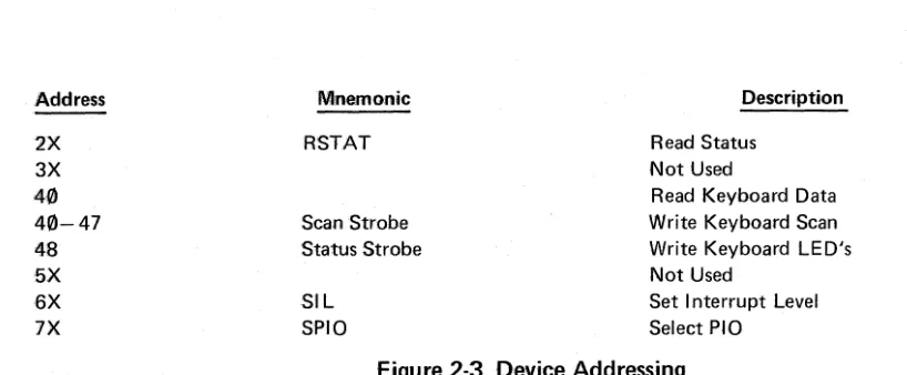
2.5 DEVICE ADDRESS DECODING
Chips U55 and U56 on sheet 7 decode the device addresses for I/O operation.
Address Mnemonic Description
00-0F SVTAC Select VTAC
10-11 Set Communications Baud Rate
12 - 13 SSIO Select Communications USART
14 - 15 SOSIO Select Printer USART
16 - 17 Set Printer Baud Rate
~
VISUAL TECHNOLOGY JNCOBf'OBATED, BAILROAD AVENUE, DUNDEE PARK, ANDOVEB, MA 01810
Address Mnemonic Description
2X RSTAT Read Status
3X Not Used
40
Read Keyboard Data40-47 Scan Strobe Write Keyboard Scan
48 Status Strobe Write Keyboard LED's
fiX Not Used
6X Sit Set Interrupt Level
7X SPIO Select PIO
Figure 2-3 Device Addressing
2.5.1 Keyboard Operation
The Visual 100/400 uses a capacitive scan keyboard which is arbitrarily encoded. This
alJowslanguage variation merely by altering keycaps. The V 1
PO
firmware assigns the
appro-priate ASCII code to the detected key. Operation of the keyboard is initiated by the Z80
sending a matrix address (40 - 47) via the scan strobe (sheet 7). Referring to the keyboard
schematic, 65-02131, th is address is loaded into Z2 and selects one of the vertical matrix
lines. Any and all of the keys along this matrix line is loaded into the detector chip Z1.
When the Z80 reads address 40 hex, this keyboard data is stored in chip U63 (sheet 7) and
read on the data bus. At the time this data is read, Latch Reset is also generated which will
reset the keyboard detector chip. In a similar manner, each vertical matrix line is selected
and keys are detected. The firmware reads a given key on four consecutive scans before it
determines validity and generates the code for that key. Status Strobe (48 hex) together
with its data bus bits are sent to keyboard to light the keyboard LED's and ring the bell.
2.5.2 PIO
The parallel input output chip (PIO) on sheet 9 of the schematics, provides three eight bit
channels operated in the output mode. Five bits of channel A (DT A0 - DTA4) are used to
determine the screen intensity. One bit of channel A (S80) alters the main timing chain for
80 or 132 character modes. One bit of channel A (VI DENB) inhibits video from reaching
the screen; one bit of channel A (PREV) selects screen presentation, Reversed or Normal.
Note that the character attribute REVERSE operates in addition to the screen REVERSE.
(A reversed character within a reversed screen appears as normal video).
Channel B of the PIO provides the scroll control count (SCC0- SCC3) which is used to
control smooth scroll and determines the scrolling region, when enabled. Three bits of
channel B (NVC1 - NVC3) are used to select the operating mode of the non-volatile RAM.
The last bit of channel B (BLKCUR) determines the appearance of the cursor (block or
underscore).
Two bits of channel C (NVCK,NVDO), provide the clock and data to the non-volatile RAM.
Three bits (RDE,LDE,TXDE) provide control for the communications interface. RDE
ena-bles receive data between the level shifters and the USART. LDE enaena-bles transmit data into
the receiver for local operation and for Local Echo operation when On Line. TXDE enables
the communications USART output data to reach the EIA and Current Loop level shifters.
VISUAL TECHNOLOGY INCORPORATED, RAILROAD AVENUE, DUNDEE PARK, ANDOVER, MA 01810
SPDS, another channel C output, drives pin 23 of the EIA interface, providing speed selec-tion when a modem, so equipped, is attached. One bit of channel C (SCRTS) provides secondary channel Request-to-Send signal on pin 11 or 19 of the E I A interface for use by modems having the secondary channel capability. The last bit of channel C (ACTS) enables received Clear-to-Send signal to be detected.
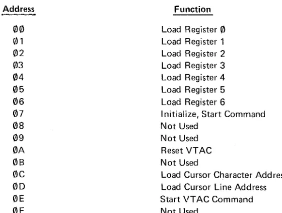
2.5.3 VTAC
The video timing and control chip, U32 sheet 2, provides all of the basic timing for the TV monitor. Beside generating horizontal sync. (HSYNC pin 15), vertical sync. (VSYNC pin 11) and composite sync. (CSYNC pin 10), it also provides an output defining the current char-acter line (pins 26 -
30),
the current raster line (slice) within the character line (pins 4,5,7 and 8), the current character count within the present line (VC0- VC7), present cursor position (pin 16) and a blanking signal (pin 17) which is used to blank the screen outside80
or 132 characters horizontally and outside of the 24 lines vertically.
The VTAC is initialized immediately after the completion of self test and after each time the terminal is reset. Switching between
80
and 132 character modes also causes the VT AC to be reinitialized. The following addresses (low order byte) are decoded within the VTAC and are used for the functions indicated.Address
00
0102
03
04
05
06
07
08
09
0A
08
0C
0D
0E
0F
Function
Load Register
0
Load Register 1 Load Register 2 Load Register 3 Load Register 4 Load Register 5 Load Register 6
Initialize, Start Command Not Used
Not Used Reset VTAC Not Used
Load Cursor Character Address Load Cursor line Address Start VT AC Command Not Used
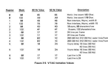
During initialize, registers 0 through 6 are set to the operating parameters as follows:
Figure 2-4 VT AC Addressing
VISUAL TECHNOLOGY INCORPORATED, RAI LROAD AVENUE, DUNDEE PARK, ANDOVER, MA 01810
Register Mode 60 Hz Value 50 Hz Value Description
0 80 65 65 Horiz. line count 102 Char.
0 132 A9 A9 Horiz. line count 170 Char.
80 4B 4B Non-interlace, Hsync, width 8
1 132 7B 7B Non-interlace, Hsync, width 15
2 80 4D 4D 10 scans, 80 characters/row
2 132 4F 4F 9 scans, 132 characters/row
3 80 17 17 24 lines per frame
3 132 17 17 24 lines per frame
4 80 02 1C 260 (60 Hz) 312 (50 Hz) raster lines/frame 4 132 02 1C 260 (60 Hz) 312 (50 Hz) raster lines/frame
5 80 10 2A Vsync delay 16 lines (60 Hz)
42 lines (50 Hz)
5 132 10 2A Vsync delay 16 lines (60 Hz)
42 lines (50 Hz)
6 80 17 17 Last I ine is 24
6 132 17 17 Last line is 24
Figure 2-5 VTAC Initialize Values
2.5.4 USARTS
The Visual 100/400 utilizes two Universal Synchronous, Asynchronous Receiver
Transmit-ter chips, one for the communications channel, and the other for the prinTransmit-ter inTransmit-terface. The
USART converts parallel data to serial for transmission, and converts serial data to parallel
for receive. It appends start, stop, and parity bits to transmitted data and checks received
data for presence and significance of these bits. The USART also generates modem control
signals Request-to-Send (RTS), Data-Terminal-Ready (DTR), and is used to detect modem
originated signals Clear-to-Send (CTS), and Data-Set-Ready (DSR). The USART also
gener-ates an interrupt, which can be enabled when the receiver has received a character, and/or
when the transmitter has finished sending a character. The data rate at which the receiver
and transmitter operate is determined by the baud rate generator which operates at 16 times
the baud rate selected. Schematic sheet 7 contains both data rate generators and both
USARTS.
2.5.5 Communications Interfaces
Sheet 9 of the schematic diagrams contains the logic for the E IA and current loop receivers
and transmitters. U86 and U 1 06 convert the RS232 level signals for both data and control
signals to TTL levels. Note that the modem control signals, CD,CTS,SCCD,DSR, and RI
have pull-up resistors connected to the nodes of their receivers. These resistors shift the
RS 232 threshold from ±3 volts to +2 volts and -4 volts. This causes control signals not
supplied by the modem (floating) to be detected as true. It is, as a result, not necessary to
jumper the EIA cable in order to force nonexisting control signals. Normally this threshold
VISUAL TECHNOLOGY INCORPORATED, RAI LROAD AVENUE, DUNDEE PARK, ANDOVER, MA 01810
shift presents no problems, as most interfaces operate with voltages significantly removed from the minimums (typically ±12 volts). Should an interface be encountered where signal levels are at the RS 232 minimums, the threshold of the receivers used, may be shifted back to standard levels by disconnecting the node pull-up resistor.
Transmitted E I A signals are generated by U96 and U 116. These drivers generate ±12 volt signals.
Received current loop data is converted by the optical isolator U74. Receive threshold is set to approximately 9 ma., yet the receiver is designed to receive data up to 50 mao 06 shunts current above 20 mao away from the MCT-2, preventing saturation at higher currents. Note that the output of the MCT-2 (U74) is coupled through switch U73-2 to the EIA receive input. EIA and current loop receivers can not be used simultaneously. Transmit data is converted to EIA levels (U96) and to current loop levels (U75) simultaneously. 04, 05, and CR8 provides 50 mao sinking capability on the current loop transmit output. Switch U73 provides selection between E IA and Current Loop interfaces, and selects active or passive current loop operation. Active current loop operation causes the terminal to supply the source of the current, while in passive mode the source of the current is external to the terminal.
Switch
U73-1
U73-2 U73-3 U73-4 U73-5 U73-6 U73-7
U73-8
2.5.6 Printer Interface
Function On
Alternate Character Generator PROM/ROM installed
Current Loop Mode
Passive Current Loop Receiver Active Current Loop Receiver Passive Current Loop Transmitter Active Current Loop Transmitter EIA pin 19 is Secondary
Request-to-Send EIA pin 11 is Secondary Request-to-Send
Figure 2-6 Communications Switch
Function Off
Alternate Character Generator PROM/ROM not installed EIA Mode
Active Current Loop Receiver Passive Current Loop Receiver Active Current Loop Transmitter Passive Current Loop Transmitter E I A pin 19 is not Secondary Request-to-Send
EIA pin 11 is not Secondary Request-to-Send
Sheet 9 details the printer port EIA level shifters, U116 and U106. These IC's are installed only when the printer interface is present. Connector J5 is.the rear panel connector. J4 is an internal PCB edge connector reserved for future use. Note that the printer interface is limited to EIA levels only and that the interface responds to a printer busy signal at EIA levels on connector pin 4.
2.6 NON-VOLATILE RAM
U45 shown on sheet 8 is the non-volatile RAM which is used to maintain SET-UP param-eters when the terminal is disconnected from power. U33, a DC to DC converter uses +5 volts to generate -23 volts used by the NV RAM. The PIO provides the clock (NVCK),
VISUAL TECHNOLOGY INCORPORATED, RAILROAD AVENUE, DUNDEE PARK, ANDOVER, MA 01810
data (NVDO), and mode control (NVC1 - NVC4). Data is loaded into and read from pin 12 of the NV RAM under control of the control of the three control lines detailed below. U47 shifts read data from
0
and +12 volts to TTL levels.Function NVC1 NVC2 NVC3
Standby
0
0
0
Address Enable
0
1 1Read Address
0
0
Sh itt Data Out 1
0
1Erase Data
0
0
Accept Data 1 1 1
Write Data 1 1
0
Not Used
0
0
Figure 2-7 Non-Volatile RAM Controls
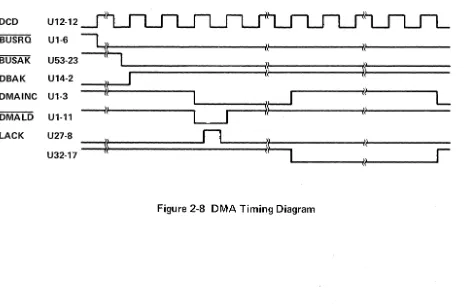
2.7 DMA
DCD
BUSRQ
BUSAK
DBAK
The DMA cycle is initiated at the beginning of each slice
0
(the start of each character line display) by flop U17 pin 5, on sheet 2. BUSRO (bus request) is generated for each line un-less inhibited by U17 pin 8. This inhibit is set after the DMA cycle begins for line 23 (last line) and is reset after vertical reset. The VT AC remains at a line count of 23 during vertical retrace, and would normally cause several DMA cycles serving no purpose. BUSRO is pre-sented to the Z80 which will relinquish the address and data buses at the end of the current instruction and acknowledges this by generating BUSAK (bus acknowledge).U
l?~~
~~
U14-2
---?~
it'
DMAINC Ul-3
~;
L
~~
(:'
L
I
1DMALD Ul-11 \
LACK U27-8
n
~~
U32-17=:::}~
III
NFigure 2-8 DMA Timing Diagram
VISUAL TECHNOLOGY INCORPORATED, RAI LROAD AVENUE, DUNDEE PARK, ANDOVER, MA 01810
Upon receiving BUSAK, DBAK is generated and the DMA cycle begins. Referring to the timing diagram for the DMA cycle in figure 2-8 and the U14 flops on sheet 2 of the schema-tics you will note that two DCD clocks occur before DMAINC (DMA increment) becomes active. The DCD clocks cause a video shift register load command (VSR LD) sheet 1, which causes the first byte of data to be loaded into chips U31 and U38 on sheet 3. The second DCD and VSR LD causes the contents of U31 and U38 to be transferred to U30 and U39. At the same time a second byte is loaded into U31 and U38. The output of these two sets of registers VD0-ACG Rand RB0-RB7 now contain a pointer to the location where the data to be displayed on this line of the screen is stored in RAM. On sheet 5, these two bytes of information are loaded into chips U51, U50, U52, through U60, U59, and U61 create the address of the data location. Line attribute clock (LACK), sheet 2, is generated at the same time. A delay, indicated by the blanking signal from the VTAC (U32-17), inhibits DMA in-crements (DMAINC) and data transfers until the character counter (VC0-VC7) gets to zero. Each character time hereafter, the address registers are incremented, the VT AC advances the character count (VC0-VC7) and causes data read from RAM to be stored in the DMA
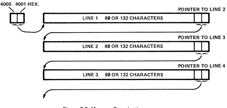
buffers U43, U42, and U41 on sheet 3. This operation continues until the VTAC reaches 80 or 132 characters and generates the blanking signal which inhibits gate U 1 on sheet 2 and causes DMAI NC to halt. DMAI NC stopping, leaves the address register U51, U50, and U52 set to the location where the next DMA cycle will find the next pointer bytes. Immediately after video blanking occurs HSYNC occurs which resets the bus request flop (BUSRQ) on sheet 2. This ends the DMA cycle and allows the Z80 to return to normal operation.
At the end of display of the last line of the screen, VSYNC occurs which causes the DMA address register (U51, U50, and U52) to be reset so that the pointer for the first lines' data will again begin at 4000 hex.
4000 4001 HEX.
" / POINTER TO LINE 2
1-1:J
1~
__________
L_I_N_E_1 __ 8_0_0_R __ 13_2_C_H_A_R_A_C_T_E_R_S ________~I-v-~I~I
~
f
---,/
P01NTER TO LINE 3I
LINE 2 80 OR 132 CHARACTERSI
I
J
--POINTER TO LINE 4
LINE 3 80 OR 132 CHARACTERS
Figure 2-9 Memory Organization
The first byte of the pointer becomes the low order address for memory. The second byte contains two nibbles. The low order nibble is used for the next higher 4 bits of the mem-ory address. The high order nibble is used to determine line attributes, Double Height, Double Width, Blanked, or Scroll.
VISUAL TECHNOLOGY INCORPORATED, RAILROAD AVENUE, DUNDEE PARK, ANDOVER, MA 01810
2.8 SMOOTH SCROLL
Smooth scroll is accomplished by scrolling one raster line each frame refresh cycle. The
multiplexer, U20 on sheet 5, provides control of scrolling for the entire screen or for that
region used when a scrolling region is defined. When a line is extracted from memory during
a DMA cycle which is within a scrolling region, U20 pin 1 is held at ground. This allows the
SCC0-SCC3 bits from the PIO to become the scroll counter bits (SCR0-SCR3). The PIO
counts from 6 to 15 (80 character mode) or 6 to 14 (132 character mode) each frame
re-fresh cycle, and only for those lines within the scrolling region. Whenever lines are
ex-tracted that are not in the scrolling region, U20 pin 1 is switched high forcing the scroll
counter bits to a fixed decimal value of 6. Whenever scrolling region is not enabled, the
firmware treats each line as if it were within the region. If scrolling region is not enabled,
then the scroll counter bits (SCR0-SCR3) are counted by the PIO from 6 to 15 (80
charac-ter mode) each frame refresh cycle. This value is added to the slice counts from the VT AC
by adder U8 on sheet 2. If the result of this addition is less than 15 (no carry), U7 adder
will add 10. When the first addition results in a carry, U7 adds 0.
Assuming that a normal line is being processed (not a double height top line), mUltiplexer
U6 passes this count unchanged. U5 added will add 0 if the current line is not the bottom
half of a double height line, resulting in slice counts VS0-VS3. These video slice counts
address the character generator PROM/ROM together with the character code to locate the
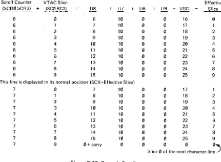
appropriate dot pattern. Figure 2-10 illustrates smooth scrolling during an 80 character line.
Scroll Counter VTAC Slice Effective
(SCR0-SCR3) + (SC0-SC3! U8 + U7 + U6 + U5 VSC Slice
6 0 6 10 0 0 16 0
6 1 7 10 0 0 17 1
6 2 8 10 0 0 18 2
6 3 9 10 0 0 19 3
6 4 10 10 0 0 20 4
6 5 11 10 0 0 21 5
6 6 12 10 0 0 22 6
6 7 13 10 0 0 23 7
6 8 14 10 0 0 24 8
6 9 15 10 0 0 25 9
This line is displayed in its normal position (SCX=Effective Slice)
7 0 7 10 0 0 17 1
7 8 10 0 0 18 2
7 2 9 10 0 0 19 3
7 3 10 10 0 0 20 4
7 4 11 10 0 0 21 5
7 5 12 10 0 0 22 6
7 6 13 10 0 0 23 7
7 7 14 10 0 0 24 8
7 8 15 10 0 0 25 9
7 9 0+ carry 0 0
o
0 0 )Slice 0 of the next character line .
Figure 2-10 Smooth Scroll
VISUAL TECHNOLOGY INCORPORATED, RAI LROAD AVENUE, DUNDEE PARK, ANDOVER, MA 01810
2.9 LINE ATTRIBUTES
U49 on sheet 5, stores the line attribute codes as each line is extracted during a DMA cycle. Scrolling Region (RB7), Logical Blanking (RB6), Double Width (DBW), Double Height Bottom (DHB), and Double Height (DHT) are decoded on sheet 5.
2.9.1 Scroll ing Region
Scrolling Region is discussed above in section 2.8.
2.9.2 Logical Blanking
The Logical Blanking is used by the microprocessor to inhibit video display of selected lines. Typically this is used during the display of the SET-UP modes to insure that the blank areas of the screen remain blank.
2.9.3 Double Height
The double height bit is set for both the top and bottom half of a double height line. It is used to alter the slice counts by halving the number and doubling the use of each of these slices. DHT switches multiplexer U6 on sheet 2 so that each of the slice bits are shifted to the next lower bit of significance, resulting in doubling the time of each slice count. When the input to U6 is counts 0 and 1 the output will be 0 and
0,
2 and 3 in results in 1 and 1 out. Slices 8 and 9 on the input results in slices 4 and 4 on the output. The output of U6 for a double height line, top or bottom half, is two slices each from0
through 4.2.9.4 Double Height Bottom
When the bottom half of a double height line is extracted during a DMA cycle, the slice counts, defined above for a double height line, are further modified by U5 on sheet 2. When double height bottom (DHB) is true, U5 adds 5 to the slice counts defined in sec-tion 2.9.3 resulting in the following sequence: 5,5,6,6,7,7,8,8,9,9.
2.9.5 Double Width
When a double width line is extracted from memory during a DMA cycle, DBW is set true (sheet 5). Double width modifies the main timing chain on sheet 1. The flop (VSCRI), U23 divides CK by 2 and creates an inhibit to the video shift register for every other CK, thereby doubling the time (width) of each dot. In addition, flop (VSRLD), U12, is set at character times 0,2,4 etc. instead of each character time. This doubles the time that the charac-ter code associated dots are available to the video shift regischarac-ter, thereby doubling the width of each displayed character.
2.10 VIDEO
Once the character generator PROM/ROM has generated the dots for a character they must be modified as a result of screen reverse (PREV), character reverse video (RVI D), blink (BLINK), and highlighted video (BOLD). Underline is treated similarly to the underscored cursor.
VISUAL TECHNOLOGY INCORPORATED, RAILROAD AVENUE, DUNDEE PARK, ANDOVER, MA 01810
On sheet 4 of the schematics, gate U64 allows dots (VSRO) through whenever logical blank-ing (LBLAN K) does not inhibit dots. If the cursor mode selected is underline (B LKCU R is false), a row of dots is forced at the cursor location (CURF) during slice 8 (SC8) by the top gate input of U64. Gate U57, output pin 3, creates the block cursor display (BLKCUR is true) by combining the cursor (DCUR) with the reversing inputs PREY and RVID. Because there is no slice count in this gating the cursor wi" appear as a block rather than an underline.
RVID and PREY act so that the cursor is the opposite video as compared to the character. U64, dots, are exclusive or'd with this cursor by U57 pins 11 and 13. This results in the video, at the cursor location inhibiting the block if the block is white on black, or enabling video if the cursor is black on white, thereby allowing both the cursor and the character to be visible.
The two U48 flops form a video divider creating three levels of intensity, low, average, and high. The bold, reverse, and blink gating combine with the video so that the bold video is presented at the highest level. Normal data is presented at average video levels. Blink of normal data switches between average and low levels. Blink of bold data switches between bold and average levels. 01 combines this video data with the composite sync. and provides a composite video output for an external monitor. 02 provides video drive for the internal monitor.
2.10.1 Screen Intensity
On sheet 4 of the schematics, the internal video driver, 02, has a ladder network attached to its collector. DTA0- DTA4 signals, generated by the Pia, provide 32 intensity levels for the screen.
2.11 SELF TEST
Each time the terminal is turned on and each time it is reset a self test is initiated. A check-sum is calculated for program memory and compared to a check-sum stored in the PROM/ROM. Should an error be detected the Z80 is halted. After passing the checksum test data RAM is tested, then the attribute RAM. Again the Z80 is halted whenever an error is detected. Upon completing the PROM/ROM and RAM tests the screen is initialized. The screen lack-ing intensity and cursor is an indication that self test has failed as in this case the VT AC is not started. Verification of a halted Z80 is available on pin 18 of the Z80. Pin 18 wi" be ground only when the Z80 is halted.
After the VTAC is initialized, a check is performed on the non-volatile RAM. If the
NVRAM is ok, stored parameters are utilized to define SET-UP parameters. If the NVRAM check detects an error, the bell is sounded 6 times and the firmware sets default values for SET-UP parameters. Operation of the terminal is permitted in this case, as the operator may alter these default parameters using the SET-UP modes.
The keyboard lights are used within the self test and can be used to determine the nature of the fault. The following chart illustrates the states of the LED's after the indicated fault has occurred.
VISUAL TECHNOLOGY INCORPORATED, RAILROAD AVENUE, DUNDEE PARK, ANDOVER, MA 01810
Fault LED Illuminated
Line Local Keyboard Lock 1 2 3 4
ROM X
RAM X X
RAM, Attribute X X X
RAM, Printer X X X
*DATA X X
*CONTROL X X
*These two errors are described below.
Figure 2-11 Self Test Fault Indications
2.11.1 Communications Tests
When the terminal is placed in ANSI mode and either a Current Loop Turn-around Con-nector or an EIA Turn-around ConCon-nector is installed, the Visual 100 can execute its own test including data, control signals and data rates.
EIA Test - Install EIA Turn-around Connector (Pin 2 to 3, 4 to 8, and 6 to 20). Set DIP switches 1 through 7 OFF, 8 ON. Set terminal on line in ANSI mode (ESC
<).
Type ESC[2;14y. A repeating pattern will be displayed until either a failure is detectedor
the SET-UP key is depressed. If a data failure occurs the Line and 2 LED's will be illuminated. If a control signal error occurs, the Line and 1 LED's will be illuminated.Current Loop Test - Install Current Loop Turn-around Connector (pins 7 to 17, and 18 to 25). Set DIP switches 2,3,6 ON, all others OFF. Set terminal on line in ANSI mode (ESC
<).
Type ESC[2;10y. The same repeating pattern will appear. Failure in this mode, (data) is indicated by the Line and 2 LED's being illuminated.2.12 JUMPER ASSIGNMENTS
Nine jumpers are provided on the Visual 100 PCB to alter the configuration. Figure 2-12 details the location of these jumpers described below.
Jumpers Wl-W6 are configured per the chart located on schematic sheet
8
as a function of the size of the PROM/ROM's installed in locations Ul08 through Ul15.Jumper W7 connects DC ground to chassis ground. This jumper normally is not installed.
Jumper W8 is installed when the printer interface logic is not installed.
SIMULATOR CLIP LEAD LOCATION
CHASSIS FROM POWER SUPPL V
Figure
2
-
12
Jumper LocationTO TV MONITOR
PRESENT ON V400 AND ON Vl00 WITH PRINTER OPTION
PRESENT ON V400
_~~~~'ONLV
PRESENT WITH PRINTER OPTION
PRESENT
WITH lJi; ... ~'" PRINTER
OPTION
W8
ABSENT WITH PRINTER OPTION
<
en
C ~
r
-1
m
()
I Z
o
r
o
Cl
-< Z
()
o
JJ"
o
JJ ~ -1m
o JJ ~
r
JJ
o
~o
~
<
m Z
C
m
o
c z o
m m
"
~ JJi'\
~
Z
o
o
<
m
JJ
s:
~o
00
<
en C
»
r
-I
m
()
I
Z
0
r
0
G)
-<
Z
()
0 JJ "tJ
0
JJ
»
-I
m
.0
JJ
~
r
JJ
0
-...J
»
0
»
< m
z C
m
0 C
Z
0
m
m
"tJ
»
JJ
l'
»
z 00
<
m
.JJ ~
»
~
~
0
"" VJeo
O,yj
eetrt"(~
tfl", ...
I
If
S',OO
u
M
-'-100-
co
1 -
03
VISUAL TECHNOLOGY INCORPORATED, RAILROAD AVENUE, DUNDEE PARK, ANDOVER, MA 01810
3.
SPARE PARTS AND TOOLS3.1
SPARE PARTSEach Visual 100/400 terminal is composed of four major subassemblies and is designed to
be serviced on site by replacing subassemblies only.
3.1.1 TV Monitor Subassembly
The Zenith model D 12 NK 21 monitor consists of the following subassemblies.
Description
Monitor Kit (total)
PCB
Flyback Transformer
CRT
& Yoke
(CRT is Panasonic 310JLB4N)
3.1.2 Keyboard Assembly
Zenith P.N.
D12NK21
A8046
A8438
F6348
Visual P.N.
MN 002-000
MN 002-002
MN 002-001
MN 002-003
One keyboard is used on the Visual 100/400. It is manufactured by KTC and carries the
following part numbers: KTC 65-2131-00, Visual KB 002-001. The Visual 400 keyboard is
part number KTC 65-2220-00, Visual KB 003-001.
3.1.3 Power Supply Assembly
One power supply is used which has the Visual part number PA-003-A01, or PA-005-A01.
3.1.4 Main PCB (Visual 100)
The main PCB (PA 002-A01) contains all logic except for character generator, firmware
and printer logic. These must be additionally specified when ordering spare PCB's.
PROM/ROM
Location
Part Number
Character Generator
U29
I C or E 241-001
Firmware
U108
IC or E 240-012
Firmware
U109
IC or E 240-013
Firmware
U110
IC or E 240-014
Firmware
U 111
IC or E 240-015*
The revision on all PROM/ROM's used as firmware must be the same.
*On early Visual 100 terminals the baud rate generator lacked 200 baud. As a result the
baud rate generator(s) in location U83 and U84 must be matched with the firmware
PROM/ROM U111, and the crystal Y2 as follows.
Crystal Freq.
5.0688 MHz
1.8432 MHz
BGR P.N.
8116
8116 - 020
PCB Assy No.
19
A01
A 11
U111 PROM/ROM
VISUAL TECHNOLOGY INCORPORATED, RAILROAD AVENUE, DUNDEE PARK, ANDOVER, MA 01810
3.1.4.1 Main PCB (Visual 400)
The main PCB (PA 002 - A40/A41) contains all logic except for character generators,
firm-ware and printer logic. These must be additionally specified when ordering PCB's.
PROM/ROM
Location
Part Number
Character Generator
U28
I C or E 241-002
Character Generator
U29
IC or E 241-001
Firmware
U108
IC or E 240-040
Firmware
U109
IC or E 240-041
Firmware
U110
IC or E 240-042
Firmware
U111
I C or E 240-043
Firmware
Ul12
IC or E 240-044
Firmware
U113
IC or E 240-045
Firmware
U114
I C or E 240-046
Firmware
U115
IC or E 240-047
The revision on all PROM/ROM's used as firmware must be the same.
3.2 SPARE SUBASSEMBLY RECOMMENDATIONS
To service 100 terminals by subassembly exchange, the following subassemblies should be
stocked at the quantities indicated.
Quantity
5
3
3
3
Description
Main PCB
Power Supply PCB
TV Monitor PCB
Keyboard
3.2.1 Active Component Recommendations
Part Number
PA 002-A01 (PA 002-A40 for
\IPA 003-A01
MN 002-002
KB 002-001 (KB 003-001 for V
The following listcontains all active components found on the Main PCB, the Power Supply
PCB, and on the Keyboard. Total quantities per terminal and recommended stocking levels
are indicated. The recommendations are based on one depot repairing subassemblies from
approximately 100 terminals. See Section 7 for TV Monitor components.
Part
Visual P.N.
Qty '!Terminal
Recommended Spares
74 LSOO
IC 000-000
3
15
74 LS02
IC 000-002
1
10
74 LS04
IC 000-004
4
20
74 LS08
IC 000-008
4
20
74LS32
IC 000-032
1
10
74LS51
IC 000-051
1
10
74 LS74
IC 000-074
4
20
74 LS83
IC 000-083
3
15
VISUAL TECHNOLOGY INCORPORATED, RAILROAD AVENUE, DUNDEE PARK, ANDOVER, MA 01810
Part
Visual P.N.
Qty.lTerminal
Recommended Spares
74 LS93
IC 000-093
2
15
74LS138
IC 000-138
4
20
74LS139
IC 000-139
2
15
74LS161
IC 000-161
3
15
74LS174
IC 000-174
1
10
74LS175
IC 000-175
3
15
74 LS245
IC 000-145
2
15
74 LS257
IC 000-257
2
15
74 LS273
IC 000-273
1
10
74 LS367
IC 000-367
4
20
74 LS368
IC 000-368
1
10
74 LS374
IC 000-374
1
10
7416
IC 010-016
1
10
7426
IC 010-026
2
15
74166
IC 010-166
1
10
74196
IC 010-196
1
10
74S00
IC 020-000
3
15
74S02
IC 020-002
1
10
74S04
IC 020-004
1
10
74S10
IC 020-010
1
10
74S64
IC 020-064
1
10
74S74
IC 020-074
4
20
74S86
IC 020-086
2
15
74S174
IC 020-174
1
10
74S175
IC 020-175
2
15
1488
IC 340-001
2
15
1489
IC 340-002
2
15
Z80(UPD 780)
IC 440-001
1
10
PIO(UPD 8255)
IC 440-002
1
10
VTAC(CRT5037)
IC 440-004
1
10
USART(UPD 8251)
IC 440-005
2
15
8214
IC 440-006
1
10
MCT-2
IC 340-004
2
15
2111A-2
IC 140-003
3
15
2114L-2
IC 140-004
12 (16 for V400)
30 (40 for V400)
ER1400
IC 248-001
1
10
TL479
IC 340-006
1
10
LM339
IC 340-007
1
10
lN914
DA 000-001
10
30
lN5401
DA 320-001
4
20
CR1
DA 350-001
4
20
MCL1301
DA 440-001
1
10
2N4901
TR 010-001
1
10
TIP32
TR 020-001
1
10
TIP34
TR 030-001
2
15
VISUAL TECHNOLOGY INCORPORATED, RAILROAD AVENUE, DUNDEE PARK, ANDOVER, MA 01810
PN3644
MPSA05
MPSA55
7805
7812
7815
7912
22-00950-003
22-00908-003
*8116
*8116-020
TR 000-001
TR 010-002
TR 000-012
UR 100-005
UR 000-012
UR 000-015
UR010-012
KEYTRONIC
KEYTRONIC
IC 340-004
IC 340-005
3
2
1
1
1
1
1
1
1
2
2
* Replace with whichever part was originally supplied.
3.3 TOOLS
15
15
10
10
10
10
10
10
10
10
10
In order to gain access to the Visual 100 and to replace any subassembly, only a cross-head
and common blade screwdriver are required. The following listed toots, or their equivalent,
are recommended for depot level where subassemblies are repaired.
Qty.
Description
Manufacturer
Part Number
1
Oscilloscope 30 MHz
Tektronix
465
1
Romaid 2700 ROM Simulator
MicroHnk
2700-716
with 716 Personality Module
1
Vl00/V400 TEST PROM
Visual
Vl00TEST
VISUAL TECHNOLOGY INCORPORATED, RAILROAD AVENUE, DUNDEE PARK, ANDOVER, MA 01810
4. TEST METHODS
Test procedures for use of the Romaid ROM Simulator and the V100
TEST
PROM are included with the test PROM. This combination allows the depot to exercise theZ80,
P10, VTAe, USART, and memory.VISUAL TECHNOLOGY INCORPORATED, RAILROAD AVENUE, DUNDEE PARK, ANDOVER, MA 01810
5. MNEMONIC LIST
MNEMONIC LIST
Source
Mnemonic
Source Chip
Schematic Page
Definition
ACGR
U30
3
Select Character Generator A
ACTS
U54
9
Auxiliary Clear-to-Send
ADB0
U60 & U53
5&7
Address Bus Bit 0
AT0
U67
6
Attribute Bit 0
BLANK V
U16
2
Video Blanking
BLINK
U40
3
Blink Attribute
BLKCUR
U54
9
Block Cursor
BOLD
U40
3
Bold Video Attribute
BTIME
U2
2
Blink Time
BUSAK
U53
7
Bus Acknowledge
BUSRQ
Ul
2
Bus Request
CD
U86
9
Carrier Detect
CK
Ul1
1
Clock 23,868 MHz
COMP VIDEO
Q1
4
Composite Video Output
CSYNC
U18
2
Composite Sync.
CTS
U85
9
Clear-to-Send
CURF
U13
2
Cursor Flop
DATACK
U88
7
Data Clock
DBAK
U14
2
Data Bus Acknowledge
DBW
U22
5
Double Width
DB0
Several
-
Data Bus Bit 0
DCB
U25
1
Decoded Character Clock B
DCD
U12
1
Decoded Character Clock D
DCE
U12
1
Decoded Character Clock E
DCUR
U27
2
Decoded Cursor
DHB
U66
5
Double Height Bottom Half
DHT
U49
5
Double Height
DIRVID
Q2
4
Video Output to Internal Monitor
DMAINC
Ul
2
"DMA Increment
DMALD
Ul
2
DMA Load
DSR
U86
9
Data Set Ready
DTA0
U54
9
Display Amplitude (Screen-Intensity)
DTR
Ul03
7
Data Terminal Ready
VISUAL TECHNOLOGY INCORPORATED, RAILROAD AVENUE, DUNDEE PARK, ANDOVER, MA 01810
MNEMONIC LIST (Continued)
Source
Mnemonic
Source Chip
Schematic Page
Definition
HALT
U53
7
CPU Halted
HSY
U32
2
Horizontal Sync
HSYNC
U18
2
Horizontal Sync Buffered
INT
U35
7
Maskable Interrupt
IORO
U53
7
I/O Request
KBPRES
KBD
7
Keyboard Present
KD0
U63
7
Keyboard Data Bit 0
LACK
U27
2
Line Attribute Clock
LATCH RESET
U46
7
Keyboard Latch Reset
L BLANK
U49
5
Logical Blanking (Set-up)
LDE
U54
9
Local Data Enable
MREO
U61 & U53
5&7
Memory Request
M1
U53
7
M1 CPU Cycle
NMI
U53
7
Non-maskable Interrupt
NVCK
U54
9
Non-volatile RAM Clock
NVC1
U54
9
Non-volatile RAM Control Bit 1
NVDI
U47
8
Non-volatile Data Input (To CPU)
NVDO
U54
9
Non-volatile Data Output
. PBUSY
U106
9
Pri nter Busy
PCLOCK
U21
1
Processor Clock
PDTR
U104
7
Printer Data-Terminal-Ready
PIPT
U105
7
Pri nter Interrupt
PRD
U106
9
Printer Receive Data
PREV
U54
9
Page Reverse Video
PXD
U104
7
Printer Transmit Data
RB0
U31
3
Rebuffered Memory Data
(Video)-RCVI
U85
7
Receive Data Interrupt
RD
U61 & U53
5&7
Read
RDE
U54
9
Read Enable
RESET
U25
1
Initialize Reset
RFSH
U53
7
Refresh (Memory)
RI
U106
9
Ring Indicator
RSTAT
U55
7
Read Status
RTS
U103
7
Request-to-Send
RVID
U40
3
Reversed Video
RXD
U95
9
Received and Xmitted Data
S80
U54
9
80 Character Mode
VISUAL TECHNOLOGY INCORPORATED, RAILROAD AVENUE, DUNDEE PARK, ANDOVER, MA 01810
MNEMONIC LIST (Continued)
Source
Mnemonic
Source Chip
Schematic Page
Definition
SC0
U32
2
Scroll Count Bit 0
SCC0
U54
9
Scroll Count Bit 0 (Scroll Region)
SCCD
U106
9
Secondary Channel Carrier Detect
SCR0
U20
5
Scroll Region Scroll Count Bit 0
SCRTS
U54
9
Secondary Channel Request-to-Send
SIL
U55
7
Set I nterrupt Level
SPDS
U54
9
Speed Select
SPIO
U55
7
Select PIO
SSIO
U56
7
Select SIO (USART)
STASTB
U56
7
Keyboard Status Strobe
SVTAC
U55
7
Select VTAC
TXD
U103
7
Transmit Data
TXDE
U54
9
Transmit Data Enable
U!L
U40
3
Underline Attribute
VC0
U19
2
Video Character Count Bit 0
VD0
U30
3
Video Data Bit 0
VIDENB
U54
9
Video Enable
VIDIPT
U35
2
Video Interrupt
VREF
R47
1
Voltage Reference (+5V)
VS0
U5
2
Video Slice Bit 0
•
VSRCI
U23
1
Video Shift Register Clock Inhibit
VSRLD
U12
1
Video Shift Register Load
VSRO
U76
3
Video Shift Register Output
VSYNC
U32
2
Vertical Sync
VSYNCA
U58
5
Vertical Sync Buffered
WAIT
U53
7
CPU Wait Input
WR
U53
7
CPU Write
+5
Q2
1
P.S. Sch. +5 Volts
+12
VRI
10
P.S. Sch. +12 Volts
+15
Q4
1
P.S. Sch. +15 Volts
-12
VR3
1
P.S. Sch. -12 Volts
-23V
U33
8
P.S. Sch. -23 Volts
VISUAL TECHNOLOGY INCORPORATED, RAILROAD AVENUE, DUNDEE PARK, ANDOVER, MA 01810
6.
I.e.
DATA SHEETS
Included in this section are specifications for the following I.C.'s.
IC/E 241-001
UPD 780
2114L-2
2111
UPD 8251
UPD 8255
8116-020
CRT 5027
8214
ER1400
Standard Character Generator
Z80 CPU
1K RAM
256X4 RAM
USART
PIO
Baud Rate Generator
VTAC
I nterrupt controller
Non-Volatile RAM
CCiFO 00. O. (I
00 01 02 03 04 05 06 07
++++++++++++ ++++++++++++ ++++++++++++ ++++++++++++ ++++++++++++ ++++++++++++ ++++++++++++ ++++++++++++
o
+ ++ +.+, ++ ++ ++ ++ ++ +1 + + + ** -I- + ** ** ** + + ** ** + + ***** + + ***** + + ** + + **** +
2 + + + **** + + ** ** + + ** ** + + ** + + ** + + ** + + ** ** +
3 + + + ****** -I- + ** ** ** + + ****** + + **** + + ** + + ** + + ** ** +
4 + + + ******** + + ** ** + + ** ** + + ** + + ***** + + ****** + + **** +
5 + + + ****** -I- + ** ** ** + + ** ** + + ** ***** + + ***** + + ****** + + + /::.. + + + **** + + ** ** + + ****** + + ** + + ** ** + + ** + + +
7 + + + ** + + ** ** ** + + ** + + **** + + ***** + + ***** + + +
!::: + + + + .j., + + ** + + ** + + 'lH; -;;.* + + ** + + +
9 -I- + + ;- + + + *~- + + .** + + '** ** + + ** + + + ++++++++++++ ++++++++++++ ++++++++++++ ++++++++++++ +.++++++++++ ++++++++++++ ++++++++++++ ++++++++++++
o
1 2
4
/::..
7
';:'
0::::: 0'::;' OA 0[: OC OD (IE OF
++++++++++++ ++++++++++++ ++++++++++++ ++++++++++++ ++++++++++++ ++++++++++++ ++++++++++++ ++++++++++++ + -I- -I- + + 'i- -I- 0'>* + +- + + + + ** + + ** + + + + ** ** + + ** ** + + ** + + -I- + + + ** + + ** + + ** + + *** ** -I- + ** ** -I- -I- ** -I- + + + + + ** + + ** +
-I- ** + + ****** + + **** + + ** + + + + + + ** + + ** + + ******** + + ** *** + + ** + + ***** + + ***** + + ******+ + ******+ + *********+ + ** + + ** ** + + ****** + + + + ** + + ** + + + + ** + + ** + + ** + + ** + + + + ** + + ** + + + + **
-I-+
*·*****Jt
+ + ** + + ** + + + + ** + + -<".l!- + + + + ** ++ + + ** + + ** + + + + ** • ~ ** + + + + ** + + + + ****** + + ** + + + + ** + + ** + -I- + + ** + ++++++++++++ ++++++++++++ ++++++++++++ ++++++++++++ ++++++++++++ ++++++++++++ ++++++++++++ ++++++++++++
10 11 12 1:::: 14 15 U::. 17
++++++++++++ ++++++++++++ ++++++++++++ ++++++++++++ +++.++++++++ ++++++++++++ ++++++++++++ ++++++++++++
o
+ *********+ + + + + + + + + + ** + -I- ** + + ** +1 + + -I- -I- + + + ;- + +- -I- .,."., ;- -I- ** '1- + ** +
2 + + + *********+ + + + + +- + + ** + +- ** ~ + ** +
:3 + + ;. ;. + + ;. + .j- + + ,:;.* -I- +- ,'i-·k + + ** +
4
+ + + + + *********+ + + + +- + ******+ + ***** +;. *********+5 ; . + + + + 4- + + + + j- ;:!-;* + + ** + + +
<::. + + + + + + + '*'~'*'lHH;'·**'~,+ + + + 'c';~ + +- -<,,* 'i- + +
7 +
+ +
+
.;-+ .;-+
.;- +
+ +
+ .+.
+ +
+
+-+ +
+ + + + + +
+ +
+ +
+ +
+ .• + + + ;.
+ +
+
CCiRl00_ 0_ I)
lA
iE:
1,--. '-' 1[1IE
1F++++++++++++ ++++++++++++ ++++++++++++ ++++++++++++ ++++++++++++ ++++++++++++ ++++++++++++ ++++++++++++
I) + + + ** + + + + + + + + +- + + + +
1 + + + ** + + ** + + ** + ~ + + ** + + **** + + +
2 + + + ** + + ** + + ** + + + + ** + + ** ** + + +
3 + + + ** + + ** + + ** + + ******** + + ******** + + ** + + +
4 + *********+ + ** + + ** + + ** + + ** ** + + ** + + ****** + + ** +
5 + ** + + ** + + ** + + ** + + ** ** + + ******** + + ** + + +
6 + ** + + ** + + ** + + ** + + **
**
+ + ** + + ***** + + +7 + ** + + ** + + ** + + ** + + ** ** + + ** + + **** *** + + +
8 + ** + + ** + + ******** + + ******** + + + + + + ** + + +
9 + ** + + ** + + + + + + + + -j.- + + + +
++++++++++++ ++++++++++++ ++++++++++++ ++++++++++++ ++++++++++++ ++++++++++++ ++++++++++++ ++++++++++++
20 2l 22 2:7:: 24 25 26 27
++++++++++++ ++++++++++++ ++++++++++++ ++++++++++++ ++++++++++++ ++++++++++++ ++++++++++++ ++++++++++++
o
+ ++ + + + + ++ ++ + + +.t- +1 + + + ** + + ** ** + + ** ** + + ** -I- + *** ** + + **** + + *** +
2 + + + ** + + ** ** + + ** ** + + ****** + + *** ** + + ** ** + + ** +
3 + + -~ ** + + ** ** + + ******* + + ** ** + + ** + + ** ** + + ** +
4 + + + ** + + + + ** ** + + ****** + + ** + +- **** + + +
5 + + + ** + + + + ******* + + **
**
+ + ** + + ** **** + + +6 + + + + + + + ** ** -I- -I- ****** + + ** *** + + ** ** + + +
7 + + + ** + + + +
**
** -I- + ** + + ** *** + + ******* + -I- +::=: + ++ ++ +-;- ++ +.~ ++ +-+- +
.:;J + ++ ++ ++ ++ ++ ++- + + + ++++++++++++ ++++++++++++ ++++++++++++ ++++++++++++ ++++++++++++ ++++++++++++ ++++++++++++ ++++++++++++
2::: 2':,} 2A 2E: 2C 2D 2E 2F
++++++++++++ ++++++++++++ ++++++++++++ ++++++++++++ ++++++++++++ ++++++++++++ ++++++++++++ ++++++++++++
o
+ ++ ++ ++ ++ ++ ++ ++ +1. + ** + -I- "~,* + -I- -I- + -I- + -i- + + + + + *.* +
2
+ ** + +**
+ + ** ** + + ** + .~ + + + + + + ** + 3 + ** + + ** + + **** -I- + ** + + + + + + + + ** +4 + ** + + ** + + ******** + + ******** + + + + *~****** + + + + ** +
5 + ** + + ** + + **** + -I- ** + + -I- + + + + + ** +
6 + ** + + ** + + ** ** + + ** -I- + *** + + + + *** + + ** +
7 + ** + + ** + + + + + +
**
+ + + + *** + +**
+::;: + + + + + + + ..;- + *.* -I- + + + + + +
9 -I- ++ ++ ++ -i-+ ++ ++ ++ +
'=l
c;; (> () ..-; er:: r:!:! ( .. ,) + ++
+ + + + + + + + ++
+ + + + r---+
;N.~t +
, + + + +
*
*
*
+*
*
+*
*
*
+*
* *
+*
*
*
+*
* *
+*
*-+-*
+ -+-+ + + + + + + -+ + + ++
+ + + + + + + + + + + +*
* *
+* *
*
*
4*
+*
*
*
+o
*
*
*
+~
*
*
*
+* * *
*
* *
*
*
*
*
*
~
+* *
*
+ + + + + + + + + + + + + + ++ +
+ + .+ + + + ~ +*
*
~*
+* * *
* *
*
+* *
*
+ ~*
*
*
~0~
*
*
~*
+~ ~
*
+* *
*
~* *
+* *
*
~ ~ + -+~ + + + + + + + + + +
~ ~ + + + ~ ~ + + + + T
+
,-+
~
t
":(
*
*
*
*
~* *
*
*
*
*
*
~ ~ ~*
*
~;( :.~: + + + + ++
+'*
-+-1- ~ +
+ +
~ ~ +
+
~ + + t + + + +i~+++++ + + +
+ -;- +
+ -I .. +, (',~! ..} (,", ..j" + ,,~ ",: '*: ):,: ~: :~( :,~: );~ -:~: )~.
,,;,: 'i':
* ,:" ,:':
:~,:,~: ~'..: )~.: ~r
:~,:
*
y.,;
*
*
,1::
*:
~,: + + + + + + + + + + ~ ~ + + + + + + + + + + .~. + -+ + + ..t. + + + + + +
+
+
f"oj
-+--,:',-, -+
+ ~.
"
'i: ).,~:
t: )~: ):,: ;l;~
~
*
*
*
*
~.
*
~*
*
*:
);< '*:*
*
*:
*
'*
*
*
*
* *
'*
+t
++
++
+
+
+
+ + -+ + + + + + 1- + + +
+
++
+ + + + + + + ++
+ ~,+
*
+~
* * *
* *
*
*
+
M
*
*
* *
* '*
*
*
*
*
+
+
*
*
+ + + + + + + + + + + + + + + -+ + + ++
+ + + + ++
+ + + +g!
.,.. + + + +* *
.*
* * * * *
'i:
*
* *
*:
*
:/(
*
'* *
* * * * *
* *
* *
*
+ + + + + + + + +
:::> v-i l>~ (1:1 q- If) ...(i f'.. (I) I) ..
+
+
+ + ++
++
+ ++
+
+
+
+ + ++ +
++ +
+ + +
++
LL.+(.) +
++
+ + + +*
* * *
* *
*
*
* *
*
* *
*
*
*
:0:<*
*
+ +
+
+ + + + r + + + + + + + + ++
+ + + + + + ++
+ + + ++
+ + + ++
'.J..!
+
C,)
+
+ + + + +
*
*
*
'"
+ + +*
*
*
*
*
:0:<*
* *
*
+ + + + + + + + + + + ++
1-+ + + ++
+ + + + + + + + + + + ++
+ Q+ \~,) ++
+ + + "~: :9:*
*
:a:"<:~,; )'.' )~(
*
*
*
*
*
:Q:*'
:.?: + + ++
+ + +-+ + + + + + + -+ + -1- + +
-+- +- + + -+- + -+- +
+
-1--+-~,
-I--+ +
'*
,;:; ;<,. + i" + ":"*
+ C) + :'?: ~\: +(,',-+-
*
*
+...J~ ir. j,c. ,),..
+
.
* '
~+
,,~+
+
++ +
+
+ + ++
+ + + + +.+- + +
+
-+-+
+ + + -+- +- + T +
1-+
-+-iX!
-+-(,"\ ..j..
.. +
-I-+
1-;;~:
;9-~,: :Q:
~, ~:
\~:
<