ABSTRACT
SHE, XU. Control and Design of a High Voltage Solid State Transformer and its Integration with Renewable Energy Resources and Microgrid System. (Under the direction of Dr. Alex Q. Huang).
Solid State Transformer (SST) has been regarded as one of the most emerging
technologies in the power distribution system. It has the advantages of low volume, low
weight, fault isolation, and potential additional functions, such as voltage regulation,
harmonic filtering, reactive power compensation, and etc. However, the involvement of large
number of power devices makes the control of SST a challenge. In addition, the high voltage
and high power hardware design of the SST is not easy, certain design methodology needs to
be developed. Furthermore, the cost of the SST is much higher than the traditional
transformer, how to justify this cost gap is also of great importance.
In this dissertation, a systematic literature review is conducted for the development of SST
in the future distribution system. The key components essential for the SST are reviewed and
different techniques are compared. It is pointed out that the SST consists of
multilevel/modular power converter structure with advanced power devices and magnetic
materials achieves best performance in terms of the size and efficiency in high voltage
operation condition. While the challenges, including control architecture and design
methodology, need to be addressed. In addition, the potential markets for SST need to be
In this research work, a three-stage modularized type SST based on Si IGBT is selected as
the research target aiming at developing advanced control technologies, design methodology,
and application areas of the SST.
The first part of the dissertation focuses on the analysis, control, and design of the presented
three-stage SST topology. First of all, the voltage and current sharing issues of the presented
SST topology are analyzed and addressed. Firstly, a new control structure and design
methodology is proposed for balancing the voltage of the rectifier stage by using the
feedback regulation. This controller minimizes the coupling effect between the voltage
balance controller and the original system controller. Therefore, the design of the original
system controller can be as easy as the two-level converter system, and the two controllers
will not interact with each other. Secondly, the modulation based voltage balance method is
also explored with extremely fast voltage balance response. The design of the control system
can also be regarded as a two-level converter system and the voltage balance is achieved by
choosing the most suitable switching pairs of the H-bridges. Thirdly, a current sensor-less
current balance controller is proposed for the parallel operated DC/DC stage. This method
does not need any additional current sensors and can achieve the power sharing among
converters of DC/DC stage well. Fourthly, a 3.6kV-120V/10kVA SST hardware prototype is
designed and demonstrated for the smart grid application. The proposed control methods in
chapter 3 and chapter 5 are adopted in this high voltage SST prototype. Various tests are
conducted to verify the key characters of the presented SST topology compared with the
The second part of the dissertation focuses the on the advanced application of presented
SST in the future renewable energy and microgrid systems. Firstly, a family of SST
interfaced wind energy systems are proposed with the integrated functions of active power
transfer, reactive power compensation, and voltage conversion. The proposed wind energy
system can effectively replace the traditional transformers and reactive power compensation
devices, therefore a highly compact and integrated system can be obtained and the cost of the
SST can be better justified. Secondly, a SST interfaced microgrid system and its centralized
power management strategy are proposed. The presented microgrid system can access the
distribution system without bulky transformers and can manage both the AC and DC grid
simultaneously, operating like an AC/DC hybrid microgrid. In this condition, SST plays as
an energy router, benefiting the future residential systems.
All the technologies proposed in this work are original and provide value information for
© Copyright 2013 Xu She
Control and Design of a High voltage Solid State Transformer and its Integration with Renewable Energy Resources and Microgrid System
by Xu She
A dissertation submitted to the Graduate Faculty of North Carolina State University
in partial fulfillment of the requirements for the degree of
Doctor of Philosophy
Electric Engineering
Raleigh, North Carolina
2013
APPROVED BY:
_______________________________ ______________________________
Dr. Alex Q.Huang Dr. Iqbal Husain Committee Chair
________________________________ ________________________________
ii
DEDICATION
iii
BIOGRAPHY
Xu She was born in Hunan, China. He received the B.S. degree in electrical engineering
(major) and B.A. degree in English (minor), with honor from Huazhong University of
Science and Technology, China, in 2007. He received his M.S. degree majored in power
electronics and motor drive with honor from the same university in 2009. He started to
pursue his Ph.D. degree in North Carolina State University in 2009.
From August 2009 to July 2010, he has been working on the modeling of the green energy
hub and DC microgrid project. Since August 2010, he has been working on the solid state
transformer project. He was the team leader of Solid State Transformer (SST) group and
Medium Voltage DC (MVDC) transmission group at Future Renewable Electric Energy
Delivery and Management (FREEDM) Systems Center. From May to August 2012, he was
an intern with high power conversion systems laboratory at GE global research center, US,
conducting research on next generation high voltage dc transmission (HVDC) system.
His research interests are high power/voltage converters and their industrial applications,
and renewable energy resources integration.
His role in the first job will be a research engineer (lead professional career band) in high
iv
ACKNOWLEDGMENTS
The life that is full of challenge and competition always attracts me, although sometimes it
is struggle and painful. I feel lucky to achieve what I am now with the help and encourage of
many people.
First of all, I would like to show my deepest gratitude to my Ph.D. advisor, Dr. Alex Q.
Huang, who gives me guidance to research work and consistent support to me and my family
during the past four years so that I can concentrate on my Ph.D. study. Dr. Huang gives me
enough trust to take the leading responsibility of developing the generation-I solid state
transformer, which is one of the most important and challenging project in the FREEDM
systems center, and enough freedom to explore my own research interests. I benefit a lot
from him not only in terms of broad vision of technology and insight understanding of the
technical problem, but also the great leadership and personalities. These will benefit me in
the future career.
The help from faculties and staffs in the FREEDM system center are appreciated. I would
especially thank my committee members, Dr. Iqbal Husain, Dr. Srdjan Lukic, and Dr. David
Lubkeman, who have given me lots of useful suggestions to improve the quality of this
dissertation. I would like to thank Mr. Rogelio Sullivan, Dr. Ewan Pitchard, Mr. Hulgize
Kassa, Ms. Colleen Reid, and Ms. Karen Autry, for their help of my study at FREEDM
systems center.
Thanks Dr. Spencer Muse from department of statics for serving as the graduate
v It is also my great honor to work with those talented teammates of the solid state
transformer group at FREEDM system center. Special thanks go to Dr. Tiefu Zhao, Dr.
Gangyao Wang, Dr. Xijun Ni, Fei Wang, Xunwei Yu, Yang Lei, Li Wang, Dr. Wenxi Yao,
and Chushan Li. We have worked day and night together, contributing and witnessing the
fast development of the group. In addition, I would like to thank Dr. Rolando Burgos, who
was an adjunct associate professor at FREEDM system center, for his guidance in research
and help in technical paper writing.
The friends and colleagues in FREEDM system center make the four-year study at NCSU a
memorable experience. I would like to thank Dr.Yu Liu, Dr.Wenchao Song, Dr. Liyu Yang,
Dr.Xiaopeng Wang, Dr. Xin Zhou, Dr. Jiwei Fan, Dr. Jun Li, Dr.Xiaohu Zhou, Dr.Rong
Guo, Dr. Zhigang Liang, Dr. Qian Chen, Dr. Yu Du, Dr. Pochih Lin, Dr. Zhengping Xi, Dr.
Sanzhong Bai, Zhuoning Liu, Dr. Zhan Shen, Dr. Edward Van Brunt, Sumit Dutta, Yalin
Wang, Yen-mo Chen, Xing Huang, Li Jiang, Xingchen Yang, Dr. Xiang Lu, Arun
Kadavaelugu, Nick Parks, Dany Fregosi, Ryan Meitl, Philip Funderburk, Mengqi Wang,
Gahzal Falahi, Kai Tan, Rui Wang, Elie Najm, Rui Gao, Suxuan Guo, Yizhe Xu, Xiaoqing
Song, Fei Xue, Chang Peng, Qi Tian, Dr. Wu Chen, Dr. Qiwei Lu, Yiyi Zhang, Lijun Zheng
and many others that I cannot list the name here.
My heartfelt gratitude goes to my parents for their love and support. I am growing up in a
happy family and I have a wonderful childhood. Thanks my brother and sister-in-law for
vi Lastly, I would like to thank my beloved wife Huan Hu, who have given up a lot and
sacrificed too much to support me. Your love and encouragement make this beautiful journey
a reality. I really enjoy the time with you!
This work is supported by Natural Science Foundation under the Award Number
vii
TABLE OF CONTENTS
LIST OF TABLES ... x
LIST OF FIGURES ... xi
Chapter 1 Introduction ... 1
1.1 The distribution transformer ... 1
1.1.1 Introduction of the distribution transformer ... 1
1.1.2 Characteristics of the distribution transformer ... 3
1.2 The solid state transformer concept ... 6
1.3 Dissertation outline ... 8
Chapter 2 Solid State Transformer Technologies and its Application in Power Distribution System: Review and Scope of the Work... 12
2.1 High voltage power devices ... 13
2.1.1 State-of-art technology ... 13
2.1.2 Recommendation for future work ... 20
2.2 High voltage and high frequency transformers ... 20
2.2.1 State-of-art technology ... 20
2.2.2 Recommendation for future work ... 27
2.3 Solid State Transformer topologies ... 27
2.3.1 State of the art technology ... 27
2.3.2 Recommendation for future work ... 35
2.4 Applications of SST in the future distribution grid ... 35
2.4.1 State of the art technology ... 35
2.4.2 Recommendation for future work ... 42
2.5 Scope of the work of the dissertation ... 42
2.5.1 Research background ... 42
2.5.2 Research objectives and challenges ... 44
Chapter 3 A New Voltage Balance Controller for the Cascaded Multilevel Rectifier Stage: Minimize the Coupling Effect ... 55
3.1 Introduction ... 55
3.2 Controllability analysis of the voltage balance controller ... 59
3.3 Modeling of system in d-q coordinate considering voltage imbalance ... 61
3.4 A New voltage balance controller with minimized effect to original system controller ... 68
3.4.1Theoretical analysis ... 68
3.4.2 Discussion on controller design procedure and effective voltage balance area ... 71
3.4.3 Comparison of proposed methods with previous methods ... 76
3.4.4 Potential of reactive power balance among H-bridges ... 80
3.4.5 Experimental results ... 81
3.5 Investigation of reference generation techniques of voltage-balancing controller ... 86
3.6Conclusion ... 90
viii
4.1 Introduction ... 92
4.2 3-D space modulation technique for cascaded seven-level converter ... 93
4.2.13-D space description for cascaded seven-level converter ... 94
4.2.2 Factors that affect the DC voltage balance ... 99
4.2.3 3-D space modulation ... 101
4.2.4 Discussion of proposed 3D space modulation ... 111
4.3 Simulation and Experiments Verification ... 112
4.4 Conclusion ... 122
Chapter 5 A High Performance and Low Cost Power Balance Controller for DC/DC stage .... ... 124
5.1 Introduction ... 124
5.2 A current sensor-less power balance controller for DC/DC stage ... 125
5.2.1 Power balance issue of the parallel operated DAB converters ... 125
5.2.2 Relationship between active component of duty cycle in rectifier stage and the transferred power ... 132
5.2.3 Novel cost effective power balance controller for the paralleled DAB converters ... 133
5.3 Simulation and experimental results ... 134
5.3.1 Simulation results... 135
5.3.2 Experimental Results ... 138
5.4 Conclusion ... 143
Chapter 6 Hardware Design and Demonstration of a 3.6kV-120V/10kVA SST for Smart Grid Application ... 144
6.1 Introduction ... 144
6.2 Power devices and switching frequencies selection ... 145
6.3 High voltage and high frequency transformer design ... 150
6.4 Input filter design ... 153
6.5 Gate driver design ... 154
6.6 Power supply for the IGBT gate driver in a cascaded structure ... 157
6.7 Other components ... 162
6.8 Universal control platform design ... 163
6.9 Hardware of the prototype and experiment set-up ... 167
6.10 Experimental results ... 169
6.10.1 Steady state operation of SST ... 169
6.10.2 Start-up of the SST ... 170
6.10.3 Verification of Voltage and current sharing of SST ... 171
6.10.4 Reactive power support to grid ... 173
6.10.5 Load change operation ... 174
6.10.6 Input voltage sag operation ... 175
6.10.7 Efficiency of the SST ... 176
6.11 Discussion of the design ... 177
6.12 Conclusion ... 178
ix
7.1 Introduction ... 179
7.2 System Description ... 181
7.2.1 Wind generation systems overview ... 181
7.2.2 A family of SST interfaced wind farm systems ... 184
7.3 System Case Study ... 185
7.3.1 A Three-phase SST for system evaluation ... 185
7.3.2 System study in SCIG driven WFs ... 188
7.4 Three phase SST topology suits for the proposed wind system ... 197
7.4.1 A Topology of a Modular Three-phase SST ... 197
7.4.2 Conceptual design and simulation of a 1MVA, 13.8kV-480V three phase SST . 199 7.4.3 Experimental results for verifying the SST functions... 203
7.5 Conclusion ... 206
Chapter 8 Integration of Solid State Transformer with Zonal DC Microgrids ... 208
8.1 Introduction ... 208
8.2 Proposed SST interfaced microgrid system ... 211
8.2.1 Existing AC and DC microgrid architecture ... 211
8.2.2 Solid Transformer based microgrid ... 213
8.2.3 Zonal DC microgrid concept ... 215
8.3 System description and converter control ... 215
8.3.1 Studied microgrid system description ... 215
8.3.2 Solid state transformer control ... 219
8.3.3 PV converter control ... 222
8.3.4 Battery converter control ... 224
8.4 Power management algorithm ... 225
8.5 System cases study ... 229
8.5.1 Passive grid interaction (mode 3) ... 230
8.5.2 Transition from passive grid interaction mode to active grid interaction mode (mode 2 to mode3) ... 231
8.5.3 Islanding mode (mode 8) ... 233
7.5.4 Islanding mode transition (mode 8 to mode9) ... 234
8.6 Conclusion ... 235
Chapter 9 Conclusions, Contributions and Future Work ... 237
9.1 Conclusions ... 237
9.2 Major contributions ... 240
x
LIST OF TABLES
Table 1-1 Typical dimensions of GE-PROLEC three-phase pad mount transformers ... 4
Table 1-2 Typical cost data of three phase, pad mount transformer ... 5
Table 2-1 Preferred blocking voltage of power devices in the distribution system ... 13
Table 2-2 Comparison of material characteristics of 4H-SiC and Si ... 16
Table 2-3 Switching loss comparison of devices ... 17
Table 2-4 Comparison of different magnetic materials ... 22
Table 2-5 Performance comparison of four SST topologies ... 31
Table 2-6 Comparison of the tolerances of impedance and turns-ratio of power transformer: ANSI/IEEE and IEC standard [79] ... 49
Table 3-1 System parameters ... 78
Table 4-1 Trend of DC voltages in each area when vab>0 ... 98
Table 4-2 Factors influence the DC voltage ... 99
Table 4-3 Switching pair in each layer ... 101
Table 4-4 Switching tablev >0ab ,is>0 ... 105
Table 4-5 Switching tablev >0ab ,is<0 ... 105
Table 4-6 Switching tablev <0ab ,is>0 ... 108
Table 4-7 Switching tablev <0ab ,is<0 ... 108
Table 4-8 System parameters for simulation ... 113
Table 4-9 System parameters for experiments ... 120
Table 5-1 Parameters of the system ... 135
Table 5-2 Parameters of the prototype ... 138
Table 6-1 Parameters of the modified SST ... 145
Table 6-2 Calculated parameters of the power stage ... 149
Table 6-3 Parameters of the transformer in the SST prototype [40] ... 153
Table 6-4 Other components in the final power stage design ... 162
Table 7-1 Parameters of a single SCIG ... 191
Table 7-2 Parameters of 120kV generator equivalent impedance ... 191
Table 7-3 Parameters of transmission line (three-phase PI section) ... 192
Table 7-4 Parameters of the designed three phase SST topology ... 200
Table 8-1 Battery pack parameters ... 217
Table 8-2 PV cell parameters (1kW/m2, 25oC) ... 219
Table 8-3 SST system symbols ... 220
xi
LIST OF FIGURES
Figure 1-1 Application of distribution transformer in modern power grid ... 2
Figure 1-2 Distribution transformer national efficiency standards of US: (a) Single phase transformer (x-axis: power (kVA); y-axis: Efficiency; BIL: Basic Insulation Level); (b) Three phase transformer (x-axis: power (kVA); ... 3
Figure 1-3 Configuration of Solid State Transformer ... 7
Figure 1-4 Organization of the dissertation ... 9
Figure 2-1 High voltage power semiconductor devices ... 15
Figure 2-2 Size comparison between Si IGBT and SiC MOSFET ... 17
Figure 2-3 10kV/120A SiC half bridge module using twelve 10kV/10A SiC DMOSFET and six 10kV/ 10A SiC JBS Diode [16] ... 18
Figure 2-4 Ultimate current and voltage ratings for future SiC power devices [24] ... 19
Figure 2-5 10kVA, 3.8kV-400V, 3kHz transformer based on amorphous core [40] .... 23
Figure 2-6 150kVA, 1.7kV-377.8V, 10 kHz transformer based on amorphous core [42] ... 24
Figure 2-7 350kW, 8kHz transformer based on nanocrystalline core [44] ... 24
Figure 2-8 Structure of coaxial winding transformer [39] ... 25
Figure 2-9 Different solenoidal transformer structures: (a) shell type; (b) core type; (c) matrix type ... 26
Figure 2-10 Topology classification of SST ... 30
Figure 2-11 SST in high voltage and high power system ... 30
Figure 2-12 UFNIFLEX SST topology for smart grid application ... 32
Figure 2-13 EPRI SST topology (with inverter stage) for DC fast charger application . 33 Figure 2-14 Basic unit of GE SST topology for substation application ... 34
Figure 2-15 ABB SST topology for traction application ... 34
Figure 2-16 Proposed future distribution-level system architecture ... 36
Figure 2-17 SST based tractions system ... 37
Figure 2-18 Wind energy system interfaced by SST ... 38
Figure 2-19 SST based DC fast charger ... 38
Figure 2-20 High frequency link UPQC structure ... 39
Figure 2-21 Hybrid distribution transformer ... 40
Figure 2-22 SST for smart grid integration... 41
Figure 2-23 Topology of a cascaded multilevel converter based three stage SST ... 44
Figure 2-24 Different control methods for the presented SST topology ... 45
Figure 2-25 Equivalent circuit at the output of rectifier stage ... 46
Figure 2-26 Equivalent circuit of the DAB converter ... 48
Figure 3-1 Generalized voltage balance control diagram based on feedback control loop ... 57
Figure 3-2 Controllability analysis of the voltage balance controller ... 60
Figure 3-3 Original N H-bridges cascaded multilevel rectifier ... 61
Figure 3-4 N H-bridges cascaded multilevel rectifier with hypothesized phase ... 62
xii
Figure 3-6 Small signal model of the system in the d-q coordinate ... 66
Figure 3-7 D-q coordinate controller for cascaded multilevel converter with N H-bridges ... 68
Figure 3-8 Proposed voltage balance controller for cascaded multilevel converter ... 71
Figure 3-9 Small-signal representation of the original-system controller ... 74
Figure 3-10 Comparison of 2 1 ( ) N d dci di i NEd v d = −∑ between proposed method and previous methods ... 80
Figure 3-11 DC voltage and reactive power balance among H-bridges ... 81
Figure 3-12 Hardware setup for experiments: A scaled down SST prototype ... 82
Figure 3-13 Experimental results of cascaded seven-level converter ... 84
Figure 3-14 Reactive power balance under unbalanced load condition ... 86
Figure 3-15 Soft-start algorithm of rectifier ... 87
Figure 3-16 Control diagram of cascaded rectifier under d-q coordinate ... 88
Figure 3-17 Comparison of different voltage reference for balance controller ... 89
Figure 4-1 Topology of presented SST topology used in 12kV distribution line with 6.5 kV Si IGBT ... 94
Figure 4-2 Cascaded seven-level converter ... 95
Figure 4-3 Three-dimensional control region of cascaded 7-level converter and operation plane ... 97
Figure 4-4 Possible operation areas when v is positive ... 98ab Figure 4-5 H-bridge converter DC voltage charge path ... 100
Figure 4-6 Sub-space division by different layers ... 102
Figure 4-7 Switching pair selection diagram when v >0ab ... 104
Figure 4-8 Switching pair selection diagram when vab<0 ... 107
Figure 4-9 Switching sequences for H-bridges ... 110
Figure 4-10 Control diagram for single-phase seven-level converter under single-phase d-q coordinate ... 113
Figure 4-11 Input voltage and current under different operating modes ... 114
Figure 4-12 DC bus voltages under balance situation ... 115
Figure 4-13 Voltage balance under unity power factor mode ... 116
Figure 4-14 Voltage balance under capacitive mode ... 117
Figure 4-15 Voltage balance under inductive mode ... 118
Figure 4-16 3D space modulation with 1kHz switching frequency ... 119
Figure 4-17 Cascaded seven-level converter prototype ... 120
Figure 4-18 Performance comparison of different voltage balance methods ... 121
Figure 5-1 Topology of DAB converter ... 126
Figure 5-2 Operation principle for DAB converter ... 127
Figure 5-3 Generalized current balance controller for DC/DC stage ... 128
Figure 5-4 Power balance controller for DC/DC converters [78] ... 129
Figure 5-5 Rectifier stage controller with common duty cycle ... 130
Figure 5-6 Power balance controller for DC/DC converters [77] ... 130
xiii
Figure 5-8 Current sensor-less power balance controller for DC/DC stage ... 134
Figure 5-9 Performance of the system without power balance controller ... 136
Figure 5-10 Performance of the system with power balance controller ... 137
Figure 5-11 A three-stage SST prototype ... 139
Figure 5-12 Experimental results without power balance controller: (a) Input voltage, current, PWM voltage, and High voltage DC link; (b) High voltage DC links; (c) Output DC voltage, AC voltage and current; (d) DAB leakage inductor current; 140 Figure 5-13 Steady state performance with proposed power balance controller: (a) Input voltage, current, PWM voltage, and High voltage DC link; (b) High voltage DC links; (c) Output DC voltage, AC voltage and current; (d) DAB leakage inductor current. ... 141
Figure 5-14 Dynamic performance with proposed power balance controller: (a) Input voltage, current, PWM voltage, and High voltage DC link; (b) DAB leakage inductor current and output AC voltage. ... 142
Figure 6-1 Topology and specification of a three-stage solid state transformer ... 144
Figure 6-2 Re-packaged 6.5kV/25A Si IGBT module ... 146
Figure 6-3 Characterization of the 6.5kV/25A IGBT ... 147
Figure 6-5 High voltage and high frequency transformer for DC/DC stage ... 152
Figure 6-6 Selected core and assembled input inductor (one unit) ... 154
Figure 6-7 Concept gate driver core 2SC0535T [115] ... 155
Figure 6-8 Designed high voltage IGBT gate driver based on Concept gate driver core 2SC0535T ... 156
Figure 6-9 Switching performances of the IGBT driven by the designed gate driver .. 157
Figure 6-10 IGBT gate driver power supply solution in cascaded structure ... 158
Figure 6-11 Alternative solution for power the IGBT gate driver by using ultra-isolation line frequency transformer for test purpose ... 159
Figure 6-12 Ultra-isolation transformer for the IGBT gate driver power supply ... 161
Figure 6-13 Test results of the rectifier stage with ultra-isolation transformer ... 162
Figure 6-14 Universal controller signal flow path ... 163
Figure 6-15 Universal control platform for SST prototype ... 164
Figure 6-16 Functional diagram of interface board ... 165
Figure 6-17 Functional diagram of local controller board ... 166
Figure 6-18 HMI interface for control and monitoring ... 167
Figure 6-19 3-D layout of the SST prototype ... 168
Figure 6-20 Assembled SST prototype ... 168
Figure 6-21Test set-up of SST ... 169
Figure 6-22 Steady state operation of SST ... 170
Figure 6-23 Start-up of the SST ... 171
Figure 6-24 Experimental results for 3.6kV-120V, 5.2kW load condition ... 172
Figure 6-25 Inductive mode operation of SST ... 174
Figure 6-26 Capacitive mode operation of SST ... 174
Figure 6-27 SST operation under load change: 5.2 kW-3kW ... 175
xiv
Figure 6-29 Efficiency of the SST prototype ... 177
Figure 7-1 Global cumulative installed wind power capacity from 1996 to 2012 [117] ... 179
Figure 7-2 WFs with induction generator interfaced by normal transformer ... 183
Figure 7-3 Proposed WFs with induction generators interfaced by SST... 185
Figure 7-4 Three-phase SST for control illustration ... 186
Figure 7-5 Control system for the three-phase SST in wind energy systems ... 188
Figure 7-6 Power system plus WFs used in the case study ... 189
Figure 7-7 Power characteristics of wind turbine ... 191
Figure 7-8 Electrical characteristics of WF under study ... 192
Figure 7-9 Simulation results of WF interfaced by conventional transformer ... 193
Figure 7-10 Simulation results of WF interfaced by SST ... 195
Figure 7-11 Integrating energy storage device in the proposed wind energy system with enhanced LVRT capability ... 196
Figure 7-12 Proposed high voltage high power three-phase SST ... 198
Figure 7-13 Single phase SST building block ... 199
Figure 7-14 1MW system operation under unity power factor ... 201
Figure 7-15 1MW, 0.5MVar capacitive mode operation ... 202
Figure 7-16 1MW, -0.5MVar inductive mode operation ... 202
Figure 7-17 PCC voltage before start-up of the SST ... 203
Figure 7-18 SST operation without capacitive power compensation ... 204
Figure 7-19 SST operation with capacitive power compensation ... 205
Figure 7-20 SST operation without inductive power compensation ... 205
Figure 7-21 SST operation with inductive power compensation ... 205
Figure 8-1 Integration opportunities for future building [148] ... 209
Figure 8-2 Typical AC and DC microgrid architectures ... 212
Figure 8-3 Functional diagram of SST ... 213
Figure 8-4 SST based microgrid architecture ... 214
Figure 8-5 Solid state transformer integrated with zonal DC microgrid ... 216
Figure 8-6 Discharge characteristics of battery pack ... 218
Figure 8-7 PV panel characteristics (1kW/m2, 25OC) ... 219
Figure 8-8 Control diagram of presented SST ... 221
Figure 8-9 Control diagram of PV boost converter ... 223
Figure 8-10 Control diagram of battery bidirectional buck-boost converter ... 225
Figure 8-11 Zonal microgrid operating modes and transitions ... 226
Figure 8-12 Intelligent energy management system diagram ... 227
Figure 8-13 Mode 3 key operating waveforms ... 230
Figure 8-14 Mode trasition (mode 2 to mode 3) key operating waveforms ... 232
Figure 8-15 Mode 8 key operating waveforms ... 233
1
Chapter 1
Introduction
1.1 The distribution transformer
1.1.1 Introduction of the distribution transformer
Power generation, transmission, and distribution are the three main constituents of the
modern power system, in which the transformer plays a most critical role [1]. Transformers
enable high efficiency and long distance power transmission by boosting the voltage to a
higher one in the generation side with the so called power transformer. In the distribution
system side, this high voltage is stepped down for industrial, commercial, and residential use
with the so called distribution transformer.
The distribution transformer provides final voltage transformation to the end users in the
distribution system, which usually with voltage level less than 34.5kV at high voltage side.
At the low voltage side, 120/240V split single phase system and 480V three phase systems
are usually adopted in the US.
The distribution transformer can be classified from different perspective of view. According
to the phase number, it can be classified into three phase transformer and single phase
transformer. According to the installation method, it can be classified into pole mounted
transformer and pad mounted transformer. The pad mounted transformers are installed for
2 mounted transformers are mounted on a utility pole. According to the insulation medium, it
can be classified into liquid-immersed transformer and dry type transformer.
The distribution transformers are widely used in various applications, such as renewable
energy resources integration, high power charge station, traction system, reactive power
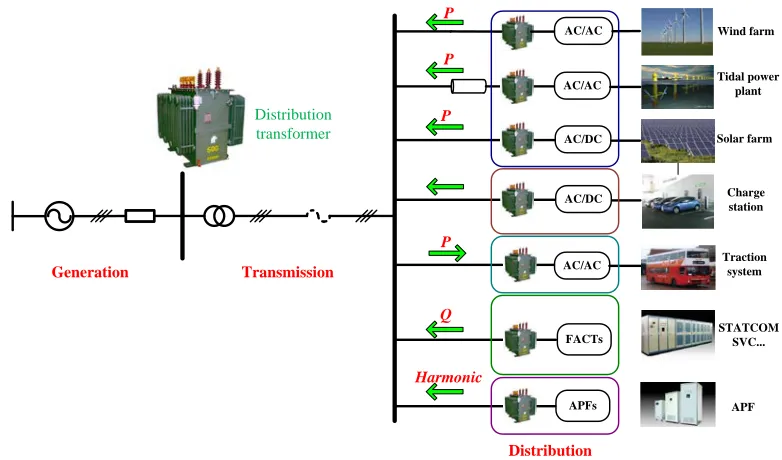
compensator, active power filter, and etc., as shown in Figure 1-1[2][3]. It functions as a
passive interface between the distribution system and the low voltage loads/sources.
Therefore, the voltage quality of the grid cannot be guaranteed if no additionally devices are
installed.
AC/AC
AC/AC
AC/DC
Wind farm
Tidal power plant
Solar farm
AC/AC Traction
system
FACTs
STATCOM SVC...
APFs
Generation Transmission
Distribution
P
P
P
P
Q
Harmonic
APF
Distribution transformer
AC/DC Charge
station
3
1.1.2 Characteristics of the distribution transformer
The US department of energy (DOE) released a standard for liquid and dry type distribution
transformers in October 2007, effective since January 2010[4]. This regulation covers all
distribution transformers manufactured after January 2010, and defines the minimum
efficiency standards as shown in Figure 1-2 for both single-phase and three-phase
transformers. It is seen that the overall efficiency of the distribution transformer required by
the standard is higher than 97 % irrespective of power rating, and this value approaches 99.5
% for most liquid-immersed power transformers. In addition, the standard calls for a higher
requirement for the liquid-immersed type transformer since it can transfer heat more
effectively, thus the core temperature does not rise as much, which would decrease
efficiency. Therefore, the first characteristic of the conventional distribution transformer is
high efficiency.
(a) (b)
Figure 1-2 Distribution transformer national efficiency standards of US: (a) Single phase transformer (x-axis:
power (kVA); y-axis: Efficiency; BIL: Basic Insulation Level); (b) Three phase transformer (x-axis: power
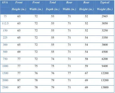
4 Table 1-1 lists the typical dimensions and weights of the GE-PROLEC three-phase pad
mount distribution transformer [5]. As seen, due to the large amount of copper and iron used,
traditional transformers are bulky, requiring space and incurring in high costs for
transportation. Hence, the second characteristic of the conventional distribution transformer
is heavy weight and low power density. Decreasing the volume and weight can bring
economic advantages to both manufactures and customers.
Table 1-1 Typical dimensions of GE-PROLEC three-phase pad mount transformers
kVA Front
Height (in.)
Front
Width (in.)
Total
Depth (in.)
Rear
Width (in.)
Rear
Height (in.)
Typical
Weight (lbs.)
75 63 72 53 71 52 2965
112.5 63 72 53 71 52 3050
150 63 72 53 71 52 3250
225 65 72 55 71 54 3350
300 65 72 55 71 54 3800
500 69 72 55 71 54 4500
750 77 72 74 71 58 6200
1000 77 75 75 71 59 9400
1500 77 76 76 77 67 12200
2000 87 78 79 71 69 13200
2500 87 78 79 71 69 13800
5 The standard costs for three-phase pad mount distribution transformers range from
$40/kVA to $100/kVA for size ranging from 50 to 150kVA[6]. Table 1-2 shows the typical
cost data for a three phase pad mount transformer. As can be seen, the cost of the
conventional distribution transformer is very low compared with the power electronics
devices. Therefore, the third characteristic of the conventional distribution transformer is the
low cost.
Table 1-2 Typical cost data of three phase, pad mount transformer
Size (kVA) 12.5kV 34.5kV
75 7749 10584
150 9450 11605
300 11718 15574
500 13608 20034
750 21257 21377
1000 25515 28350
Additionally as aforementioned, the conventional transformer is a passive interface between
high voltage and low voltage system. Therefore, the disturbances, such as voltage sag/swell
and harmonics at one side of the transformer will easily affect the other. From this
perspective of view, the fourth characteristic of the conventional transformer is the poor
voltage regulation and harmonic isolation capability.
The development trends of the traditional power transformers are mainly focused on new
6 factors. Nevertheless, new technologies need to be developed to considering the increasing
demand of the power quality and rapid development of the smart grid technologies.
1.2 The solid state transformer concept
Recently, together with other technological advancements, power electronics is being
seriously considered as one of the advantageous technologies that could empower future
smart grids, doing so at all levels of electrical power systems. Power electronics is one of the
key enabling technologies in electrical engineering nowadays. This is not entirely new, as
high power converters played an increasing role in both distribution and transmission power
systems over the past decades, for instance, in high voltage direct current (HVDC)
transmission systems and flexible ac transmission system (FACTs) devices, such as static
Var compensator (SVC), static synchronous compensator (STATCOM), unified power flow
controller (UPFC), and others [7]. Another portion of high power converters have found
increasing number of applications in renewable energy systems, especially in the case of
large penetration of renewable resources, such as solar and wind[8], [9].
In the recent decade, another high power converter, named solid state transformer (SST)
(also known as power electronic transformer or intelligent universal transformer), has caught
much attention and has been extensively investigated for distribution systems [10], [11], [12],
[13], [14], [15], [16]. The earliest concept of SST was introduced in [17], where it was
dubbed “electronic transformer”. Over the past few years, several efforts have been made to
7 are limited by power devices and circuit topologies, specifically in terms of their voltage
rating and efficiency, and as such have not penetrated into distribution systems.
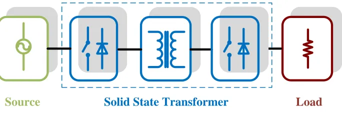
The SST is a power electronic device that replaces the traditional 50/60 Hz power
transformer by means of high frequency transformer isolated AC-AC conversion technique,
which is represented in Figure 1-3. The basic operation of the SST is firstly to change the
50/60 Hz AC voltage to a high frequency one (normally in the range of several to tens of
kilohertz), then this high frequency voltage is stepped up/down by a high frequency
transformer with significantly decreased volume and weight, and finally shaped back into the
desired 50/60 Hz voltage to feed the load. In this sense, the first advantage that the SST may
offer is its reduced volume and weight compared with traditional transformers.
Source Solid State Transformer Load
Figure 1-3 Configuration of Solid State Transformer
It is further seen from the configuration of the SST that some other potential functionalities
that are not owned by the traditional transformer may be obtained. First, the use of solid state
semiconductor devices and circuits makes the voltage and current regulation a possibility;
8 voltage sag compensation, fault current limitation, and others, which are not possible for
traditional transformers. Second, voltage source converters connected from the secondary
terminal of the SST could readily support a regulated DC bus, which could be connected to
DC microgrids enabling this new microgrid architecture.
Although the concept of SST is straight forward, its implementation is a challenge. The
SST is essentially a high power and high voltage power electronic circuit, of which the
operation is always a challenge from both hardware and control point of view. In addition,
SST contains many other components besides the high frequency transformer, such as power
devices, gate drivers, heat-sinks, control circuits, cooling system, auxiliary power, and other
ancillary circuitry. As such, the sought lower volume and weight reduction may not be
guaranteed without a careful design. In fact, the effectively decrease of the volume and
weight of the SST can be easier to achieve when the power rating is higher, in which
condition the transformer dominants the volume and the weight of the system. Furthermore,
in order to find more market drivers for the SST commercialization, new application areas of
the SST needs to be identified. Therefore, it is highly demand to look deeper into the SST
technologies and find better solutions.
1.3 Dissertation outline
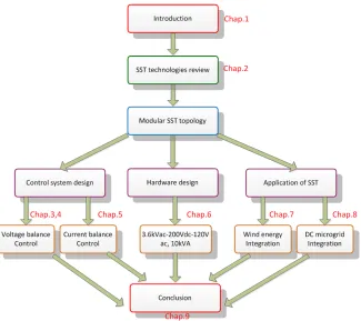
This dissertation focuses on proposing new control solutions, design methodology and
application areas for a modular, cascaded multilevel, three-stage SST topology. The
organization of the dissertation is shown in Figure 1-4 , in which three technical parts are
9
Figure 1-4 Organization of the dissertation
Specifically, the dissertation can be divided into nine chapters:
Chapter 1 provides the background and motivation of the proposed work.
Chapter 2 comprehensively reviews the key technologies essential for the development and
commercialization of the SST, including the power device, high frequency transformer,
circuit topology, and application areas. In each category, the technology challenges are
pointed out and recommendations for the future works are provided. A cascaded multilevel
three stage SST topology is picked as the research target and the control challenges are
10 transformer technology, can fulfill the demand of the high voltage and high power operation
of the modern power distribution system.
Chapter 3 proposes the voltage balance technique for the cascaded multilevel rectifier stage
by using the feedback control method, aiming at minimizing the coupling between the system
controller and voltage balance controller.
Chapter 4 proposes another voltage balance technique for the cascaded multilevel rectifier
stage by using the modulation strategy, which enables the ultra-fast voltage balance
capability.
Chapter 5 proposes the current balance technique for the parallel operated DC/DC stage. A
novel current sensor-less current balance strategy is proposed. The proposed method can
achieve the current balance controller without any current sensor in the DC/DC stage,
therefore is deemed to be cost effective.
Chapter 6 presents the hardware development of a 3.6kV-120V/10kVA SST prototype for
smart grid application. The presented design methodology is verified by experimental results,
providing useful experiences for the SST design.
Chapter 7 investigates the integration issues of the SST with renewable energy resources. A
family of SST interfaced wind energy systems with integrated functions of active power
transfer, reactive power compensation, and voltage conversion are proposed. The proposed
wind energy systems make fully utilization of the functions of the presented SST topology.
Therefore, the cost issues of the SST can be better justified.
Chapter 8 presents the integration issue of the SST with microgrid system. Specifically, a
11 proposed. The proposed microgrid system enables the power management among
distribution system, dc microgrid and ac microgrid, providing new solution for the future
residential system.
Chapter 9 concludes the major contributions of the dissertation and proposes the future
12
Chapter 2
Solid State Transformer Technologies and its
Application in Power Distribution System: Review and Scope
of the Work
Different from the conventional power electronic circuit, the SST combines the high
voltage, high power, and high frequency operation, which make the design and operation of
it a real challenge. As previously shown in Figure 1-3, the SST consists of power electronic
circuit and the high frequency transformer. From the circuit point of view, different power
devices can be combined with different circuit topologies for this application. In addition,
different core materials and transformer structures may be considered to build the high
frequency transformer. Furthermore, the SST can be applied in different areas, which are the
main market drivers for it. This chapter provides a critical review to the key technologies
essential for the development of the SST and correspondingly proposes the recommendation
for the future works[2]. Since the control of the SST depends on the topologies, therefore it is
not covered in this review. Lastly, a cascaded multilevel converter based three stage solid
state transformer topology is picked as the research target, and the correspondingly research
13
2.1 High voltage power devices
2.1.1 State-of-art technology
The existing SSTs are mainly targeted at the distribution voltage level, which ranges from
2.3 kV to 35 kV. In order to realize an efficient, highly compact, and reliable SST in the
distribution system, high voltage and high frequency operated power devices are necessary.
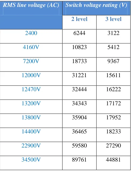
A recommended switch voltage rating based upon the practical guidelines for various
distribution voltages in both two-level and three-level based topologies is shown in Table
2-1, where the actual values may be different according to the design considerations [23].
Table 2-1 Preferred blocking voltage of power devices in the distribution system
RMS line voltage (AC) Switch voltage rating (V)
2 level 3 level
2400 6244 3122
4160V 10823 5412
7200V 18733 9367
12000V 31221 15611
12470V 32444 16222
13200V 34343 17172
13800V 35904 17952
14400V 36465 18233
22900V 59580 27290
14 Clearly, the switch voltage rating is quite high when it is applied in the distribution system
with simple two-level or three-level converters, and this poses a big challenge to the
development of SST. One possible solution is to adopt modular structures (series connection
of converters) or multilevel converters with low voltage and high speed power device [24].
The downside of this approach is that from a size reduction point of view, too many discrete
components increase the size and weight of the system. This is naturally not acceptable for
applications where these parameters are of importance. Alternatively, high voltage power
devices are under consideration, which can still be combined with the use of modular
topologies for very high voltage levels.
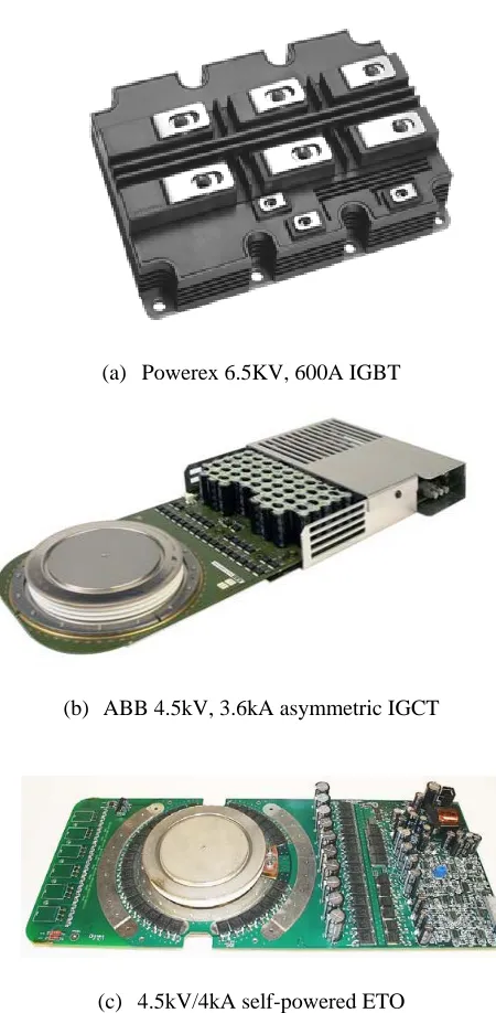
Figure 2-1 shows the high voltage insulated gate bipolar transistors (IGBT), integrated gate
commutated thyristors (IGCT), and emitter turn-off thyristors (ETO), which are suitable for
high voltage application. These devices can be used in some very high power applications.
However, they cannot operate at high switching frequency due to switching loss limitations,
and thus the practical switching frequency is generally lower than 1 kHz [25], [26]. This is
not feasible for the SST since the low switching frequency may not guarantee the effective
reduction of volume and weight in the transformer.
Series connection of low voltage power devices may therefore be one of the solutions for
high voltage operation. The penalty of this method is the large loop inductance intrinsic to
this configuration, which once again prevents the modules from operating in high frequencies
due to the additional induced voltage, which may damage the devices themselves as well as
15
(a) Powerex 6.5KV, 600A IGBT
(b) ABB 4.5kV, 3.6kA asymmetric IGCT
(c) 4.5kV/4kA self-powered ETO
Figure 2-1 High voltage power semiconductor devices
Integrated module packages of series connected power devices could be the solution to the
standard series connection discussed above [27], achieving minimum loop inductance and
16 resultant power module decreases the system efficiency, making it very hard to achieve
efficiency levels comparable to traditional 50/60 Hz transformers.
Wide band-gap materials, such as 4H-silicon carbide (4H-SiC) have been adopted for the
next generation post-silicon devices in high voltage applications. Table 2-2 lists the
characteristics comparison between 4H-SiC and Si (EBG: energy band gap; BEF: breakdown
electric field; TC: thermal conductivity; SEDV: Saturated electron-drift velocity). It can be
seen that SiC material has a larger energy band gap which makes it capable of operating at a
higher temperature. In addition, the 10 times larger breakdown electric field enables the SiC
devices to switch at higher voltage, higher current, and higher frequency condition. Both of
these two characteristics suit well SST applications.
Table 2-2 Comparison of material characteristics of 4H-SiC and Si
material EBG (eV) BEF(V/cm) TC (W/m.K) SEDV(cm.sec)
4H-SiC 3.26 2.2 (106) 380 2.0(107)
Si 1.12 2.5 (105) 150 1(107)
A systematic investigation has been done on high voltage SiC devices in smart grid
application [28]. 10-15 kV SiC MOSFET and IGBT (both P and N channel) have been
designed and evaluated, indicating that 10 kV SiC MOSFETs are the best choice for high
frequency applications above 2 kHz at room temperature, while IGBTs can handle higher
17 requirement of SST, the SiC MOSFET is preferred when the voltage is lower than 10-15 kV
due to its majority carrier conduction mechanism [28], [29], [30].
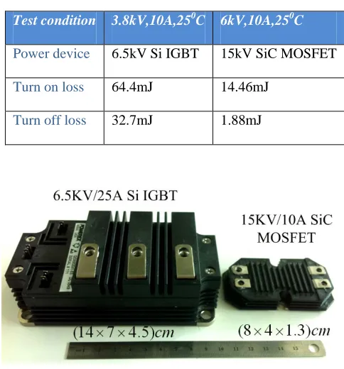
A 15 kV/10 A SiC MOSFET has been recently designed and fabricated by Cree Inc. The
loss data of the device was measured by using double-pulse test characterization. In addition,
a customized 6.5KV/25A Si IGBT was also tested in [14]. As a comparison, Table 2-3
presents the turn-on and turn-off loss of the 15 kV/10A SiC MOSFET and 6.5kV/25A
customized Si IGBT. It is shown that the SiC MOSFET can substantially reduce switching
loss, especially the turn off loss, thus can potentially boost efficiency. In addition, the weight
and size of SiC power device can also be reduced greatly, as shown in Figure 2-2.
Table 2-3 Switching loss comparison of devices
Test condition 3.8kV,10A,250C 6kV,10A,250C
Power device 6.5kV Si IGBT 15kV SiC MOSFET
Turn on loss 64.4mJ 14.46mJ
Turn off loss 32.7mJ 1.88mJ
18 In the applications where the high power is required, parallel operation of SiC MOSFET is
feasible due to its positive temperature coefficients for on-resistance. Figure 2-3 shows the
10kV/120A SiC half bridge module, which is adopted in a 1MVA solid state transformer
design [16].
Figure 2-3 10kV/120A SiC half bridge module using twelve 10kV/10A SiC DMOSFET and six 10kV/ 10A SiC JBS Diode [16]
Nevertheless, the on-resistance of SiC MOSFETs increases significantly as their blocking
voltage and operation junction temperature increase, making it unsuitable for applications
where the desired blocking voltage is higher than 10-15 kV [28]. In this condition, bipolar
devices such as SiC IGBTs play an important role due to their low conduction loss, moderate
switching time, superior high temperature operation, and excellent safety operation area
(SOA)—thus efficiency would not be compromised. The high resistance of p+ substrate
caused by incomplete ionization and low hole mobility in the n-channel SiC IGBT has been a
challenge, and efforts are mainly now on the P-channel SiC IGBT [31], [32], [33]. For high
19 switching speed, a result of the low current gain of the PNP transistor[34], [35]. 15 kV SiC
IGBT is being developed for a 100 kVA transformer-less intelligent power substation (TIPS),
in which the 20 kHz operation frequency will further decrease the volume of the system with
an expected efficiency of 98.4 % [36].
Finally, if the required current handling capability is larger (>1000A, >20kV), SiC GTOs
and thyristors with high switching frequency (10 kHz hard-switched and 100 kHz
soft-switched) will be most suitable [37].
Figure 2-4 gives the prediction of the ultimate current and voltage rating for future SiC
power devices [29]. It is concluded that SiC MOSFET will play an important role in the
application with voltage less than 15kV, whereas IGBT dominate the range from 15-20kV.
With operating voltage higher than 20kV, SiC GTO/Thyristor is the preferred choice.
20
2.1.2 Recommendation for future work
Advanced packages of series connected devices of commercial semiconductor chips is a
cost-effective solution considering the availability of SiC power devices. Wide band gap
power devices capable of high voltage and high frequency switching still need further
development. Although high voltage wide band gap devices have been reported, they are far
away from the optimized one and also cost significantly more than their silicon counterparts.
The issues of how to terminate the edge to support high breakdown voltage and how to
reduce the doping of drift layer have to be addressed [37]. In addition, in order to push the
power rating of SST to several MW and higher, high current devices and proper device
packages will also be needed. Furthermore, eliminating the use of oil means potential higher
operating temperatures, implying that high temperature power devices should also be
evaluated.
2.2 High voltage and high frequency transformers
2.2.1 State-of-art technology
The high frequency transformer is the main component in the SST, which replaces the
traditional 50/60 Hz transformer. In order to fulfill the high voltage, high power, and high
frequency operation requirements, many issues and challenges need to be addressed. First of
all, the selection of the magnetic material is critical to achieve high power density and low
loss in the transformer. In addition, its structure and winding configuration affect the
21 efficiency requirements. Furthermore, advanced thermal design is a challenge in order to
avoid the breakdown of the system for such a high voltage and high power system. Lastly,
the high voltage operation of SST makes the insulation requirement extremely strict,
especially when oil is eliminated and a compact design is required.
Several magnetic materials can be considered for high power applications, such as silicon
steel, ferrite, amorphous, and nanocrystalline[38], [39]. Table 2-4 shows the comparison of
different magnetic materials. Generally speaking, the silicon steel cores have high saturation
flux density and also high permeability. However, the loss of this material under high
frequency operation is high. Advanced silicon steel material can reduce the losses at high
frequency to a relatively low value, while the saturation flux density is also reduced.
Although the core loss of the ferrite core is moderate and the cost of it is low, ferrite cores are
not preferred in the SST application due to their low saturation flux density, which results in
a larger core size, conflicting with the high compact design requirement of the SST.
The Fe-amorphous alloy is a good choice for SST applications. The saturation flux density
of this material may be as high as 1.56 T and its loss is also moderate. In addition, large
cores, such as the C-type, are available, which suits well high power applications. However,
the loss of this material with operating frequency higher than several tens of kHz can only be
controlled by a low flux density, which leads to larger volumes. Another alternative is the
Co-amorphous alloy that has a much lower loss compared with Fe-amorphous cores,
22
Table 2-4 Comparison of different magnetic materials
Material Alloy
Composition
Loss (W/Kg)
(20KHz,0.2T)
Saturation
Bsat [mT]
Magneto-
striction (10-6)
Permeability
(50Hz)
4 μ -μmax
Max working
Tem.[oC]
Grain oriented silicon steel Fe97Si3 >1000 2000 9 2k-35k 120
Advanced silicon steel Fe93.5Si6.5 40 1300 0.1 16k 130
High performance ferrite MnZn 17 500 21 1.5k-15k 100/120
Fe-amorphous alloy Fe76(Si,B)24 18 1560 27 6.5k-8k 150
Co-amorphous alloys a Co73(Si,B)27 5 550 <0.2 100k-150k 90/120
Co-amorphous alloys b Co77(Si,B)23 5.5 820 <0.2 2k-4.5k 120
Co-amorphous alloys c Co80(Si,B)20 6.5 1000 <0.2 1k-2.5k 120
Nanocrystalline alloys I FeCuNbSiB 4.0 1230 0.1 20k-200k 120/180
Nanocrystalline alloys II FeCuNbSiB 4.5 1350 2.3 20k-200k 120/180
Nanocrystalline alloys III FeCuNbSiB 8.0 1450 5.5 100k 120/180
Overall, the nanocrystalline core is the best candidate among all for satisfying both the
power density and efficiency requirements. On the one hand, its saturation flux density is
much higher than ferrite—power density can be guaranteed, while on the other hand, its core
loss is the lowest among all the materials in question, promising high efficiency. Only two
important factors should be taken into account if the nanocrystalline core is considered. First,
the cost of this core is relatively high, thus it is not suitable when the cost is the dominating
limitation in the design. Second, the standard off-the-shelf core is toroidal uncut tape-wound
core, thus further modifications are needed if other core shape is needed.
Three 10 kVA, 3.8 kV to 400 V, 3 kHz transformers using the Metglas SA2605SA1
amorphous core have been demonstrated [40]. The results obtained indicated that 97 %
23 different high frequency transformers, specified at 100 kVA/20 kHz, 100 kVA/3 kHz, 33.3
kVA/20 kHz, and 33.3 kVA/3 kHz, were presented. The amorphous core was selected
achieving design efficiency higher than 99 %. Comparisons of different core materials for a
250 kVA, 5 kV to 380 V, 20 kHz transformer were conducted, and the conclusion showed
that nanocrystalline core achieves the best overall performance, while the amorphous core is
preferred under cost considerations [42]. A 150kVA/10kHz transformer based on amorphous
core was designed as shown in Figure 2-6.
24
Figure 2-6 150kVA, 1.7kV-377.8V, 10 kHz transformer based on amorphous core [42]
In order to achieve extremely high efficiency and ultra-compact design, the nanocrystalline
core VITROPERM 500F was investigated for a 1MW, 12 kV to 1.2 kV, 20 kHz transformer.
The efficiencies for different core configurations were calculated, estimating that the
efficiency could be as high as 99.99 % [43]. In [44], a 350kW, 8kHz transformer based on
nanocrystalline core was designed for the medium frequency railway system, as shown in
Figure 2-7.
25 Transformer structures are of equal importance in order to satisfy high power density and
high efficiency requirements. Generally speaking, there are two types of structures,
solenoidal and coaxial winding transformers [33]. The solenoidal is the most common
geometry of a transformer, in which the magnetic flux flows in parallel with the cylindrical
axis and the current encircles the cylindrical axis.
Figure 2-8 Structure of coaxial winding transformer [39]
In the coaxial structure, the flux encircles the cylindrical axis and the current flows in
parallel with the cylindrical axis [45], as shown in Figure 2-8. Although it is easy to control
and predict the leakage inductance of the transformer by using the coaxial structure, the
solenoidal structure is preferred in most design cases due to its advantages from a design
point of view, easier manufacturing, and lower cost [40], [41], [42], [43]. In addition, the
flexibility of the solenoidal structure in terms of turn ratio is better than the coaxial structure.
For both of these structures, multiple cores can be combined to build an equivalent larger
window area, which is suitable for high power and high frequency applications [40], [41],
26 Different solenoidal transformer structures are considered: namely core type, shell type, and
matrix type transformers as shown in Figure 2-9 [43]. The core type transformer provides
better insulation between the primary and secondary because of the inherent separation
between its two windings. Shell type transformers provide a higher degree of mechanical
protection to the winding because of the way the core surrounds it. In addition, a shell type
transformer magnetic circuit is equivalent to a parallel electric circuit, so it has a lower
reluctance compared to a core type transformer of similar cross-sectional area. In the high
voltage step ratio condition, the matrix-type transformer can be used by inter-wiring core
with series and parallel conductors [46], [47]. The manufacturing of the core type
transformer is the easiest and this configuration is adopted the most.
(a) (b) (c)
Figure 2-9 Different solenoidal transformer structures: (a) shell type; (b) core type; (c) matrix type
Another two factors that should be taken into account are the thermal and insulation
design, which are briefly introduced here. Compared with the conventional transformer, the
thermal and insulation aspects are much more difficult in the SST since much less space is
27 attractive solution if it is achievable [40]. However, different thermal dissipation methods can
also be adopted depending on the application, among which the fan-cooled and water-cooled
heat-sinks are the most common for high power density designs [43]. As to the insulation for
this dry type transformer design, suitable solid insulating materials, such as epoxy, have to be
inserted at the places where air is not enough for this high voltage and highly compact
transformer design [40],[41], [43]. In addition, high voltage insulation wire is also an
attractive candidate which significantly reduces the complexity of the transformer
construction [43].
2.2.2 Recommendation for future work
The high voltage and high frequency transformer is the key component in the envisioned
SST concept. Optimum design procedures should be further investigated to achieve high
efficiency and low volume designs based on existing core materials, wires, and insulation
means. It is also expected that better alloy optimization and process development can be done
such that new core materials can be used [42]. In addition, efforts can be directed to the
prediction of the parameters of the transformer, which is of great importance for higher
frequency operation. Lastly, low volume and weight is always the emphasis for the design,
28
2.3 Solid State Transformer topologies
2.3.1 State of the art technology
Numerous converter structures can realize the functions of isolated AC-AC conversion
thus potentially suit for SST application [10], [11], [12], [13],
[14],[16],[21],[36],[43],[44][24], [48], [49], [50], [51], [52], [53], [54], [55], [56], [57], [58],
[59], [60], [61], [62], [63]. In order to document these topologies, an approach to classify the
possible configurations has been presented [64], [65]. Considering possible conversion
stages, there are four basic topology configurations as shown in Figure 2-10, namely type A,
B, C, and D. Type A is the direct AC-AC conversion with transformer isolation to step down
from high voltage AC (HVAC) to low voltage AC (LVAC) [21],[48], [49], [50], [51]. In type
B, an isolated AC-DC conversion stage provides the low voltage DC (LVDC) followed by a
DC-AC conversion stage to provide the low voltage AC [52], [56],[58], [59], [60], [63] (the
topology in [52] can be categorized in either type B or C due to two isolated transformer
adopted). Type C also contains the two-stage conversion, in which the galvanic isolation and
voltage step-down are done by the DC-AC stage, therefore low voltage DC link is not
available [54],[62]. Type D is a three-stage conversion with high frequency isolation in the
DC-DC stage, thus both high voltage DC and low voltage DC link can be obtained [10], [11],
[12], [13], [14], [16], [24], [36], [43], [44],[53], [55], [57], [61].
In addition, considering the limitation of the power devices and magnetic components,
29 voltage and high power applications, as shown in Figure 2-11. Three possible connections
are illustrated, which are input series output parallel (ISOP), input parallel output parallel
(IPOP), and input series output series (ISOS). The input parallel output series (IPOS)
connection is not included since it is the same with ISOP in this application. It is worth to
point out that these SST configurations still fall into the four categories aforementioned from
the conversion stage point of view.
The proposals in type A present possible low cost and light weight solutions due to the
simple configuration. Four-quadrant power devices may be needed in case of bidirectional
voltage and current operating condition. However, the lack of DC link makes them
unsuitable for applications where reactive power compensation is required. In addition,
disturbances on one side may also affect the other side, which is the drawback of traditional
transformers. Type B and type C SSTs adopt two-stage configurations, with an isolation
stage in either the high or low voltage sides. Four-quadrant power devices are also needed on
the AC side of the isolation stage for bidirectional power flow. Compared with the type A
configuration, reactive power compensation is possible for type B and C SSTs if suitable
topologies are chosen. In addition, topologies in type A and B configuration are not suitable
for high voltage operation since zero-voltage-switching (ZVS) is hard to be guaranteed in
such a wide input range, and also mature multilevel topologies cannot be easily applied in the
high voltage side. In this condition, high switching losses may not be avoided without
sacrificing switching frequency, leading to lower efficiency and difficult thermal
management. Type C topologies may not face such a problem since lots of works have been
30 bus makes the integration of renewable resources on the low voltage (potentially residential)
side unfeasible.
HVAC LVAC
HVAC LVDC
HVAC HVDC
HVAC HVDC
LVAC
LVAC
LVDC LVAC
Type A:
Type B:
Type C:
Type D:
Figure 2-10 Topology classification of SST
SST cell
SST cell
SST cell
SST cell
SST cell
SST cell
ISOP IPOP
SST cell
SST cell
SST cell
ISOS HVAC
LVAC HVAC LVAC
HVAC LVAC
Figure 2-11 SST in high voltage and high power system
Most of the SSTs that have been designed for field application so far adopt the type D
31 room to optimize its performance in terms of efficiency, volume, and weight. Many attractive
features, such as VAR compensation, voltage sag compensation, renewable energy resources
and energy storage integration, and bidirectional power flow, may be potentially achieved.
Four well known high voltage SST designs, namely the UNIFLEX [10], EPRI [13], GE [16],
and ABB [67], are highlighted here since they have already been designed and fully tested
for different applications. Table 2-5 summarizes the performance comparison of these four
SST topologies.
Table 2-5 Performance comparison of four SST topologies
UNIFLEX EPRI GE ABB
Power rating 300 kVA 45 kVA 1MVA 1.2MVA
Phase number Three Single Single Single
Voltage rating 3.3 kV 2.4 kV 13.8 kV 15 kV
Transformer frequency 2 kHz 20 kHz 20kHz 1.8kHz
Eliminates oil No Yes Yes Yes
Var compensation Yes Yes No Yes
Voltage sag compensation Yes Yes No Yes
Voltage regulation Yes Yes Yes Yes
Harmonic isolation Yes Yes Yes Yes
Common DC link No Yes Yes Yes
Energy storage option Yes Yes Yes Yes
Fault isolation Yes Yes Yes Yes
Bidirectional power flow Yes No Yes No
Control complexity complicated Average Easy Average
Efficiency 92% 96% 98% 95%
Delivery Year 2009 2012 2011 2012
32 Figure 2-12 shows the UNIFLEX SST topology for smart grid application [10]. Basically,
it is a three-stage and three port power electronics converter used for universal and flexible
power management for future electricity network. The cascaded multilevel converter is
adopted as the front-end stage with several interleaving DC/DC converters as the
intermediate stage. It interfaces 3.3kV distribution level voltage with low voltage grids, such
as 415V system. Amorphous is adopted as the transformer core material and the operating
frequency is chosen to be 2 kHz. Oil is adopted for insulation and cooling for this medium
frequency transformer.
AC/DC/DC (cell 2) DC/AC
AC/DC/DC (cell N-1) DC/AC
AC/DC/DC (cell N) DC/AC
Interleaving DC links
Port 1 Port 2
Port 3
Figure 2-12UFNIFLEX SST topology for smart grid application
Figure 2-13 shows the EPRI SST topology for DC fast charger application. The
diode-clamped multilevel converter is applied for the high voltage side for both rectifier stage and
primary side of DC/DC stage, in which the 18kV/60A multilevel IGBT module by using the
33 secondary side of DC/DC stage to generate the low voltage DC link. The ferrite core is used
in the high frequency transformer with operating frequency of 20 kHz. In the DC fast charger
application, another high efficiency DC/DC converter is connected to interface with the
battery pack.
.
.
.
.
.
.
.
Figure 2-13 EPRI SST topology (with inverter stage) for DC fast charger application
Figure 2-14 shows the basic unit of GE SST topology for substation application. The
10kV/120A SiC half bridge module is adopted for the high voltage side and they are
connected in series to reduce the voltage stress. The switching frequency of the unit is chosen
to be 20 kHz and nanocrystalline core is therefore chosen as the core material for the
transformer to reduce the core l
![Figure 2-3 10kV/120A SiC half bridge module using twelve 10kV/10A SiC DMOSFET and six 10kV/ 10A SiC JBS Diode [16]](https://thumb-us.123doks.com/thumbv2/123dok_us/1217908.1153115/36.612.243.398.212.350/figure-sic-half-bridge-module-using-dmosfet-diode.webp)
![Figure 2-4 Ultimate current and voltage ratings for future SiC power devices [24]](https://thumb-us.123doks.com/thumbv2/123dok_us/1217908.1153115/37.612.224.407.411.563/figure-ultimate-current-voltage-ratings-future-power-devices.webp)
![Figure 2-7 350kW, 8kHz transformer based on nanocrystalline core [44]](https://thumb-us.123doks.com/thumbv2/123dok_us/1217908.1153115/42.612.221.410.467.609/figure-kw-khz-transformer-based-nanocrystalline-core.webp)