Atomic and Electronic Structure of Interfaces in Materials Systems for Future Semiconductor Devices
Full text
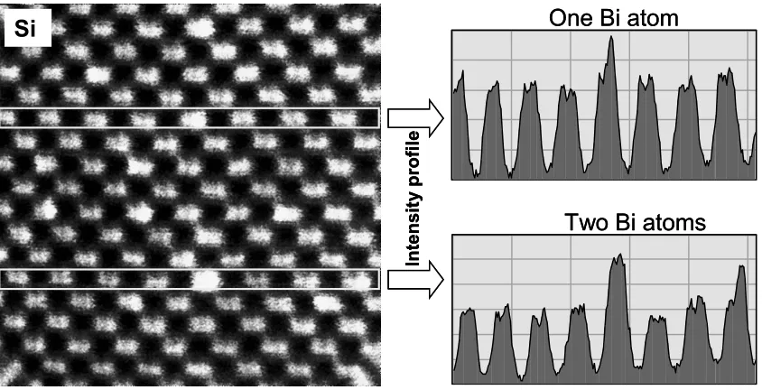
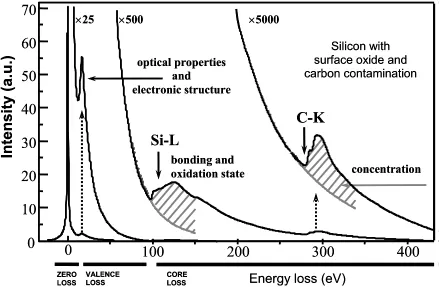
Figure
![Figure 2. Band offsets for high-κ dielectrics on Si (from [46]).](https://thumb-us.123doks.com/thumbv2/123dok_us/1235736.1156105/35.612.137.493.345.594/figure-band-offsets-high-k-dielectrics-si.webp)
![Figure 3. Dielectric constant κ versus band gap for candidate gate oxides (from [46]).](https://thumb-us.123doks.com/thumbv2/123dok_us/1235736.1156105/36.612.164.463.252.474/figure-dielectric-constant-versus-band-candidate-gate-oxides.webp)
![Figure 4. Dielectric constant κ versus optical bandgap EG of alternative gate dielectrics that are likely to be stable in contact with silicon (from [54])](https://thumb-us.123doks.com/thumbv2/123dok_us/1235736.1156105/39.612.142.488.145.412/figure-dielectric-constant-optical-bandgap-alternative-dielectrics-contact.webp)
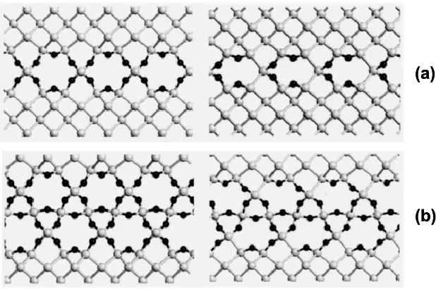
![Figure 8. The results of imaging of a Ge0.3Si0.7 alloy without aberration correction (a) and (c), and with aberration correction (b) and (d) (from [79])](https://thumb-us.123doks.com/thumbv2/123dok_us/1235736.1156105/50.612.179.455.307.570/figure-results-imaging-alloy-aberration-correction-aberration-correction.webp)
Related documents
To explore how the choice of observation sites influences the spatial variation of the sensible heat flux estimates, we define a set of pseudo-observation on Zufallferner (S1–S5;
Title: E-planning and collaboration : concepts, methodologies, tools, and applications / Information Resources Management Association, editor.. The framework recognises
Compared with the visit in last year, Professor Pompeo praised the rapid development of thoracic surgery in China, and said he was surprised to see the incredibly huge numbers
It lies at the base of Precambrian metamorphic rocks and tectonically separates the Salkhala unit of Precambrian age from the younger Panjal imbricate zone of Palaeozic– Mesozoic
average annual growth rate or CAGR for the number of BSBDA/No frill accounts opened over the past 5 years is 35% from 2009 to 2013. The growth rate over the period has
Aidha, utafiti huu umefanywa ili kubainisha jinsi, watunzi wa diwani ya Sauti ya dhiki na Msimu wa Tisa walivyotumia taashira ya mazingira katika kuwasilisha maudhui yao.. Taashira
Table 1 Details the static variables used to define the rearfoot, ankle, first ray, forefoot and hallux deformities investigated, the foot kinematic variab les used to compare feet
