
Resonant Gate Driver Design for High Efficiency Switching Power Converter.
131
0
0
Full text
Figure

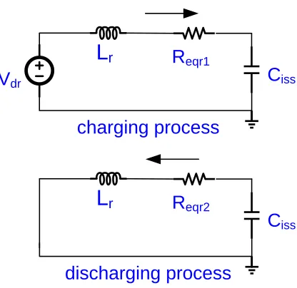
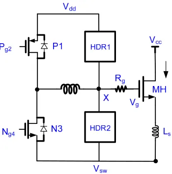
![Figure 2.2:Fig.2-4 (a) circuit for conventional gate driver of high side switch of buck converter; (b) equivalent circuit for high side switch driver for analysis [Yuming’04] (a) Circuit for conventional gate driver of high side switch of buck converter; (b)Equivalent circuit for high side switch driver for analysis [17]](https://thumb-us.123doks.com/thumbv2/123dok_us/1678589.1211570/27.612.184.442.104.585/conventional-converter-equivalent-circuit-conventional-converter-equivalent-analysis.webp)

+7



Outline
Review of the Basic Resonant Gate Driver Topologies
Impact of the Parasitic Source Inductance and Gate Resistance on VSD
Operation of the HD-CSD
Monolithic Solution of HD-CSD with Dynamic Biasing Back Gate Structure
Gate Drivers Control Logic Design for the Synchronous Buck Converter
Comparison of VSD, CSD and HD-CSD Drivers
Power Stage Setup of the Boost Converter
Gate Driver Test Prototype and Test waveforms
Power Efficiency Comparison of the VSD, 4S-CSD and HD-CSD in Boost
Future Work
Related documents