ABSTRACT
AYGÜN, SEYMEN MURAT. Processing Science of Barium Titanate. (Under the direction of Jon-Paul Maria.)
Barium titanate and barium strontium titanate thin films were deposited on base metal foils via chemical solution deposition and radio frequency magnetron sputtering. The films were processed at elevated temperatures for densification and crystallization. Two unifying research goals underpin all experiments: 1) To improve our fundamental understanding of complex oxide processing science, and 2) to translate those improvements into materials with superior structural and electrical properties.
This thesis next explores the ability to tune microstructure and properties of chemically solution deposited BaTiO3 thin films by modulation of heat treatment thermal profiles and firing atmosphere composition. Barium titanate films were deposited on copper foils using hybrid-chelate chemistries. An in-situ gas analysis process was developed to probe the organic removal and the barium titanate phase formation. The exhaust gases emitted during the firing of barium titanate films were monitored using a residual gas analyzer (RGA) to investigate the effects of ramp rate and oxygen partial pressure. The dielectric properties including capacitor yield were correlated to the RGA data and microstructure. This information was used to tailor a thermal profile to obtain the optimum dielectric response. A ramp rate of 20 °C/min and a pO2 of 10-13 atm resulted in a permittivity of 1500, a loss tangent of 0.035 and a 90 % capacitor yield in 0.5 mm dot capacitors. Yield values above 90% represent a significant advantage over preexisting reports and can be attributed to an improved ability to control final porosity.
Finally, the dramatic enhancement in film density was demonstrated by understanding the processing science relationships between organic removal, crystallization, and densification in chemical solution deposition. The in situ gas analysis was used to develop an each-layer-fired approach that provides for effective organic removal, thus pore elimination, larger grain sizes, and superior densification. The combination of large grain size and high density enabled reproducing bulk-like dielectric properties in a thin film. A room temperature permittivity of 3000, a 5 μF/cm2 capacitance density, and a dielectric tunability of 15:1 were achieved.
Processing Science of Barium Titanate
by
Seymen Murat Aygun
A dissertation submitted to the Graduate Faculty of North Carolina State University
in partial fulfillment of the requirements for the degree of
Doctor of Philosophy
Materials Science and Engineering
Raleigh, North Carolina 2009
APPROVED BY:
_______________________________ ______________________________
Jon-Paul Maria Zlatko Sitar
Associate Professor Professor
Materials Science and Engineering Materials Science and Engineering Committee Chair
________________________________ ________________________________
Gregory Parsons Yuntian Zhu
Professor Associate Professor
DEDICATION
BIOGRAPHY
ACKNOWLEDGEMENTS
First I would like to thank my mentor and friend Professor Jon-Paul Maria for the opportunities, guidance, and convincing me to pursue Ph.D. I am grateful for the four years I have spent at NCSU. I would also like to thank my friends at MSE; Jon Ihlefeld, Brian Laughlin, Mark Losego, Dipankar Ghosh, Spalding Craft, Patrick Daniels, Peter Gaifun Lam, Jimster, Erin Gross, Michelle Casper, Elizabeth Paisley, Jesse Jur, James Steel, and Tony Rice. I would like to acknowledge the help of Dr. Bill Borland with my research. I would like to thank Dick Parham and Edna Deas for their help and patience with my administrative problems.
TABLE OF CONTENTS
LIST OF FIGURES... viii
LIST OF TABLES ... xiii
CHAPTER 1. INTRODUCTION ...1
CHAPTER 2. LITERATURE REVIEW...3
2.1 Dielectrics ...3
2.2 Classification in Terms of Crystal Symmetry...11
2.3 Ferroelectricity ...13
2.3.2 Theory of Ferroelectricity ...14
2.3.3 Dielectric Properties of Ferroelectrics ...21
2.4 Perovskite Structure and The Archetypical Ferroelectric BaTiO3...31
2.4.1 Crystal Structure and Phase Transitions...31
2.4.2 Dielectric Properties...35
2.4.3 Compositional Modification with SrTiO3...38
2.4.4 Stress-Strain Effects...40
2.5 Scaling Effects in BaTiO3...43
2.5.1 Scaling Effects in Bulk BaTiO3...44
2.5.2 Scaling Effects in Thin Film BaTiO3...49
2.6 Processing of BaTiO3 – (Ba,Sr)TiO3 Thin Films ...57
2.6.1 Magnetron Sputtering...58
2.6.3 Firing of Thin Films on Base Metal Substrates ...81
References...85
CHAPTER 3. EXPERIMENTAL PROCEDURES ...104
3.1 Barium Strontium Titanate Sputtering on Base Metal Foils...104
3.2 Chemical Solution Deposition of Barium Titanate ...107
3.3 Low pO2 Processing of Thin Films ...109
3.3.1 Firing of Sputtered BST Thin Films ...109
3.3.2 Firing and Probing the Phase Evolution of CSD Barium Titanate Thin Films .112 3.3.3 Reoxidation Anneals ...116
3.3.4 Physical Characterization of the Thin Films ...119
3.3.5 Electrical Characterization of The Thin Films ...120
References...122
CHAPTER 4. HOT SPUTTERING OF BARIUM STRONTIUM TITANATE ON BASE METAL FOILS ...124
4.1 Hot Sputtering of Barium Strontium Titanate on Nickel Foils ...124
4.1.1 Introduction ...125
4.1.2 Experimental Procedure ...127
4.1.3 Results and Discussion...130
4.1.4 Summary...143
4.2 Hot Sputtering of Barium Strontium Titanate on Copper Foils...143
CHAPTER 5. PROCESS-PROPERTY RELATIONSHIPS IN CHEMICAL
SOLUTION DEPOSITED BARIUM TITANATE THIN FILMS ...154
5.1 Abstract ...154
5.2 Introduction ...155
5.3 Experimental Procedure...158
5.4 Results and Discussion ...161
5.5 Summary ...176
References...177
CHAPTER 6. HIGH DENSITY CHEMICAL SOLUTION DEPOSITED BARIUM TITANATE THIN FILMS...182
6.1 Experimental ...194
References...195
CHAPTER 7. CONCLUSIONS AND FUTURE WORK ...198
7.1 Conclusions ...198
7.2 Future Work ...199
LIST OF FIGURES
Figure 2.1 Schematic representation of dielectric polarization. ...4
Figure 2.2 Schematic representation of the frequency dependence of complex permittivity in the presence of various polarization mechanisms...9
Figure 2.3 Schematic representation of the spontaneous polarization as a function of temperature for a first order (a) and a second order (b) phase transition...16
Figure 2.4 Schematic representation of the polarization with a finite wavelength and infinite wavelength... 19
Figure 2.5 Schematic representation of (a) 180° and (b) 90° domain walls...20
Figure 2.6 Polarization vs. electric field curves for a single crystal ferroelectric, a polycrystalline ferroelectric, and a ferroelectric in the paraelectric state. ... 22
Figure 2.7 Relative permittivity vs. electric field curves for a ferroelectric and a paraelectric material...25
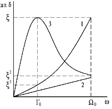
Figure 2.8 Schematic representation of frequency dependencies of (1) three-quantum, (2) four quantum, and (3) quasi-Debye mechanisms. o and o are the soft-mode frequency and damping... 30
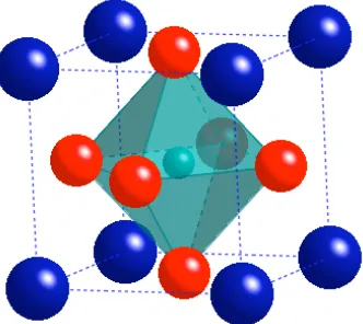
Figure 2.9 Perovskite unit cell shown with the BO6 octahedron. ...32
Figure 2.10 Cubic and tetragonal unit cells of BaTiO3. ... 34
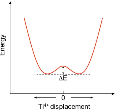
Figure 2.11 Schematic potential wells... 35
Figure 2.12 Dielectric constants Ka and Kc for single crystal BaTiO3. ...36
Figure 2.14 Curie temperature dependence of BaxSr1-xTiO3 on Ba concentration. ... 39
Figure 2.15 Dielectric constant of BaTiO3 as a function of grain size... 46
Figure 2.16 Temperature dependence of permittivity of BaTiO3 with changing thickness. ...47
Figure 2.17 Temperature dependence of permittivity of BST films with changing thickness. ... 55
Figure 2.18 Schematic depiction of magnetron sputtering... 59
Figure 2.19 Schematic plot of an amorphous CSD film, the supercooled liquid, and the crystalline perovskite phase... 73
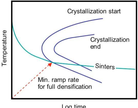
Figure 2.20 TTT and sintering curves for an amorphous material. ...76
Figure 2.21 Nucleation (Iv) and growth (u) rate data for anorthite. ...77
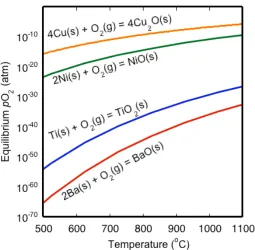
Figure 2.22 pO2 versus temperature diagram for the oxidation of metals... 83
Figure 3.1 Atomic force microscopy images of Cu and Ni foils. ... 105
Figure 3.2 (a) Schematic illustration of the sputtering system and (b) nickel and copper samples on a quartz plate... 106
Figure 3.3 Process flow for barium titanate chemical solution deposition. ... 109
Figure 3.4 Illustration of the system used for low pO2 firing. ... 112
Figure 3.5 Physical and chemical processes that occur during firing of a chemical solution deposited thin film. ... 113
Figure 3.6 Schematic illustration of the system used for in-situ experiments... 114
Figure 4.1 pO2 vs. temperature diagram showing the processing window in which the oxides of Ba, Sr, and Ti are stable with metallic Ni. ... 128 Figure 4.2 X-Ray diffraction patterns of the samples for (a) as-deposited and (b) fired at
900 °C... 130 Figure 4.3 Capacitance and loss tangent vs. field curves for the as-deposited samples
sputtered at 100 °C and 400 °C. ... 131 Figure 4.4 (a) Capacitance and loss tangent vs. field curves for the samples sputtered in
the range 100-400 °C (b) Tunability vs. sputtering temperature plot. ... 133 Figure 4.5 SEM surface image of the sample, which was sputtered at 400 °C (de-wetted
light colored areas are Pt)... 134 Figure 4.6 Field dependency of (a) Dielectric constant and (b) Leakage current density
of the sample sputtered at 400 °C. ... 135 Figure 4.7 Atomic force microscopy images of the samples sputtered at (a) 100 °C, (b)
200 °C, (c) 300 °C, and (d) 400 °C... 136 Figure 4.8 Temperature dependency of dielectric constant and loss tangent for the
samples sputtered at 100-400 °C. ... 138 Figure 4.9 Comparison of dielectric constant values as a function of crystal dimension
taken from several reports. ... 141 Figure 4.10 XRD patterns of the (a) as-deposited samples and (b) those fired at 900
Figure 4.12 Permittivity and loss tangent vs. field curves for the samples sputtered in the range of 100-300 °C... 147 Figure 5.1 Changes in the partial pressure of carbon dioxide as a function of time and
temperature for different flow rates. ... 162 Figure 5.2 (a) X-Ray diffraction patterns and (b) Raman spectra of the barium titanate
thin films... 165 Figure 5.3 Changes in the carbon dioxide partial pressure as a function of time and
temperature for the ramp rates of (a) 3 °C/min and (b) 1 °C/min... 166 Figure 5.4 Plane view images of the samples fired with (a) 20 °C/min, (b) 1 °C/min, and
(c) rapid ramp rates. ... 168 Figure 5.5 Cross-sectional images of the samples fired with (a) 20 °C/min, (b) 1 °C/min,
and (c) rapid ramp rates... 169 Figure 5.6 Permittivity versus applied bias curves for the samples fired with a ramp rate
of (a) rapid, (b) 20 °C/min, (c) 3 °C/min, and (d) 1 °C/min... 170 Figure 5.7 Changes in the carbon dioxide partial pressure as a function of time and
temperature for the oxygen partial pressures of (a) 10-15 atm and (b) 10-11 atm above 700 °C. ... 173 Figure 5.8 Plane view images of the samples fired at a pO2 of (a) 10-15 atm and (b) 10-11
atm above 700 °C... 175 Figure 5.9 Cross-sectional images of the samples fired at a pO2 of (a) 10-15 atm and (b)
atm and (b) 10-11 atm above 700 °C... 176 Figure 6.1 Plane view images of (a) one-step, (b) two-step, and (c) each-layer-fired
samples. ... 185 Figure 6.2 Cross-sectional images of (a) one-step, (b) two-step, and (c) each-layer-fired
samples. ... 186 Figure 6.3 Fracture images of (a) one-step, (b) two-step, and (c) each-layer-fired
samples. ... 188 Figure 6.4 (a) Permittvity vs. applied bias and (b) temperature dependent permittivity
curves for the three firing conditions. ... 190 Figure 6.5 Grain size dependence of permittivity comparison for pertinent data sets in
LIST OF TABLES
CHAPTER 1. INTRODUCTION
The ever-increasing advancements in electronic systems require continuous miniaturization of electronic circuits. As the sophistication and functionality of commercial and industrial electronics increase, the number of active circuit components such as integrated circuits (ICs) and passive components (resistors, inductors, and capacitors) must scale similarly and the price for each component must go down. For instance, the number of capacitors in a modern cellular phone has surpassed 500, while the average price has remained constant. This technology trend cannot be sustained using the conventional surface mounting approach. One avenue to shrink the size of these circuits is embedding passive components such as thin film capacitors within the printed wiring board. There are three main advantages of this method. First, surface space can be freed allowing more ICs; second, the inductive losses from metallization are reduced since the passive components can be located directly underneath the ICs, and third; the low cost of planar parallel processing compared to the series pick-and-place assembly. However, the lack of a reliable process for integration, insufficient capacitance density, and the cost issues stemming from expensive electrode materials has slowed down the progression of this approach.
thin films directly on base metal foils are discussed in addition to an expanded understanding of scaling effects in ferroelectric thin films. Process-property relationships are investigated by systematic selection and variation of three principle synthesis parameters: (i) thermal budget, (ii) atmosphere control, and (iii) thermal profiles for organic removal.
CHAPTER 2. LITERATURE REVIEW
2.1 Dielectrics
Dielectrics, also called insulators, are materials with a small number of charge carriers (<106 e-/m3) and large band gaps, Eg > 2.5 eV [1]. These materials can store energy by neutralizing charges at the dielectric/electrode interface in a capacitor [2]. This phenomenon is known as polarization, which arises from a finite displacement of positive and negative charges, i.e. formation of dipoles, under applied electric field. This is different from conduction, where there is a finite average velocity of charge motion under applied electric field.
If a dielectric material is inserted between the plates of a capacitor, it increases the charge storage ability per unit voltage by a factor of r, where r is the relative permittivity (or dielectric constant). Faraday was the first to recognize this increase in capacitance due to the polarization of the dielectric medium between the capacitor plates in the 1830s [3]. This can be pictured as the free ends of dipole chains neutralizing the opposite charges on the terminating metal plates, as shown in Figure 2.1. The dielectric material between the metal plates responds to the applied electric field by forming dipoles. Each dipole, which is a pair of opposite charges +q and –q, creates a dipole moment, which is given by
where q is the charge and d v is the charge separation (vector). Polarizability, which is the ability of an atom or molecule to become polarized, relates the dipole moment to the applied field through
p
v
=
E
v
Eq. (2.2)where is the polarizability. The sum of all the dipole moments gives the polarization, which is defined by
P
v
=
N
p
v
Eq. (2.3)where N is the number of dipoles per cubic meter. Ideally, the applied field, polarization, dipole moment, and separation vectors are parallel.
Figure 2.1. Schematic representation of dielectric polarization.
+
+
+
+
+
--
-
-
-
v
p
+
v
E
appliedP
v
In dielectrics, the material’s ability to polarize is quantified by the dielectric constant (or relative permittivity) or the dielectric susceptibility. The material polarizes by either creating dipoles or modifying existing fixed dipoles in linear dielectrics, or by reorienting re-orientable dipoles in non-linear dielectrics. The relationship between polarization and electric field is given by
v
P
=
o
E
v
or
P
v
=
(
r1)
oE
v
Eq. (2.4)where is the dielectric susceptibility, o is the permittivity of vacuum, and r is the relative permittivity.
It is also important to differentiate between free and bound (polarization) charges [4]. In Figure 2.1, the charges stored on the plates are free, since they are the electrons in the metal. On the other hand, the polarization charges in the dielectric are bound to the parent ion/atom cores. The free charge on the capacitor plates is Qo when there is no dielectric in between them. Under the application of an electric field, we may divide by the electrode area to define the electric flux density (or the dielectric displacement) as
v
D =
Q
oA
=
ov
E
Eq. (2.5)charge on the plates is Q= Qo+ QP. The free surface charge density on the plates after the dielectric inserted is given by
D =
v
P +
v
ov
E
Eq. (2.6)If the thickness of the dielectric is t, then the net capacitance is
C
=
orA
t
Eq. (2.7)dielectric/electrode interfaces or grain boundaries in the material. The dielectric constant of a material is the sum of all polarization mechanisms
r
=
r,el+
r,ion+
r,dip+
r,scif present 1 2 4 4 3 4 4
Eq. (2.8)
In general, covalently bonded materials, which only have electronic polarization, have very low permittivities (r<10), ionic bonded materials, which have electronic and ionic polarization mechanisms, have permittivities in the range 10-40, while materials with dipolar or space charge contributions can have permittivities exceeding 105. The magnitude of r also depends on the electronic structure, stiffness of the lattice, density, and defects.
When there is an alternating field (i.e. a sinusoidal wave, E=Eo sin(t)) applied across the capacitor, which is mostly the case in electrical circuits, the polarization of the dielectric leads to an ac permittivity. This complex permittivity is given by
*
=
ri
r Eq. (2.9)tan
=
rr
Eq. (2.10)
The phase difference between capacitor charging and discharging under an ac field (or the phase angle between the imaginary and the real components of permittivity) is 90o for perfect insulators with no loss and 0o for perfect conductors. Real capacitors have phase angle values in between these end points. Loss tangent is proportional to the heat generated per cycle. Therefore, at high frequencies this can become an issue.
Electronic and ionic polarization mechanisms can be thought as simple harmonic oscillators in which the driving force is the oscillating electric field and the restoring force is the Coulombic attraction between the species. These two mechanisms are active up to their resonant frequencies (el and ion), the point after which the oscillation of the electric field is too fast for them to respond. Electronic polarization is active up to very high frequencies, 1015-1016 Hz, since electrons have very low mass. Above the electron resonance frequency the material behaves no different than a vacuum (r~1). The ionic polarization is able to keep up with the oscillating field up to ~1012 Hz, the lattice vibration frequency, above which the restoring force and the mass of ions are too large to support a dipole formation that fast.
Dipolar polarization can be generically visualized as charged species jumping between the sites in a lattice. In the absence of an applied field these sites are equivalent,
however when a bias is applied a preference between the sites is generated. The collective of preferential jumps will then result in net dipole formation [5]. There are mainly two factors opposing the alignment of dipoles with the applied field. The first one is friction due to the dipole’s interaction with the neighbors during its rotation in a viscous medium. So, at high enough frequencies, megahertz to gigahertz region, the dipoles cannot follow the field, above this frequency range relaxation occurs. The reciprocal of the frequency (r) at which the polarization process can no longer respond is called the relaxation time (). This corresponds to the average time spent in each dipole orientation. The complex permittivity equations for dipolar polarization are given by the Debye relationships which include the relaxation time,
r=
+
o1
+
22 r=
(
o)
1
+
22 Eq. (2.10)where the real part of the permittivity r is a constant equal to o for frequencies <<r and equal to for frequencies above r. The Debye-model assumes one unique relaxation time
for the system which is a good approximation for crystals but not for glasses [6].
ionic polarization mechanisms, which are temperature independent. The reason is that dipolar polarization requires microscopic diffusion, in the electronic and ionic mechanisms, the charge displacement distances are so short that diffusion concerns can be effectively ignored. Space charge polarization occurs when the motion of charged defects can create net charge separation. There is no motion with an average velocity, however there is a finite displacement of charges since continuous current is impeded by insulating barrier(s). Often times this is the result of a heterogeneous structure such as combinations of an insulating phase & a conducting phase or insulating grain boundaries & conducting grains. All materials contain defects, impurities, various charge carriers, and heterogeneities, hence space charge is always present to a certain extent. Space charge gives rise to very high dielectric constants on the order of 104-106, however it is limited to low frequency applications (102-104 Hz). One common application of space charge polarization is the barrier layer capacitor. These are based on the limited reoxidation of a reduced material to obtain conducting grains and insulating grain boundaries [7]. As in the case of dipolar mechanisms, polarization involves a diffusional process, thus the temperature dependence is pronounced and a relaxation mechanism describes the frequency dependence.
2.2 Classification in Terms of Crystal Symmetry
The word “piezo” is derived from the Greek “piezein” meaning press or squeeze, hence piezoelectricity is the generation of a charge displacement under applied mechanical stress. This is known as the direct piezoelectric effect. The direction of the polarization (charge displacement) depends on the direction of the applied stress. The direct piezoelectric effect is defined using the tensor notation by,
P
i
=
d
ijkX
jk Eq. (2.11)where Pi is the polarization (a first rank tensor), dijk is the piezoelectric coefficient (a third rank tensor), and Xjk is the mechanical stress (a second rank tensor). These crystals also produce mechanical strain when they experience an electric field, which is known as the converse effect. Centrosymmetric crystals cannot be piezoelectric, because even under stress the center of positive and negative charges in a unit cell will still coincide and result in zero net polarization.
2.3 Ferroelectricity
2.3.1 A Brief History
The observation of polar materials possibly reaches back to Ancient Greece. More than 23 centuries ago, philosopher Theophrastos noted that lyngourion (possibly the mineral tourmaline) attracts wood particles [8]. The detailed work began with the advent of formalized crystallography in the 18th century, and pyroelectricity and piezoelectricity was discovered in Rochelle salt (NaKC4H4O64H2O) in the 19th century [9]. These findings enabled the discovery of ferroelectricity, when in 1921 Valasek reported that the spontaneous dipole moment in Rochelle salt can be reoriented by an external electric field [10]. The term ferroelectricity, which indicates polarization hysteresis with applied electric field, is used in analogy to ferromagnetism, which exhibits magnetization hysteresis with applied magnetic field.
[14]. The work of Wul and Goldman in the USSR and von Hippel in the US discovered that the origin of the high dielectric constant was ferroelectricity [15, 16]. There were also independent discoveries in Japan by Ogawa in 1944 and in England by Coursey and Brand in 1946 [17, 18]. The third significant step was the discovery of the poling process. Gray showed that a sufficiently high voltage can reverse the dipole moments of a ferroelectric ceramic [19]. These were followed by single crystal and then thin film studies. Today, ferroelectric materials find many application areas including high density capacitor applications, piezoelectric transducers, positive temperature coefficient resistors, and microwave filters with their interesting dielectric, piezoelectric, thermal, and optical properties.
2.3.2 Theory of Ferroelectricity
=
o+
T
C
T
o Eq. (2.12)where r is the relative permittivity, o is the permittivity of vacuum, C is the Curie constant, and To is the Curie temperature. Above the transition temperature, the crystal is in the paraelectric state, which is the non-polar state with no net dipole in the unit cell. Below the transition temperature, the material undergoes a phase transition into the ferroelectric state, a polar state with spontaneous polarization. If the transition is due to the displacement of the ions, then this is called a displacive transition. For example in BaTiO3, which has a cubic perovskite structure in the paraelectric state, the displacement of the Ti4+ ion from the cell center creates a dipole moment.
Ferroelectric transitions are generally classified into first and second order phase transitions. In a first order transition, spontaneous polarization exhibits a discontinuity at the transition temperature (Figure 2.3a), also there is a volume change and a latent heat associated with the transition. In a second order transition, the spontaneous polarization decreases continuously as the temperature decreases and reaches zero at the transition temperature as shown in Figure 2.3b. There is no volume change and no latent heat associated with the transition.
There are two main approaches to explain the microscopic origin of ferroelectricity and the ferroelectric phase transition [21]. The first one is the “polarization catastrophe” approach. In this model, at a critical temperature the local electric field caused by the dipole moment in the unit cell becomes larger than the restoring force stabilizing the polarization. Polarization is given by,
v
P
=
N
E
v
loc Eq. (2.13)where Eloc is not the external field, but the microscopic electric field felt by the polarizing atom. This Lorentz local field is given by,
v
E
loc=
E
v
+
1
3
ov
P
Eq. (2.14)Substituting Equation 2.14 into 2.13 and using Equation 2.4 to eliminate E v and P v , a relationship between r and is obtained,
r1
r+
2
=
N
3
o Eq. (2.15)This relationship is called the Clausius-Mossotti equation. Rearranging this gives,
r=
1
+
2
N
3
o1
N
3
oEq. (2.16)
This expression shows that when N
3o, r approaches infinity. So, when the product of number density and polarizability of the dipoles are at a critical level, the material becomes infinitely polarizable. This physically means that the dielectric will polarize even in the absence of an applied electric field. Neglecting electronic and ionic contributions the total polarizability is equal to the dipolar polarizability,
dip
=
v
p
2Substituting into Equation 2.16 we get,
rT
C
T
o Eq. (2.18)which is the Curie-Weiss law for the dielectric constant. This dipolar model predicts that as the temperature approaches the transition temperature from above, the permittivity becomes infinite, the system becomes unstable and a phase transition occurs. This divergence at To is called the polarization catastrophe.
Even though this dipolar model leads to the Curie-Weiss law for a ferroelectric transition, it has shortcomings when it is applied to polar liquids. For instance, according to this model the water should become ferroelectric at To = 1100 K [5]. However, water even does not become ferroelectric below its freezing temperature.
The other approach to explain ferroelectricity is associated with ionic polarizability. In ionic polarization, the permittivity can be related to the vibration mode frequency using a simplified version of the Lyddane-Sachs-Teller relationship by [22],
r1
TO2This relation suggests that if the lattice vibration frequency which produces polarization goes to zero, the permittivity reaches infinity. A specific transverse optic mode, known as the ferroelectric soft mode, displays a decrease in frequency as temperature decreases, and at the point that it becomes zero the host lattice becomes unstable and the ferroelectric phase transition occurs. When the frequency is non-zero (finite wavelength) the vibration of the ions will result in transient dipoles. However, the net instantaneous polarization will be zero since the oppositely oriented dipoles will cancel each other. The implication of the zero frequency is that when the wavelength becomes infinite, all the ions will be shifted from their equilibrium high temperature positions. The high temperature structure will be distorted into another structure and result in a net instantaneous polarization at any time as shown in Figure 2.4.
In the ferroelectric phase, the direction of polarization is not necessarily uniform throughout the material. The dipole moments in neighboring unit cells align themselves into regions of uniform polarization which are called ferroelectric domains. In the absence of an applied electric field, each domain will have a net polarization, however the average of all domain orientations will sum to zero. The polarization can be made uniform by the application of an external field in the paraelectric state and cooling with the field applied. This process is called poling, which can potentially reorient domains in the direction of the applied field. When an electric field is applied, the domains reorient so that there is a net polarization parallel to the applied field. Domain walls separate domain states and have a thickness that is dependent on wall orientation and material quality – in the absence of extrinsic factors, domain walls are only ~ 2 unit cells thick. The types of domain walls in a ferroelectric crystal depend on the symmetry. For example, while in a tetragonal perovskite 180° and 90° domain walls can occur, in the rhombohedral phase the polarization along the body diagonals result in 180°, 71°, and 109° domain walls [23]. The walls which separate the oppositely oriented domains are called the 180o walls (Figure 2.5a) and the ones which
separate the perpendicularly oriented domains are called the 90o (Figure 2.5b) domain walls. Key difference between them is the strain associated with the 90o domain walls.
Ferroelectric domains form to minimize the electrostatic energy due to depolarization fields and the elastic energy associated with spontaneous strain. Depolarization fields are required by any change in or gradient in polarity. This could be due to a change polarization near the surface or a gradient across a grain boundary. When the material experiences a phase transition mechanical constraints can increase the elastic energy by confining the spontaneous strain associated with the structural change. The formation of domains reduces the energy associated with both effects, however, 180 ° domain walls are only ferroelectric, while other domain wall orientations (like 90° walls) have also a ferroelastic component.
2.3.3 Dielectric Properties of Ferroelectrics
2.3.3.1 Polarization Hysteresis
ferroelectrics there is usually a large amount of stress in the material. This stress is relieved by 90o domain walls which results in lower switchable polarization values.
As the applied electric field is increased the domains start to align with the field and the measured polarization increases until all the domains become parallel to the field. This
point is called the saturation. When the applied field strength is decreased to zero, some of the domains switch back, however there is still a net polarization, which is called the remanent polarization, Pr. As the field is applied in the reverse direction, more domains switch back and zero polarization is reached when the electric field is at EC, coercive field, the amount of field needed to switch the polarization. Nevertheless, this is not an absolute value. If a lower electric field is applied for a sufficient amount of time, the polarization will eventually switch [24]. Spontaneous polarization can be found from the figure by drawing a tangent to the saturation and finding the polarization intercept. Since the P-E relation is hysteretic and the Equation 2.4 does not hold for the non-linear response, a definition in terms of the change in polarization could be written,
P
=
o(
r1)
E
Eq. (2.20)2.3.3.2 Dielectric Permittivity and Tunability
The dielectric permittivity of a ferroelectric material can be parameterized by Landau theory which is based on an expansion of the Helmholtz free energy with respect to polarization [25]. The first two terms of this expansion is given by,
F
=
2
P
2
+
4
P
4 Eq. (2.21)
Using the equation of state, F/P=E, taking the derivative of the above expression,
E
=
P
+
P
3 Eq. (2.22)Then, the dielectric permittivity can be written as,
r=
1
oP
E
=
1
o1
+
3
P
2 Eq. (2.23)capacitance-voltage (C-V) measurements. C-V measurements are small signal measurements where a small ac field (e.g. 0.05 V) superimposed with a dc field is applied. The oscillating voltage is used to measure the capacitance and then plotted as a function of the dc field. Generally, permittivity is calculated from capacitance, electric field is calculated using thickness, and the permittivity data are plotted as a function of the applied dc field. Figure 2.7 shows the typical r vs. E curves for a ferroelectric and a paraelectric material.
Measurements for ferroelectric materials are usually made with two sweeps, i.e. one from negative to positive bias and the other from positive to negative to show the hysteresis. The initial rise in the permittivity with applied field is due to the increased domain wall
movement which is locked-in by defects at zero bias and partial switching of the domains [26]. The maximum permittivity is observed when most of the domains are in the process of switching and the domain wall movement contribution to the polarization is maximum. At higher fields, the permittivity decreases due to two reasons. First, the number of domains and hence the domain walls decrease as they align with the dc field. Second, the oscillation of any residual domain walls is inhibited by the large dc bias. The only contributions to the permittivity at high fields are the intrinsic polarization mechanisms (e.g. ionic and electronic polarization).
In the paraelectric state the material does not exhibit any hysteresis, therefore the measurements can be made with a single sweep. A high permittivity is observed (at low fields), even though there are no domains or domain wall contributions. At temperatures not much higher than the transition temperature, the frequency of the lattice vibration mode TO (Eq. 2.19) is very low. At this point the restoring forces opposing the poling of the crystal are still weak, so the transient dipoles can interact with the applied ac field resulting in a high permittivity.
The change in permittivity with the applied field makes these materials attractive for high frequency voltage-tunable devices such as resonators, phase-shifters and microwave filters [25, 27-29]. The dependence of permittivity on the applied dc field is called the tunability. The tunability is defined as,
n
=
maxwhere max is the permittivity at zero field and min is the permittivity at saturation fields. Another way of defining tunability is the relative tunability which is given by,
n
r(%)
=
max min max•
100
Eq. (2.25)In general, the higher the permittivity the higher the tunability [25]. Tunability can be used as a means to compare the extrinsic response to the intrinsic response. For instance, for materials with the same composition, since the intrinsic (lattice) response would be similar, tunability might enable a comparison of extrinsic properties such as phase purity, homogeneity, microstructural properties (e.g. grain size), and crystal quality. This comparison will be used routinely in this thesis to evaluate material quality.
2.3.3.3 Dielectric Loss
Dielectric loss is a critical parameter in microwave applications since a figure of merit is defined based on dielectric loss and tunability for these devices, whereas in high capacitance density applications permittivity is of high importance [25, 29-31]. The dielectric losses in ferroelectric materials can be categorized as extrinsic and intrinsic contributions.
internal friction. Real materials contain charged defects, local polar regions, impurities and the interaction of these with the ac field also contributes to dielectric losses. Presence of defects can increase the conductivity of the material resulting in dielectric losses. Additionally, domain wall movement can also be clamped or pinned by these defects. These defects include oxygen vacancies and electrons trapped in the domain wall area, making the domain switching more difficult and hindering the domain wall motion [33].
In the paraelectric state there are no domains, so the dielectric loss is in principle much lower. For that reason, the non-polar paraelectric phase is used for high frequency applications where low loss tangent is crucial. The other extrinsic mechanisms play a similar role in the paraelectric state. The second group of phenomena that contribute to the dielectric loss is the intrinsic mechanisms. The following is a very brief summary of the models that were derived to explain their origins [25, 34, 35].
2.3.3.4 Dielectric Properties of Ferroelectric Thin Films
The dielectric properties of ferroelectric thin films are usually different than that of their bulk counterparts. Typically, thin films exhibit lower dielectric permittivity and higher loss tangent than the bulk ceramics with the same composition. The origins of these differences in the properties can be categorized under three main groups: (i) difference in processing conditions (e.g. processing temperature), (ii) presence of stress (or strain) in thin films due to substrate constraints, and (iii) scaling effects. Actually, when parameterizing the dielectric properties usually it is observed that all these factors have a cause-and-effect
relationship. For instance, typically, the processing window available to thin films are dependent on the thermal expansion mismatch, chemical reactivities, and difference in other physical properties (e.g. melting point) between the film and the substrate. It affects the dielectric response through properties such as crystallinity, grain size, chemical composition, defect equilibrium, and residual stress. Finally, very thin films can degrade the dielectric properties through low permittivity passive layers with thicknesses comparable to the film. All of these thin film effects will be discussed in detail in the following sections, specifically for barium titanate & barium strontium titanate thin films.
2.4 Perovskite Structure and The Archetypical Ferroelectric BaTiO
32.4.1 Crystal Structure and Phase Transitions
Goldschmidt studied a large number of perovskites by substituting a variety of cations including BaTiO3 before the discovery of its high dielectric constant and the structural relationship to ferroelectricity [38]. The geometric relationship that gives the size range of ions that can be substituted in the perovskite structure is given by,
t
=
R
A+
R
O2(R
B+
R
O)
Eq. (2.26)where t is the Goldschmidt tolerance factor, RA, RB, and RO are the ionic radii of large cation, small cation, and anion respectively. Typically, structures with a t ~0.95-1.0 are cubic, those with lower tolerance factor values are slightly distorted (often via octahedral rotations) but not ferroelectric, and those with higher values are ferroelectric [11]. In addition to this structural requirement, the presence of a degree of covalency in the B-O bond (small
anion) is necessary for the lattice distortion and ferroelectricity [39-41]. Since the ionic forces are central forces and ionic bonding is not directional, the anions in the octahedron would be expected to hold the B-cation in the center, i.e. equidistant from all neighbors. However, for ferroelectricity to occur the cation must be closer to one of the anions which requires bond directionality. Megaw showed that the presence of abnormal volume conditions could result in the off-center position of the B-cation. In BaTiO3, this condition is accommodated by the large Ba ion, which moves apart the oxygen network, so that the average Ti-O distance is larger than the sum of their ionic radii [39, 40]. Through local density approximations (LDA) Cohen demonstrated that the covalency results in hybridization between the titanium 3d states and the oxygen 2p states, which is essential for ferroelectricity [42].
The displacement of the Ti4+ cation along the c-axis can be visualized in terms of potential wells. In the tetragonal phase, the cation occupies one of the two equilibrium positions which are shifted from the center of the unit cell as shown in Figure 2.11. It can jump from one equilibrium position to the other, if enough energy is provided to overcome the potential barrier. If an electric field (larger than coercive field) is applied opposite to the polarization direction, then Ti4+ cation can jump to the adjacent site and reverse the polarity in that unit cell. This will reduce the energy barrier for the neighboring ions and the region affected by the electric field will eventually switch polarization [7]. The switching can also occur by 90o, however there is an associated dimensional change since the lengths of the c and a-axes are different. In addition to an electric field, 90o switching can also be induced by applying mechanical stress.
2.4.2 Dielectric Properties
When discussing the dielectric properties of BaTiO3 it is important to note that there are no absolute values for the permittivity and the loss tangent. Even the slightest chemical or physical change has a dramatic effect on the dielectric properties. The Curie point also shifts with these changes. For that reason, in the following discussion, the general trends will be pointed out and the effects of deviations from ideality on the dielectric properties will be discussed in the extrinsic effects (i.e. stress-strain, scaling effects) section.
Above the Curie point, BaTiO3 is in the paraelectric state and the dielectric constant obeys Curie-Weiss law, =C/TTo, showing a peak at the transition temperature. Below the transition temperature the permittivity decreases with decreasing temperature yet it is still high due to the domain wall contribution. The temperature dependence of the permittivity for
single crystal BaTiO3 is shown in Figure 2.12 [43]. Since the single crystal is strongly anisotropic, the permittivites measured along c and a-axes are different. At room temperature, the permittivity along the a-axis is ~4000, and along the c-axis is ~160. The reason for the difference is that the displaced Ti4+ is tightly bound by the ferroelectric displacement along the polar c-axis, while it can still vibrate freely in the non-polar a-axis giving higher permittivity. A polycrystalline ceramic would have a permittivity value in between those single crystal values due to the random orientation of the grains.
When BaTiO3 cools through the transition temperature, spontaneous polarization results in surface charges and an accompanying depolarizing field. The crystal responds to this by twinning (domain formation), in which the crystal splits into regions of oppositely signed polarization minimizing the electrostatic energy. The other ways to minimize the electrostatic energy are compensating the surface charge by conduction through the crystal or external conduction by a surrounding material [23]. The effects of mechanical stress during the paraelectric/ferroelectric transition result in the formation of 90o domains to minimize the strain energy at the expense of domain wall energy so that their sum becomes a minimum [44]. The 90o domains follow a head-to-tail arrangement to minimize the charge.
In the tetragonal phase, the permittivity of BaTiO3 shows a frequency dependence with a drop at around 10 GHz, as shown in Figure 2.13 [45]. This frequency corresponds to the piezoelectric resonance which is also accompanied by a high dielectric loss. In the cubic phase, piezoelectric resonance cannot occur, since the structure is centrosymmetric. For that reason, the paraelectric phase is used for high frequency applications with its comparatively low loss tangent values.
2.4.3 Compositional Modification with SrTiO3
The dielectric properties of BaTiO3 can be modified via cation substitutions with high solubility limits. The effects of these substitutions include shifting the Curie point, restricting domain wall motion, introducing compositional gradient, controlling grain size, and controlling the oxygen vacancies [7]. The Curie point of BaTiO3 is usually shifted due for two application-based reasons. First, if the transition temperature is shifted down, higher permittivities can be achieved at room temperature. Second, if the paraelectric phase is required, for example for high frequency applications, it can be obtained by shifting the Curie point to a temperature below room temperature.
hydrostatic pressure [48]. Depending on the solid solution composition the material exhibits permittivity maximum in the temperature range –230 oC - 130 oC. Temperature dependence of the dielectric constant with changing composition is given in Figure 2.14 [25, 49]. It is interesting to note that BST solid solutions have higher permittivity peak values than that of pure BaTiO3 and the highest permittivity is observed around the 50/50 composition.
2.4.4 Stress-Strain Effects
paraelectric state, a shift in the transition temperature will increase T, hence the permittivity will decrease. Samara made the same observation in single crystal samples, however the permittivity measured along c-axis in single crystal samples showed an increase [53]. This was attributed to the switching of some c-domains into a-domains leading to higher permittivity along c-axis.
The two-dimensional stress is especially important for thin films, since the films are biaxially constrained on the substrate. The interaction between the film and the substrate can result in significant mechanical stresses in the film. The origins of the stress in thin films can be classified into intrinsic, extrinsic and thermal stresses [54]. The intrinsic stress is generated by the atoms or ions which are not in their lowest energy state and it depends on the growth parameters such as temperature, pressure, reactant concentration, and impurities. Extrinsic stresses are caused by dimensional changes. For example, densification during structural evolution or crystallization from an amorphous phase can produce tensile stresses in thin films. For epitaxial thin films, the lattice mismatch between the film and the substrate can cause tensile or compressive stresses depending on the relative lattice parameters. The third and generally the most important one is the thermal stress that arises due to the thermal expansion coefficient difference between the film and the substrate. These stresses occur during cooling down from a high temperature deposition or firing and their magnitude is given by,
th=
E
fwhere Ef is the elastic modulus, f is the Poisson’s ratio of the film, T is the temperature change, and f and s are the thermal expansion coefficients of the film and the substrate, respectively. Depending on the sign of the difference (f s) the stress can be compressive or tensile. It is believed that this stress in the plane of the film causes a change in the dielectric permittivity through a converse electrostrictive effect, i.e. presence of strain results in a quadratic change in dielectric displacement, which is given by [55],
1
f=
1
u4
Q
12 Eq. (2.28)where f is the permittivity of the stressed film, u is the permittivity of the unstressed film, and Q12 (<0) is the electrostrictive coefficient. It is important to note that this formula is valid when the film is in the paraelectric state. This is again due to the complexity introduced by piezoelectric and domain wall contributions in the ferroelectric state.
Pertsev et al. made a thermodynamic model of epitaxial mismatch strain suggesting that presence of biaxial stress, compressive or tensile, would shift the Curie point to higher temperatures [59]. Desu et al. reached similar results using a different free energy expression [60]. Experimental work of Choi et al. demonstrated that the transition temperature of epitaxial barium titanate films can be boosted to very high temperatures by biaxial compressive strain. The authors achieved a transition temperature of 680 °C with a coherently strained BaTiO3 on DyScO3 [61]. These are also in agreement with the observations in bulk ceramics [50-52]. Contrary to these results, Maria et al. and Streiffer et al. observed a decrease in the transition temperature with thermal stress [56, 58]. Both studies attributed this to the presence of a polarization normal to the plane of the film which is unable to switch. In Pertsev’s model, polarization can switch freely to minimize its energy. Therefore, in the presence of an in-plane stress, polarization is forced to have an in-plane component to minimize its energy. This in-plane component stabilizes the ferroelectric phase to up to higher temperatures. However, when there is a fixed polarization axis normal to the film, presence of tensile stress counteracts this spontaneous polarization and shifts the transition to lower temperatures.
2.5 Scaling Effects in BaTiO
3ferroelectric material. Therefore, a fundamental understanding of scaling effects on properties is needed to make high quality materials. The scaling effects on the ferroelectric properties of barium titanate have been studied for bulk [62-70], particles [71-73], and thin films [74-77]. Even though, the bulk effects seem to be well understood, the trends in thin film properties are much more difficult to explain due to the complicated electrical (e.g. electrodes and depolarization effects) and the mechanical (stress-strain due to being clamped) boundary conditions.
2.5.1 Scaling Effects in Bulk BaTiO3
It was shown that for decreasing grain size the total 90° domain area increases. The increasing permittivity with decreasing grain size down to 1 μm was explained by this increased domain wall density contributing to the permittivity. Below 0.7 μm, the micrographs revealed a decrease in the number of 90° domains decrease accompanied by a structural change observed in the X-Ray patterns. The room temperature structure changed from tetragonal to a pseudocubic structure with peaks ascribed to the orthorhombic phase. The decrease in tetragonality and the shift of orthorhombic-tetragonal transition to higher temperatures was also observed by other authors [64, 67, 71]. In addition to the global structure study by XRD, local symmetry probed by Raman-scattering displayed peaks that
are attributable to the orthorhombic phase supporting the idea that grain-size reduction enhances the stability of that phase [67].
Arlt et al. also observed a shift in the Curie point to lower temperatures with decreasing grain size. However, at this point it is important to note that different preparation methods were used for the specific size ranges for this study due to the difficulty in preparing dense nanocrystalline ceramics. Using metalloorganic decomposition Frey et al. was able to make fine-sized powders and then ceramics which were nearly identical in composition and density, so the grain size was the only varying parameter [68]. The sample set had a grain size ranging between 0.07-1.7 μm. The temperature dependence of the permittivity with changing grain size in this study is shown in Figure 2.16.
McCauley et al. further refined the size effect study by preparing fine-grained BaTiO3 ceramics (20-80 nm) in a glass matrix [69]. This changed the electrical boundary condition for the grain surfaces which were covered with an insulating (glass) matrix. By this way, the charge compensation at the grain surfaces could be limited which would otherwise compensate for the depolarization fields. The authors observed a shift in the transition temperature with decreasing grain size which was attributed to the presence of depolarization fields. In the absence of surface charge to compensate for the depolarization fields, the material creates a polarization gradient in the regions close to the surfaces. According to the Binder model for scaling effects, these gradients result in a shift and broadening of the phase transition [70].
2.5.2 Scaling Effects in Thin Film BaTiO3
The dielectric properties of thin films are generally inferior to their bulk counterparts due to the limitations in processing conditions and the difference in the applied electrical and mechanical boundary conditions. For instance, due to a substrate constraint the thermal budgets for the material synthesis could be limited resulting in poor crystalline quality and/or small grain size. The thickness of the film is also very important since the electrical boundary conditions could affect the dielectric properties substantially in very thin films. The effects of microstructure and thickness have been studied widely in the literature.
in the bulk [65, 68] and (ii) the relatively poor crystal quality of the thin films. The low thermal budgets compared to bulk processing is the main reason for these effects, especially for films deposited on silicon substrates with processing temperatures less than 750 °C [74, 75, 81-85]. Above this temperature metal electrode hillocking and delamination problems arise because of the metal electrode-substrate thermal expansion mismatch [86, 87]. Low processing temperatures result in small grain sizes and the permittivities of these films are typically less than 800. The grain structure (columnar vs. equiaxed) was also shown to affect the permittivity. Hoffmann et al. demonstrated that by tailoring a columnar solution deposited BaTiO3 structure on silicon wafers, the room temperature can be increased from 500 to 900 [75]. This is, in fact, expected from the brick-wall model, since the dilution from the grain boundaries connected in series with the grains is minimized by through-the-thickness grains.
limiting the amount of this second phase to avoid the detrimental effects of a glass phase on the dielectric properties, they were able obtain permittivities in excess of 3000 at room temperature.
In a ferroelectric material, the surface requires termination of the spontaneous polarization. However, for phase stability in the ferroelectric the dielectric displacement must be continuous across an interface. The continuity can be maintained by the accumulation of free charge in the presence of an electrode or creating a polarization gradient towards the surface [96, 97]. In a thin film capacitor, a depolarization field forms when the polarization cannot be compensated for by free charges. The depolarization field is strongly film thickness dependent and can have dramatic effects on the phase stability and the dielectric properties [98].
The other phenomenon that is related to thickness dependent scaling effects is the formation of “dead layers” at the electrode-ferroelectric thin film interfaces. These layers act as parasitic capacitors connected in series with the ferroelectric, decreasing the capacitance especially for very thin films, typically below 100 nm. The most common explanations for these layers are (i) Schottky barrier formation between the electrode and the film [99, 100], (ii) variation of the polarization at the electrode-ferroelectric interface [101-104], and (iii) size-related soft-mode hardening [105]. The effect of the dead layer capacitance on the film response is typically modeled by the following equation,
A
C
=
t
2
t
s ob+
2
t
s os Eq. (2.29)respectively. A plot of inverse capacitance as a function of the film thickness is used to quantify the thickness and the permittivity of the dead layer. The y-intercept of the line gives the dead layer capacitance.
When a semiconductor is brought into contact with a metal, due to the difference in the work functions, a Schottky contact might form. The charge carriers near the surface of the semiconductor move into the metal, leaving behind a charge carrier depleted region. This results in the separation of charges which acts similar to a parallel plate capacitor. The capacitance of this layer is much lower than that of the ferroelectric film and can have a dramatic effect on the overall capacitance when the film thickness is very small [99, 100].
role of strain and defects in this thickness dependent phenomenon. Other groups also suggested the possibility of a through-film effect [106, 107]. The work of Basceri et al. pointed out that the thickness dependence of the permittivity could be due to a true size effect and the dielectric response, which is a cooperative phenomenon, might be affected by the reduced thickness [106]. Sinnamon et al. fit their thickness series data for their BST films with (7.5-950 nm) using the series capacitor model (Eq. 2.29) [107]. The authors hypothesized that if there is a dead layer, an anomaly should appear in the data when the dead layer thickness exceeds the thin film thickness. However, they did not observe such an anomaly down to 7.5 nm suggesting that either that number is the upper limit for the dead layer thickness or such a distinct dead layer does not exist an the drop in permittivity is due to a through-the-thickness effect. A later paper by the same group demonstrated that it is possible the model the thickness dependent permittivity of the films using a grain boundary dead layer model [108]. It was shown that low permittivity grain boundary layers perpendicular or parallel to the high permittivity grains can be used to model the thickness dependence with the same effectiveness as the interfacial dead layer model.
maximum occurs shifts down to lower temperatures, and the transition broadens with reduced thickness. It was stated that the series model cannot be used to explain this data, since that model assumes that the film and the dead layer permittivities are thickness independent. However, the thickness dependency of Tmax (the transition temperature) shows that this assumption cannot be made. If they were indeed thickness independent, then the differences in the -T curves would be due to the changes in the relative volume fractions of the film and the dead layer without a change in the transition temperature. Therefore, the data
can be explained by a model which considers the thickness, transition temperature, and diffuseness. The authors suggested an explanation based on the Binder model [70]. This model accounts for the thickness dependencies of Tmax, max, and the broadness of the transition by assuming a polarization gradient at each surface through the material. Lookman et al. suggested that Parker’s data could be modeled using the series capacitor model with a temperature independent interfacial capacitance [110]. They claimed that instead of using the overall permittivity, by using the film permittivity (b) in Eq. 2.29 and making “corrected” Curie-Weiss plots the transition temperature for the film comes out to be temperature independent. However, this result arises suspicion in that the transition temperature of the film is thickness independent and the interfacial layer is completely temperature independent yet their overall response results in a thickness dependent transition temperature.
Therefore, by minimizing the detrimental extrinsic effects it could be possible to obtain bulk-like properties in ferroelectric thin films. It must be noted for the sake of completion that there is some suspicion regarding the thinned single crystal data. There remains a question regarding the electroding geometry of this thinned crystal experiment – specifically, the experimental procedure allowed for a finite amount of the thicker crystal to be sampled by the probing field and the extent to which this component contributed to the measured properties remains unclear.
2.6 Processing of BaTiO
3– (Ba,Sr)TiO
3Thin Films
deposition method used, the goal is to obtain thin films with controlled stoichiometry, high purity and density, good thickness uniformity, and high crystal quality. By fulfilling these requirements, high permittivity (and tunability) and low dielectric loss values can be achieved. Magnetron sputtering and chemical solution deposition will be discussed in detail, since these two are the deposition methods used in this thesis.
2.6.1 Magnetron Sputtering
2.6.1.1 Basics of Sputtering
potential higher than that of the cathode (i.e. substrate, chamber walls). This dc discharge is sustained due to the generation of ion-induced secondary electrons at the cathode.
If an insulating material is used as the target material, a practically impossible amount of dc voltage (~1012 V) is needed to achieve the same current density as in a conducting target [119]. This barrier can be overcome by applying an ac signal at high frequencies. At low frequencies (e.g. 60 Hz) dc sputtering conditions occur and the cathode and the anode alternate at each half of the cycle. The frequency factor becomes effective above ~1 MHz [120]. In this range, the electrons oscillating back and forth by the electric field gain sufficient energy to ionize argon atoms. This is in addition to the acceleration away from the target. Since these field-driven electrons generate ions directly, sustaining the plasma does not rely on the secondary electrons emitted from the target. Even though the process seems symmetric considering the cycles, it is asymmetric due to the system geometry. The target
area is much smaller than the other electrode (substrate, chamber walls), hence resulting in higher energy bombardment of the target [121]. At radio frequencies, voltage can be coupled through any impedance, therefore the electrode resistivity does not matter. Due to the lower discharges at the target the rf sputtering yields deposition rates a factor of ~2 lower than dc sputtering.
2.6.1.2 Sputtered (Ba,Sr)TiO3 Thin Films
The structure and the properties of sputtered BST thin films depend on the deposition parameters including rf power, working pressure, argon to oxygen gas ratio, target to substrate distance, substrate material, substrate temperature as well as the post-anneal conditions. Therefore, these parameters need to be optimized to achieve the best dielectric properties. The effects of these sputtering conditions on the structure and the dielectric properties have been studied by many researchers.
![Figure 2.2 in the presence of various polarization mechanisms (adapted from Kasap [4]).Schematic representation of the frequency dependence of complex permittivity](https://thumb-us.123doks.com/thumbv2/123dok_us/1656687.1207766/25.612.171.423.74.279/presence-polarization-mechanisms-schematic-representation-frequency-dependence-permittivity.webp)


![Figure 2.19 Schematic plot of an amorphous CSD film, the supercooled liquid, and the crystalline perovskite phase (taken from Schwartz [130])](https://thumb-us.123doks.com/thumbv2/123dok_us/1656687.1207766/89.612.152.459.391.598/figure-schematic-amorphous-supercooled-liquid-crystalline-perovskite-schwartz.webp)
![Figure 2.21 Nucleation (Iv) and growth (u) rate data for anorthite-CaO•Al2O3•2SiO2 (taken from Scherer [136])](https://thumb-us.123doks.com/thumbv2/123dok_us/1656687.1207766/93.612.149.449.337.563/figure-nucleation-growth-rate-data-anorthite-taken-scherer.webp)