University of Windsor University of Windsor
Scholarship at UWindsor
Scholarship at UWindsor
Electronic Theses and Dissertations Theses, Dissertations, and Major Papers
2008
A CAD Tool for Synthesizing Optimized Variants of Altera's Nios II
A CAD Tool for Synthesizing Optimized Variants of Altera's Nios II
Soft-Core Processor
Soft-Core Processor
Omar Al Rayahi
University of Windsor
Follow this and additional works at: https://scholar.uwindsor.ca/etd
Recommended Citation Recommended Citation
Al Rayahi, Omar, "A CAD Tool for Synthesizing Optimized Variants of Altera's Nios II Soft-Core Processor" (2008). Electronic Theses and Dissertations. 8039.
https://scholar.uwindsor.ca/etd/8039
This online database contains the full-text of PhD dissertations and Masters’ theses of University of Windsor students from 1954 forward. These documents are made available for personal study and research purposes only, in accordance with the Canadian Copyright Act and the Creative Commons license—CC BY-NC-ND (Attribution, Non-Commercial, No Derivative Works). Under this license, works must always be attributed to the copyright holder (original author), cannot be used for any commercial purposes, and may not be altered. Any other use would require the permission of the copyright holder. Students may inquire about withdrawing their dissertation and/or thesis from this database. For additional inquiries, please contact the repository administrator via email
A CAD Tool for Synthesizing Optimized
Variants of Altera's Nios II Soft-Core
Processor
By
Omar Al Rayahi
A Thesis
Submitted to the Faculty of Graduate Studies through Electrical and Computer Engineering in Partial Fulfillment of the Requirements for the
Degree of Master of Applied Science at the University of Windsor
1*1
Library and Archives CanadaPublished Heritage Branch
395 Wellington Street Ottawa ON K1A0N4 Canada
Bibliotheque et Archives Canada
Direction du
Patrimoine de I'edition
395, rue Wellington Ottawa ON K1A0N4 Canada
Your file Votre reference ISBN: 978-0-494-47050-3 Our file Notre reference ISBN: 978-0-494-47050-3
NOTICE:
The author has granted a non-exclusive license allowing Library and Archives Canada to reproduce, publish, archive, preserve, conserve, communicate to the public by
telecommunication or on the Internet, loan, distribute and sell theses
worldwide, for commercial or non-commercial purposes, in microform, paper, electronic and/or any other formats.
AVIS:
L'auteur a accorde une licence non exclusive permettant a la Bibliotheque et Archives Canada de reproduire, publier, archiver,
sauvegarder, conserver, transmettre au public par telecommunication ou par Plntemet, prefer, distribuer et vendre des theses partout dans le monde, a des fins commerciales ou autres, sur support microforme, papier, electronique et/ou autres formats.
The author retains copyright ownership and moral rights in this thesis. Neither the thesis nor substantial extracts from it may be printed or otherwise reproduced without the author's permission.
L'auteur conserve la propriete du droit d'auteur et des droits moraux qui protege cette these. Ni la these ni des extraits substantiels de celle-ci ne doivent etre imprimes ou autrement reproduits sans son autorisation.
In compliance with the Canadian Privacy Act some supporting forms may have been removed from this thesis.
Conformement a la loi canadienne sur la protection de la vie privee, quelques formulaires secondaires ont ete enleves de cette these.
While these forms may be included in the document page count,
their removal does not represent any loss of content from the thesis.
Canada
Bien que ces formulaires
© 2008 Omar Al Ravahi
All Rights Reserved. No Part of this document may be reproduced, stored or otherwise retained in a retrieval system or transmitted in any form, on any medium by any means
Author's Declaration of Originality
I hereby certify that I am the sole author of this thesis and that no part of this thesis has been published or submitted for publication.
I certify that, to the best of my knowledge, my thesis does not infringe upon anyone's copyright nor violate any proprietary rights and that any ideas, techniques, quotations, or any other material from the work of other people included in my thesis, published or otherwise, are fully acknowledged in accordance with the standard
referencing practices. Furthermore, to the extent that I have included copyrighted material that surpasses the bounds of fair dealing within the meaning of the Canada Copyright Act, I certify that I have obtained a written permission from the copyright owner(s) to include such material(s) in my thesis and have included copies of such copyright clearances to my appendix.
I declare that this is a true copy of my thesis, including any final revisions, as approved by my thesis committee and the Graduate Studies office, and that this thesis has not been
Abstract
Acknowledgements
I would like to express my sincere appreciation to my supervisor, Dr. Mohammed A. S. Khalid, who generously contributed his time and effort toward this project. His enthusiasm for, and belief in my research has always motivated me. He introduced me to this interesting research area and guided me throughout my thesis with great patience, which has made possible the completion of this thesis.
I am also grateful to my thesis committee members, Dr. N. Kar and Dr. Z. Kobti for their advice regarding the research process and their assistance in the preparation of this thesis.
I would also like to extend my deep appreciation to my parents for their constant support, patience and encouragement to complete this work. Special thanks to my sisters and their families (Salma and her son Omar, and Azza and her children Abdel Monem and Bana) and brothers (Ahmad and Usama) who helped in ways unknown to them. I extend special thanks to my uncle and aunt and their family as well.
Table of Contents
Author's Declaration of Originality iv
Abstract v
Acknowledgements vi
List of Figures x
List of Tables xii
Abbreviations xiii
List of Symbols xv
Chapter 1: Introduction 1
1.1 Thesis Objectives 3 1.2 Thesis Organization 4
Chapter 2: Background and Previous Work 6
2.1 Intellectual Property (IP) Cores 7
2.2 Soft-core Processors 8 2.2.1 Altera's Nios II Soft-core Processor 9
2.3 FPGA Technology 13 2.3.1 FPGA Design Flow 15 2.4 Stratix FPGA and the Quartus II CAD Tool 17
2.6 Closely Related Work 21
2.7 Summary 24
Chapter 3: UW_Nios II 25
3.1 Instruction Set 25 3.1.11-Type Instructions 25
3.1.2 R-Type Instructions 26 3.1.3 J-Type Instructions 26
3.2 Structure 27 3.2.1 Datapath 30 3.2.2 Control Unit 31 3.3 Parameters 31 3.4 Comparison of UW_Nios II and Altera Nios II 33
3.4.1 FPGA Device and CAD Tools 33 3.4.2 Metrics for Evaluating Soft Processors 35
3.4.3 Comparison with Altera's Nios II Core 35 3.4.4 Hardware vs. Software Multiplication Support 37
3.4.5 Register File Implementation 38 3.4.6 Pipeline Register Implementation 41
3.5 Summary 42
Chapter 4: Design Space Exploration (DSE) of UW_Nios II 43
4.1 SCBuild - a CAD Tool for the DSE of the UW_Nios II 43
4.1.1 The Core's Template Description 45
4.1.2 SCBuild CAD Flow 47 4.1.2.1 Design Entry 47 4.1.2.2 XML Syntax Checking 49
4.1.2.5 Elaboration 51 4.1.2.6 Creating Quartus II Project File and Compilation 51
4.2 Enhancements to SCBuild 52 4.3 Experiments and Experimental Results 52
4.3.1 Target Processor Core 53 4.3.2 Evaluation of Configuration: The Objective Functions 53
4.3.3 Establishing the Objective Estimation Equations 54
4.3.3.1 Parameter Sweep Results 55 4.3.3.2 Objective Estimation Equations 66 4.3.3.3 Testing the Accuracy of the Objective Estimation Equations 66
4.3.4 Design Space Exploration (DSE) 68 4.3.4.1 Determining Algorithm Parameters 69
4.3.4.2 Results 71 4.3.5 Conclusion Drawn from Results 72
4.4 Summary 74
Chapter 5: Conclusions and Future Work 76
5.1 Thesis Contributions 77
5.2 Future Work 77
References 79
Appendix: Synthesis Results for the UW_Nios II Processor Template 84
A.l Parameter Sweep Results 84 A.2 Initial and Evolved Populations 85
A.2.1 Initial Population 85 A.2.2 Evolved Population 87
List of Figures
Page
Figure 2.1 Nios II Processor Core Block Diagram [18] 11 Figure 2.2 Simplified illustration of a Logic Element (LE) [53] 14
Figure 2.3 FPGA design flow 16
Figure 3.11-type instruction format 26 Figure 3.2 R-type instruction format 26 Figure 3.3 J-type instruction format 26 Figure 3.4 UW_Nios II Design Hierarchy 27 Figure 3.5 Simplified block diagram of the UW_Nios II's datapath 28
Figure 3.6 UW_Nios II block diagram with interfaces 29 Figure 3.7 Inputs/Outputs of each pipeline stage in the datapath module. 32
Figure 3.8 UW_Niso_II Area 39 Figure 3.9 UW_Niso_II Clock Period 39
Figure 3.10 Clk for Register File Implementation 40 Figure 3.11 LE Utilization for Register File Implementation 40
Figure 3.12 Clk for Pipeline Register Implementation 41 Figure 3.13 LE Utilization for Pipeline Register Implementation 42
Figure 4.1 SCBuild System Environment [43] 44
Figure 4.2 SCBuild CAD Flow [43] 49 Figure 4.3 Parameter Sweep Results - Area 56
Figure 4.3 Parameter Sweep Results - Area (Cont'd) 58 Figure 4.3 Parameter Sweep Results - Area (Cont'd) 59 Figure 4.4 Parameter Sweep Results - Critical Path Delay 62 Figure 4.4 Parameter Sweep Results - Critical Path Delay (Cont'd) 63
Figure 4.4 Parameter Sweep Results - Critical Path Delay (Cont'd) 64 Figure 4.4 Parameter Sweep Results - Critical Path Delay (Cont'd) 65 Figure 4.5 Actual versus Estimated Values for the Parameter Sweep
Configurations 69 Figure 4.6 Actual versus Estimated Values for Random Configurations..70
List of Tables
Page
Table 2.1 Nios II Processor Core Features 13
Table 3.1 UW_Nios II Processor Hardware Parameters 34 Table 3.2 Comparison with Altera's Nios II Standard Core 36 Table 3.3 Comparison with Altera's Nios II Fast Core 37
Table 4.1 Summary of the Parameter Sweep Results 55 Table 4.2 Regression Coefficients for UW_Nios II 67 Table 4.3 Number of Occurrences of Each Parameter Value in the
Evolved Population 73
Abbreviations
ALU: ASIC: ASIP: CAD: CMP: CPU: DOF: DS: DSE: DSP: EA: EX: FF: FPGA: GA: HDL: I/O: IC: IDE: IF: IP: IR: ISA: LE: LPM: LUT: MAC: MUX: OP: OPX: OS: PC: PLL:
Arithmetic Logic Unit
Application-Specific Integrated Circuit
Application-Specific Instruction-set Processor Computer Aided Design
Chip Multiprocessor Central Processing Unit Decode and Operand Fetch Design Space
Design Space Exploration Digital Signal Processing Evolutionary Algorithm Execute
Flip Flop
Field-Programmable Gate Array Genetic Algorithm
Hardware Description Language Input/Output
Integrated Circuit
Integrated Development Environment Instruction Fetch
Intellectual Property Instruction Register
Instruction Set Architecture Logic Element
Library of Parameterizable Megafunction Look Up Table
Multiply-Accumulate Multiplexer
Opcode
RAM: RISC: ROM: RTL: SCBuild: SEAMO: SoC: SOPC: SPREE: Tel: UART: VHDL: VLSI: WB: XML:
Random Access Memory
Reduced Instruction Set Computer Read Only Memory
Register Transfer Level Soft-Core Build
Simple Evolutionary Algorithm for Multi-objective Optimization System on a Chip
System on a Programmable Chip
Soft Processor Rapid Exploration Environment Tool Command Language
Universal Asynchronous Receiver/Transmitter
Very High Speed Integrated Circuit Hardware Description Very Large Scale Integration
Write Back
List of Symbols
Symbol
P
Pi i N rc
rm
K k
Fk(pi,P2, ••• ,PP) fu(Pi)
ai,k
Definition
Total number of parameters.
th
The i parameter. Parameter index.
Size of genetic population. Crossover rate
Mutation rate.
Total number of objectives. Objective index.
The kth objective function.
The functional form of ith term of the kth objective function.
Chapter 1
Introduction
With the increased variety and complexity of digital electronic devices, demand for systems that perform a specific set of tasks for a particular application increases. Embedded systems are used for this purpose; they are designed to do a specific task, rather than be a general-purpose computer for multiple tasks. In general, an embedded system has a hardware component and a software component, sometimes referred to as firmware, that's designed to execute on the hardware. The software component is usually stored in read-only memory or Flash memory chips rather than a disk drive. It often runs with limited computer hardware resources: small or no keyboard, screen, and little memory. The hardware component usually consists of a microprocessor and associated peripherals.
Since the hardware component (i.e., the microprocessor) is only required to run a single software application, it can be optimized to run it as efficiently as possible. This has led to the development of Application Specific Instruction-Set Processors (ASIP's). ASIP's are processors designed and optimized to run only one application. The architecture is therefore optimized to run that specific application efficiently. With recent advancements in IC process technology, embedded systems have become more complex and are performing more tasks. More complex embedded systems introduced new design challenges.
hardware. Designers later realized that by following this approach, they missed out on potential optimizations that could be exploited if the hardware and software were designed concurrently. This has led to a second design approach for embedded systems known as the hardware/software co-design approach [1, 2, 3, 4]. As embedded systems got more and more complex, it has become impractical and time consuming to design every hardware component of embedded systems from scratch. Thus, a third approach known as the platform-based design approach [5, 6,7] took shape. In this approach, designers depend on pre-designed and pre-tested hardware components, known as intellectual property (IP) cores, to build their hardware systems.
Soft-cores are one class of hardware IP cores. A soft core is a synthesizable hardware component that is described at the register transfer level using one or more hardware description languages (HDLs), such as Verilog or VHDL. Many soft-cores are parameterized, meaning that one or more of the core's features can be changed at design time prior to synthesis. A parameter is a specific aspect of the core's architecture that can be changed and assigned values from a finite set by the designer [8, 9]. Some examples of parameters include variable bus width, multiple implementations of functional units, and multiple memory sizes to name a few. Core parameterization makes soft IP cores flexible because they can be easily configured to suit different applications in a short time, which makes them attractive to designers.
FPGA's are a special class of programmable logic devices that can be programmed and re-programmed any number of times to act virtually like any digital circuit, subject to the logic capacity of the FPGA. FPGAs serve as a real-time prototyping and implementation medium on which complete embedded systems can be implemented to test and verify their functionality. This has encouraged embedded systems designers to increasingly use FPGA's as their implementation medium to in order to minimize design costs and time.
important to avoid ending up with a sub-optimal system. The set of all possible hardware design configurations that can be used to perform the system's intended tasks is referred to as the system's design space (DS). As systems become more parameterized, their design spaces expand; design spaces can easily contain thousands of possible hardware configurations or more. Therefore, the task of selecting the most optimal hardware platform configuration for the hardware component of an embedded system becomes difficult.
Designers usually find it necessary to explore the design spaces of their systems in search of the optimal configuration for their target application. This process is known as design space exploration (DSE) [10]. As design spaces expand, it becomes impractical and time consuming to consider and evaluate each configuration individually. Therefore, the DSE process needs to be automated.
In this thesis, a methodology to automatically explore the design space of a parameterized soft-core microprocessor targeted for implementation on FPGA platforms and the necessary CAD tool are developed. In this work, a parameterized soft-core processor, called UW_Nios II, that supports the same instruction set as Altera's Nios II soft-core processor was initially developed using VHDL. Then, an existing CAD tool was modified to automatically explore the design space of the UW_Nios II soft-core processor.
1.1 Thesis Objectives
exploration of the design space of UW_Nios II soft-core processor targeting Altera FPGAs was conducted to achieve this goal. This thesis has the following objectives:
1. Develop a parameterized VHDL implementation of Altera's Nios II soft-core processor, and investigate different architectural variations of it.
2. Modify an existing CAD tool, called SCBuild, and enable it to automatically explore the design space of the developed soft-core processor using a genetic algorithm. This tool should be able to accurately estimate the area and critical path delay of different variants of the processor on a field programmable gate array. 3. Compare the different variants of the processor with Altera's Nios II commercial
soft-core processors in terms of performance and area utilization on an FPGA. To satisfy the first objective, the Nios II soft-core processor from Altera Corporation was studied and a VHDL implementation of it, called UW_Nios II, was developed and its functionality was tested. Different architectural variations of it were developed and analyzed. For the second objective, an existing CAD tool, called SCBuild ("Soft-Core Build"), was modified using C++. This tool employs a genetic-based algorithm, the Simple Evolutionary Algorithm for Multi-objective Optimization (SEAMO) [13], to automatically explore the design space of the UW_Nios II. This tool is capable of accurately estimating the area and critical path delay of different variants of the UW_Nios II on a field programmable gate array. Finally, to achieve the third objective, a set of experiments were conducted using SCBuild to explore the design space of the UW_Nios II. Different variants were compared with Altera's Nios II.
1.2 Thesis Organization
Chapter 2
Background and Previous Work
The concept of reconfigurable computing first emerged in the early 1960s [14]. In reconfigurable systems, some form of programmable hardware is used to accelerate the execution of compute-intensive algorithms. Computation-intensive parts of the algorithms are implemented in programmable hardware, while the rest of the algorithm is implemented in software that gets executed on a general-purpose processor. A lot of research has been conducted in the area of reconfigurable computing. A survey of reconfigurable systems can be found in [14]. Soft-core processors are one part of the trend in the field of reconfigurable computing. Due to recent advancements in FPGA technology, FPGA's are now a desired platform suitable for soft-core processor implementations. FPGA's can be programmed and re-programmed any number of times to reflect changes in the design architecture and parameter values, if the need arises. However, soft-core processors implemented on FPGA platforms have a lower performance than their ASIC counterparts, and consume more area and power.
of FPGA technology and the FPGA design flow are briefly explained, followed by an overview of the FPGA CAD tool and the FPGA device used in this research. After that, an introduction to design space exploration and multi-objective optimization is provided. This chapter concludes with a presentation of previous work that's related to this research.
2.1 Intellectual Property (IP) Cores
Many hardware functional units tend to be repeatedly used in various embedded systems, therefore many of the developed components can be reused in different applications. Reusable hardware or software building blocks that are pre-designed and pre-tested to perform one or more tasks are referred to as intellectual property (IP) cores [15, 16]. Some examples of hardware IP cores include memory controllers, UARTs (Universal Asynchronous Receiver/Transmitter), timers, and even full fledged microprocessors. IP cores can be used together to form complex systems.
IP cores are classified into one of three categories: hard cores, firm cores, and soft
cores [15, 16]. A hard core is a hardware component that is placed and routed targeting a
specific IC process technology. Hard IP cores are described at the Circuit-level of abstraction, and include details about the physical layout of the core on an IC chip. Firm cores are specified as gate-level netlists, suitable for placement and routing targeting a specific process technology. A soft core is a synthesizable hardware component that is described at the Register Transfer Level using one or more hardware description languages (HDLs), such as Verilog or VHDL. Our research discusses in detail the development of soft-core processor targeting Altera FPGA platforms.
cores in embedded system designs attractive for a number of reasons. First, parameterized soft cores can be customized for a particular application in a relatively short time with relative ease. Second, since soft cores are described using an HDL, they are technology and platform independent. Thus, they can be fabricated into IC chips for any process technology, or they can be implemented on FPGA platforms. Finally, developing soft IP cores resembles the process of software development, which adds to the ease of developing and modifying the design.
2.2 Soft-core Processors
Soft-core processors are a special class of soft IP cores. Recent advancement in technology has allowed the addition of more logic capabilities to FPGA's. New FPGA's have large amounts of memory and dedicated logic. This has made FPGA's a suitable platform for implementing soft-core processors. Currently, two of the most popular commercial soft-core processors are the MicroBlaze from Xilinx Inc. [17], and the Nios II [18] from Altera Corporation. A detailed survey conducted by J. Tong et al [52] presents several commercial and open-source soft-core processors, and compares their architectural features.
In addition to the MicroBlaze soft-core processor, Xilinx provides a variety of soft IP cores that can be used in the development of a complete system on programmable chip (SOPC). IP cores include memory controllers, Ethernet controllers, UARTs (Universal Asynchronous Receiver/Transmitter), timers, buses, etc.
2.2.1 Altera's Nios II Soft-core Processor
Since the Nios II soft-core processor is the focus of this research, it will be discussed in more detail. Altera Corporation released its first commercial soft-core processor, the Nios [20], in 2000. Due to the increased popularity of soft-core processors, Altera released its next generation of soft-core processors, the Nios II family [18], whose architecture is significantly different from the Nios. The Nios II is smaller than the Nios, and provides better performance.
Embedded system designers can use the Quartus II CAD tool suite [21] and it's SOPC Builder [22] to instantiate any number of Nios II cores and connect them with other peripheral IP cores, such as timers and memory controllers, to build complete embedded systems. We've chosen to work with the Nios II core in this thesis to automatically explore its design space.
Nios II Processor System Basics:
The Nios II processor is a general-purpose RISC processor providing the following main features:
• Full 32-bit instruction set, datapath, and address space • Thirty two 32-bit general-purpose registers
• Six 32-bit control registers
• Thirty two external interrupt sources
• Single-instruction 32X32 multiply and divide producing a 32-bit result
• Hardware-assisted debug module enabling processor start, stop, step and trace under integrated development environment (IDE) control
• Instruction set architecture (ISA) compatible across all Nios II processor systems
The soft-core nature of the Nios II processor enables the user to integrate custom logic into the arithmetic and logic unit (ALU).
Processor Architecture:
A block diagram of the Nios II processor core is shown below in Figure 2.1 [18]. The Nios II architecture includes the following user-visible functional units:
• Register File
• Arithmetic and logic unit (ALU) • Interface to custom instruction logic • Exception controller
• Interrupt controller • Instruction bus • Data bus
• Instruction and data cache memories
• Tightly-coupled memory interfaces for instructions and data • JTAG debug module
The Nios II processor core supports an ALU that implements an instruction set consisting of 94 instructions. The ALU operates on data stored in general-purpose registers and stores the result back in a general-purpose register. Some of the operations supported by the ALU are data transfer instructions, arithmetic and logical instructions, move instructions, comparison instructions, shift and rotate instructions, program control instructions, along with other control instructions. Users can also create their own custom instructions and incorporate them into the ALU.
reset dock.
cpu resetreguest. ^ cpu.rasa JTAG
interlace to software"
Mtes i Processor Core
JTAS Debug Module
irq[31..0]
Custom MO Signals
Program Controller
&
Address Generation
Exception Controller Interrupt Controller
General Purpose Registers r0tar31
Control Registers cllOtocHS
Instruction Cache
Custom Instruction
ArithmeliG Logic Unit
Data Cache
Tightly Coupled Instruction Msmtry
Ttghtry Coupled Instrurten Memory
Instruction Bus
Data Bus
Tightly Coupled Data Memory
m
•
Tightly rjcupled Data Memory
Figure 2.1: Nios II Processor Core Block Diagram [18]
and data memories. Designers using Nios II cores can debug their systems by instantiating the optional JTAG Debug Module [18]. In addition to the thirty two 32-bit general purpose registers that Nios II cores have in their register files, six control registers that are used to keep track of the status of the processor.
The Nios II processor provides an exception controller to handle all types of exceptions. All exceptions, including hardware interrupts, cause the processor to transfer execution to a single exception address. Then the cause of exception is determined and the appropriate exception routine is dispatched accordingly. The Nios II exceptions fall into one of the below-listed categories:
• Hardware interrupt
• Software interrupt
• Unimplemented instruction
Altera Corporation developed three different implementations of the Nios II processor core. These cores are called the "Fast" core, the "Standard" core and the "Economy" core. All these cores support the same instruction set.
The main objective of the fast core is to provide fast execution speed. Performance is gained at the expense of core size, making the fast core the biggest of all three cores. This core is optimal for performance-critical applications. The fast core is pipelined with a six stage pipeline depth and comes with instruction cache and optional support for data cache. It supports a 1-cycle barrel shifter/rotator, dynamic branch prediction and supports the addition of custom instructions.
The main objective of the standard core is to provide a small core size. On-chip logic and memory resources are conserved at the expense of execution performance. The standard core is designed to provide a compromise between fast processing performance and small core size. It is recommended for cost-sensitive, medium-performance applications. It is pipelined with a five stage pipeline depth and comes with instruction cache. It supports either a one-bit-per-cycle or a 3-cycle shifter/rotator, static branch prediction and supports the addition of custom instructions.
The main objective of the economy core is to provide the minimal core size. Hardware resources are conserved at the expense of execution performance. The economy core is recommended for cost-sensitive applications. It is non-pipelined and supports a one-cycle-per-bit serial shifter/rotator and supports the addition of custom instructions. See Table 2.1 gives a summary of the cores' features.
Custom Instructions
Table 2.1: Nios II Processor Core Features
Feature
Objective
Pipeline
Shifter/Rotator
Implementation
Instruction Cache
Data Cache
Branch Prediction
JTAG Debug
Module
Custom Instruction
Support
Core
Nios We
Minimal core size 1 Stage
1 bit-per-cycle
No No No
Optional
Yes
Nios II/s
Small core size
5 Stages 1 bit-per-cycle or
3-cycle shift Yes
No Static
Optional
Yes
Nios Il/f
Fast execution speed 6 Stages 1-cycle barrel shifter/rotator
Yes Optional Dynamic
Optional
Yes
Peripheral Devices
Peripheral IP cores, provided by Altera, can connect to Nios II cores via the Avalon Switch Fabric [51], which is a collection of point-to-point master to slave connections. A master can be connected to multiple slaves, and a slave can connect to multiple masters. Altera's SOPC Builder [22] automatically generates arbitration logic to organize the selection process when multiple masters attempt to drive a slave at the same time.
2.3 FPGA Technology
blocks, I/O blocks, and programmable interconnections (also referred to as routing resources). In general, FPGA's are an array of programmable logic blocks, sometimes referred to as logic elements (LE's), connected together using a network of programmable switching boxes.
Inputs
Logic Element (LE)
*\ 4-input
LUT
• Output
Figure 2.2: Simplified illustration of a Logic Element (LE) [53]
Logic blocks of some FPGA's are made up of a lookup table (LUT) and a flip flop. The flip flop allows the logic block to implement sequential logic. A multiplexer is used to select between the LUT and the flip flop output, as illustrated by Figure 2.2 [53]. An n-input lookup table can implement any logic function with n inputs. Previous research showed that 4-input LUT's are optimal for FPGA platforms [24]. More powerful FPGA's have logic blocks that are more complex than the one just presented [25]. Moreover, FPGA architectures differ across device families and across vendors.
I/O blocks are used as a medium that connects the FPGA's internal logic with the outside pins. Often, FPGA pins can be configured as input, output or bidirectional [25].
Recent FPGA designs incorporate on-chip memory blocks, and dedicated DSP blocks to perform multiplication more efficiently. Also, due to technology advancement, recent FPGAs provide an increasingly larger number of logic blocks, memory blocks and more I/O pins. In addition to their ability to implement larger circuits, some FPGA vendors incorporate built-in hardcore processors in their FPGA chips. For example, both Altera and Xilinx provide FPGA's with built-in hardcore processors. Altera provides the Excalibur devices [26] which include the ARM922T core; the IBM PowerPC core is integrated in the Virtex-4 family of FPGA's [27] provided by Xilinx.
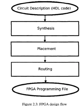
2.3.1 FPGA Design Flow
CAD tools are an essential part of circuit design targeting FPGA platforms. CAD tools are used to convert the user's specification of the digital circuit (i.e., source code describing the circuit's functionality) into a logic netlist during synthesis that can be later downloaded and programmed onto the FPGA fabric. Recent CAD tools can be used to optimize the circuit for area, speed or power consumption to meet design requirements. Figure 2.3 shows the typical steps in the design flow used by CAD tools to map the design specification into a netlist downloadable onto an FPGA [24].
Input into a CAD tool is a source code that describes the functionality of the circuit at the Register Transfer Level (RTL description). The source code is usually written using a hardware description language such as Verilog or VHDL. The synthesis process converts the source code into a netlist of basic logic gates that implement the functionality of the circuit. The netlist can then be optimized using suitable algorithms to meet design requirements.
Synthesis
Placement
Routing
1 _
Programming FileFigure 2.3: FPGA design flow
direct influence on the amount and complexity of routing performed in the next step, and as a result, placement directly influences the critical path delay of the implemented circuit. Once placement is performed, a routing algorithm is used to interconnect the placed logic blocks. The routing process is even more important than placement because of the effect it has on the critical path delay of the circuit. Routing in FPGA's consumes most of the chip area, and it's attributed for most of the circuit delay [24].
The output from the routing process is a bit stream stored in a programming file that's used to specify the state of every programmable element inside the FPGA. The entire design flow process, including synthesis, placement and routing, is referred to as design
compilation or just synthesis (not to be confused with the synthesis step from the design
flow). The next section will discuss the CAD tool and the FPGA device used in this research.
2.4 Stratix FPGA Device and the Quartus II CAD Tool
The Altera Stratix EP1S40F780C5 FPGA device was the chosen to be the target FPGA device in this research [25]. Logic blocks within the Stratix family of FPGA's are referred to as logic elements (LE's) in the Stratix documentation [25].
In addition to logic elements, Stratix FPGA devices contain DSP blocks (used for dedicated multiplication), phase-locked loops (PLL's), and memory blocks. Stratix devices have three different sizes of memory blocks: M512 (512 bits), M4K (4096 bits), and Mega-RAM (65,536 bytes). The blocks with the fastest speed are the M512, followed by the M4K followed by Mega-RAM. Stratix devices have anywhere between 920,448 and 7,427,520 on-chip memory bits.
Quartus II version 7.2 [28] is the CAD tool used in this research. It is provided by Altera Corporation to provide the necessary tools for circuit designs targeting Altera FPGA's. Quartus II includes a library of parameterizable megafunctions (LPM functions), which implement some standard building blocks commonly used by digital circuit designers. Megafunctions are often implemented more efficiently in the target FPGA than the custom design, although this is not always the case [28].
2.5 Design Space Exploration (DSE)
The design space of a digital embedded system is the complete set of all possible hardware system design configurations that can be used to achieve the system's functionality. Since embedded systems are required to perform an increasing number of tasks, the complexity of embedded systems is increasing; embedded systems are becoming more parameterized and taking on more system parameters especially with the development of FPGA platforms. Thus, the design space of embedded systems is getting extremely large (i.e., the number of possible hardware configurations that can perform a system's functionality is increasing).
Every configuration within the design space has a set of K objectives, and K objective functions, Fk(pO, where pi represents the parameters of the system and k € {1, 2, ..., K}.
Objective functions are used to measure how well a configuration from the design space meets the objectives of maximizing performance, minimizing chip area, reducing power consumption, etc. However, not all of the configurations in a design space are optimal. In fact, the majority of configurations within a design space are sub-optimal for any given application. Therefore, it's crucial that embedded system designers isolate and identify optimal configurations from a design space, since they play a key role in maximizing the system's performance and reducing its cost. This is the main objective of design space exploration.
2.5.1 Multi-objective Optimization
Embedded system designers are usually concerned with balancing a set of competing
objectives. Most often, these objectives include maximizing the system's processing speed
In multi-objective optimization problems there is not one single optimal configuration, but rather a set of optimal configurations known as the Pareto-optimal set. A configuration becomes part of the Pareto-optimal set if one objective cannot be improved without sacrificing another.
Embedded system designers explore the design spaces of their systems to approximate the Pareto-optimal set by eliminating all sub-optimal configurations. Unlike the design space, the Pareto-optimal set is limited in size, allowing designers to choose a suitable configuration for their system from a small and finite set of configurations.
2.5.2 DSE of Parameterized Cores
Embedded system designers explore the design spaces of their parameterized cores in search of a hardware platform configuration suitable for their applications. This suitable configuration is often required to balance between each of the objectives without violating any of the requirements. As the complexity of embedded systems increases, their design spaces expand. Soon, it becomes impractical to evaluate every possible configuration in the design space to come up with a suitable platform configuration, as concluded by Givargis et al [29]. Therefore, the process of DSE needs to be automated; to this end many approaches have been proposed including the use of genetic-based algorithms. A good summary of the proposed approaches can be found in the literature [10, 30, 31].
For this thesis work, a genetic-based algorithm was chosen to automate the DSE process as will be detailed in the following sections.
Genetic-based Algorithms Approach
The concept of genetic-based algorithms, also known as evolutionary algorithms, was developed in 1975 by Holland [32]. It proved to be effective in solving multi-objective optimization problems, like the one we face in the DSE process of parameterized soft-core processors.
members of a population survive and reproduce, while weak members are eliminated. Many versions of genetic algorithms have been proposed; a summary of genetic algorithms for multi-objective optimization is given in the literature [33, 34].
The genetic algorithm chosen in this research was the Simple Evolutionary Algorithm for Multi-objective Optimization (SEAMO), proposed by Valenzuela [13]. It accepts a set of design configurations, generated by the user, as input. This set has a fixed size N; the set is referred to as a population. Each member of the population is known as a chromosome. In our case, a chromosome represents a unique design configuration. A chromosome is composed of a collection of genes; in our case, a gene represents a parameter of the system. Each parameter (i.e., gene) can be assigned a value from a finite set of possible values that the parameter can take.
After receiving the input initial population, each chromosome gets evaluated separately in terms of its objectives, which are the FPGA area utilization and critical path delay in our research. The algorithm runs for a number of iterations; an iteration is referred to as a generation. During each iteration, chromosomes within a population are randomly grouped into pairs (i.e., parents); each pair is allowed to reproduce to generate an offspring chromosome. Two operators control the operation of the genetic algorithm: the crossover and the mutation operators.
During reproduction, genes from both parents are combined to generate an offspring chromosome according to the crossover genetic operator. A cut-point is selected randomly by the crossover operator, and the left half of one parent in the pair is combined with the right half of the other parent. The crossover operator is only applied a certain percentage of the time; this percentage is specified by the crossover rate, rc. Next, a certain percentage of
the offspring is mutated; this percentage is specified by the mutation rate, rm. Offspring
At the end of each generation the performance of offspring chromosomes gets evaluated in terms of their objectives. If an offspring chromosome performs better than its parent chromosomes, the offspring chromosome replaces one of the parent chromosomes selected at random. Otherwise, the offspring chromosome is discarded.
The genetic algorithm is allowed to run for a number of generations, G, at the end of which the final population converges toward an optimal configuration set, the Pareto-optimal set. The SEAMO algorithm has four parameters: the crossover rate (rc), the
mutation rate (rm), the population size (N) and the number of generations (G).
I. Anderson et al. [35] conducted a case study involving a parameterized Altera Nios soft-core processor to approximate its Pareto-optimal set of design configurations. The SEAMO genetic algorithm was employed to perform an automatic exploration of the processor's design space. It was concluded that the SEAMO algorithm proved to be useful in providing a good approximation of the Pareto-optimal set of design configurations, from which designers can easily choose a suitable hardware platform design for their application.
2.6 Closely Related Work
P. Yiannacouras [8, 36, 37] developed a CAD, tool named SPREE (Soft Processor Rapid Exploration Environment) that was used to automatically generate soft-core processors targeted for implementation on FPGA platforms, and explore their design spaces. SPREE has two main modules, an RTL generator and a library that stores the hardware modules used to build his soft-core processor. The RTL generator is responsible for instantiating the necessary hardware component modules from the library to build a datapath according to an input description of the architecture. The RTL generator also generates the necessary control logic.
tradeoffs of various functional unit implementations (shifters and multipliers) and different pipeline depths, along with other architectural optimizations. He determined that customizing processors with the recommended features showed an improvement in performance-per-area over general purpose processors.
The main difference between this work and the SPREE system is the exploration procedure used. The SPREE system utilizes a manual design space exploration approach, where the user is to use SPREE to generate different architectural variations of the soft-core in order to compare the various design tradeoffs. On the other hand, this work uses an automatic design space exploration approach, based on a genetic algorithm, to explore the design space of the target soft-core.
B. Fort et al. [39] developed a 4-way interleaved multithreaded soft-core processor that's instruction-set compatible with Altera's Nios II soft-core processor. The authors compared the area and performance of the multithreaded soft-core processor versus two chip multiprocessors (CMP) systems, one of which is developed using Altera's Nios II soft-core processor. They concluded that using multithreaded processors in FPGA environments can result in significant area savings with comparable performance to a CMP system. This work differs from Fort's in that our processor does not support multithreading capabilities; Fort's work does not include an automatic scheme for the design space exploration.
The PEAS-III system [41] developed by M. Itoh followed a hardware software co-design approach that is capable of generating synthesizable RTL descriptions of pipelined processors. He developed pre-designed stage models of each pipeline stage and stored them in a library. The PEAS-III system generates the datapath of the processor core by instantiating the stage models from the library, and then cascading them in series. It enables a wide range of explorations, but in order to make a small architectural change, significant changes to its description are required.
Changing the multiply/divide unit to sequential was explored, and a multiply-accumulate (MAC) instruction was added. Several processor cores were developed using the PEAS-III system and then evaluated, including a MIPS R3000 processor, a DLX processor [42], and a simple RISC controller. In the results, area and clock speed as reported by the synthesis tool were compared. However, the PEAS-III system does not support automatic design space exploration of soft-core processors, which is what distinguishes it from this work.
It was concluded from experimental results that using this tool, designers can make intelligent decisions regarding the assignment of values to the parameters of an embedded hardware platform. SCBuild was designed to be general enough to accept any parameterized soft-core given, provided that the user supplies a template description of the core that follows proper syntax. The initial version of SCBuild, developed by I. Anderson, supports a simple RISC processor CPU design. The work in this thesis is an extension of the work initiated by I. Anderson to enable SCBuild to support and explore the design space of a widely deployed commercial soft-core processor, Altera's Nios II.
2.7 Summary
Chapter 3
UW_Nios II
The parameterized UW_Nios II processor developed in this research is our own implementation of the Nios II standard core. UW_Nios II resembles Altera's Nios II soft-core processor and supports the same instruction set. It was developed to enable us to use it with the SCBuild CAD tool to perform DSE of Nios II processor. We now present a description of its key features.
3.1 Instruction Set
The UW_Nios II core supports the same instruction set as Altera's Nios II cores [18]. It supports three types of instruction word formats: I-type, R-type, and J-type.
3.1.1 I-Type Instructions
The main characteristic of the I-type instruction-word format is that it contains an immediate value embedded within the instruction word. I-type instructions are composed of three components:
o A 6-bit opcode field (OP)
o Two 5-bit register fields (A, B)
o A 16-bit immediate field (IMM16)
31 30 29 28 27 26 25 24 23 22 21 20 19 18 17 18 15 14 13 12 11 10 9 8 7 6 5 4 3 2 1 0
A B IMM16 OP
Figure 3.1:1-type instruction format
3.1.2 R-type Instructions
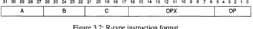
In R-type instruction-word formats all arguments and results are specified as registers. R-type instructions are made up of 3 components:
o A 6-bit opcode field (OP)
o Three 5-bit register fields (A, B, C)
o An 11-bit opcode-extension field (OPX)
In the majority of cases, fields A and B specify the sources operands. The destination register is specified within field C. Certain R-type instructions have a small immediate value embedded in the low-order bits of the OPX field. Figure 3.2 illustrates the format of R-type instructions.
31 30 29 28 27 26 25 24 23 22 21 20 19 18 17 16 15 14 13 12 11 10 9 8 7 6 5 4 3 2 1 0
A B G OPX OP
Figure 3.2: R-type instruction format
3.1.3 J-type Instructions
J-type instructions have two components: o A 6-bit opcode field (OP)
o A 26-bit immediate data field (IMM26)
The only J-type instruction is the "call" instruction. Figure 3.3 illustrates the format of J-type instructions.
31 30 29 28 27 26 25 24 23 22 21 20 19 18 17 18 15 14 13 12 11 10 9 8 7 6
IMMED26
s * % 3 2 1 0
OP
The UW_Nios II core supports an instruction set with a total of 94 instructions including data transfer instructions, arithmetic and logical instructions, move instructions, comparison instructions, shift and rotate instructions, program control instructions, along with other control instructions. The OP field in the instruction word specifies the class of an opcode. The majority of the OP field values are for I-type instructions. For the single J-type instruction OP = 0x00. OP = 0x3a is used for all R-type instructions, in which case, the OPX field differentiates the instructions.
3.2 Structure
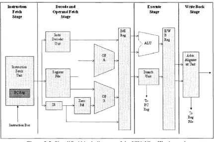
Figure 3.4 shows the design hierarchy of the UW_Nios II core. The UW_Nios II core has two main modules, the datapath and the control unit. The datapath is further divided into 4 main components: the Instruction Fetch Stage (IF), the Decode and Operand Fetch Stage (DOF), the Execute Stage (EX) and the Write Back Stage (WB).
^
•i
Datapath
\l
Execute_Stage
*
1 nstruction_Fetch_Stage
UW_Nios_ll
s
* •
Control Unit
Write_Back_Stage
'
DecodejDperand_Fetch_Stage
Figure 3.4: UW_Nios II Design Hierarchy
soft-core processors are optimal in terms of area and performance [8]. As a result, the UW_Nios II core was designed to be a four-stage pipelined RISC processor core.
In the first pipeline stage, the Instruction Fetch Stage (IF), instructions are fetched from the instruction memory. They are later decoded and operands are fetched from the Register File during the second stage, the Decode and Operand Fetch Stage (DOF). The Program Counter is incremented in this stage. The operands are then passed on to the third stage, the Execute Stage (EX), where instructions are executed by the ALU. Branch and Jump instructions are resolved in this stage and the Control Registers are read or written if necessary. Finally, the result is written back to either the register file or the data memory during the last pipeline stage, the Write Back Stage (WB). Figure 3.5 shows a simplified block diagram of the UW_Nios IFs datapath core illustrating the four pipeline stages.
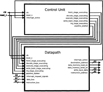
Figure 3.5: Simplified block diagram of the UW_Nios IFs datapath
the Decode_Operand_Fetch_Stage and Execute_Stage are stored in the pipeline registers D/E and E/WB, respectively.
elk . reset
n-M ir!tenrept„«cttve
Control Unit
reset n
fetch j*ts»g«_exe«tirif
execute_stag«ja>Eecuting writej£iackjtage„e*ecutirt5i Sr^st»gejsxeeutiM}
I I I I I I H
32
3 2 .
elk resetjs
fetchjstagejsxetutlrwf dftcode^stage^executirw)
nwitejjack^stage^exeaftlng Ir$js6a§*j**«£utlftg pipellnej&alled
intemiptjre*ju«stjsl$nate datajfcus
instruction bus
Datapath
lnterruptm#aitfc
desJasi8ti<wi_address dattjwecnoiyj'ead^en data_memofy_wiifce_efl
•wrSteJbackjdata Instruction address
-M-Figure 3.6: UW_Nios II block diagram with interfaces
memory word in the data memory; it's used for store operations. A 1-bit write-enable, "data_memory_write_en", and a 1-bit read-enable, "data_memory_read_en", signals are also produced by the datapath and supplied to the data memory to control the flow of information to and from the data memory module. The "write_back_data" output signal is used to transfer a 32-bit word to the data memory for store operations. Finally, the instruction memory receives a 32-bit "instruction_address" signal from the datapath; it contains the address of the instruction to be fetched.
The current version of the UW_Nios II core does not contain additional hardware for handling data and control hazards in the pipeline. Therefore, hazards must be handled in software by inserting NOPs in between instructions in a program.
Variants of the UW_Nios II core were generated and compiled using Altera's Quartus II design software version 7.2. In order to test the functionality of different variants to ensure that they functioned as expected, a number of instructions and operands were applied to the inputs of different variants of the core and the outputs were observed using the Quartus II's Simulator Tool [28]. In this way, the processor's instructions were verified to be functioning correctly.
3.2.1 Datapath
Data processing operations performed by the processor are handled by the datapath module. Figure 3.6 is a simplified block diagram representation of the datapath module. The four major components of the datapath are the Instruction Fetch Stage, the Decode and Operand Fetch Stage, the Execute Stage and the Write Back Stage.
The Execute Stage module contains the arithmetic and logic unit (ALU), the branch unit, the control registers and the EX/WB pipeline registers. The ALU module contains the logic necessary to perform arithmetic, logical and shift operations on data stored in the register file. The ALU can be configured with or without hardware multiplication using the
Include Multiplier parameter. The Include Divider parameter is used to either emulate
division operations in software or implement them in hardware.
The shifter unit module can be configured to optionally handle the arithmetic, logical, shift and rotate operations. The Arithmetic Shifter Implementation, Logical Shifter
Implementation and Rotator Implementation parameters control which shifters are
included for the shifter unit module, and whether their implementations will be "basic" or "barrel".
The write back stage module controls whether data is written back to the register file or to the data memory. In the case of memory access instructions, the write back stage module performs the necessary alignment of the memory addresses and the data to be written back to the data memory, and generates the necessary enable signals. Figure 3.7 shows a more detailed block diagram illustrating the inputs and outputs of each pipeline stage in the datapath module.
3.2.2 Control Unit
The control unit controls the flow of information within the datapath module and the transition between the pipeline stages. In other words, the control unit determines when the pipeline stalls, and when to transfer the execution of an instruction from one pipeline stage to the next. The control unit is also responsible for taking the appropriate action in case the "reset" signal or any of the external interrupt signals are triggered.
3.3 Parameters
logical shifter and a rotator. The user is given the option of removing or including any or all of these types of shifters. Each of these shifter types can be emulated in software (pi = 1; p2 = 1; p3 = 1), implemented in hardware as a "basic" shifter causing a one-bit-per-clock-cycle shift, or as a "barrel" shifter allowing shifting of multiple bit positions in a single clock cycle. The core can have either a signed or unsigned hardware multiplier module. If no multiplier implementation is chosen, multiplication will be emulated in software (an exception will be triggered upon a multiplication instruction). The multiplier can be implemented using logic element (LE's) resources within the FPGA or, to achieve a better performance, the multiplier can be implemented using dedicated DSP multiplication blocks. The ALU can be configured with or without a hardware divider module using either the Include Signed Divider parameter or the Include Unsigned Divide parameter. In case no hardware division is picked, division operations will be emulated in software (an exception will be triggered upon a division operation). The designer can choose to implement the instruction decoder, register file and pipeline registers using LE's or, if LE resources are more critical, they can be implemented using dedicated memory blocks. The output from the instruction decoder is a set of control signals that make up the control word, which will later be used to define the operations that need to be performed to implement the decoded instruction.
3.4 Comparison of UW_Nios II and Altera Nios II
After the design of the UW_Nios II was complete, it was necessary to see how well its variants performed when compared with Altera's Nios II variant cores. This section presents the results of comparison between the UW_Nios II variants against Altera's Nios II variant cores. Note that each variant is obtained using a specific set of parameter values.
3.4.1 FPGA Device and CAD Tools
performing our FPGA-based exploration. The targeted device is Altera's Stratix EP1S40F780C5 FPGA device [25], which is a mid-sized device in the Stratix family with
Table 3.1: UW_Nios II Processor Hardware Parameters
I'arameter
Arithmetic Shifter Implementation (pi) Logical Shifter Implementation
(p2)
Rotator Implementation (p3) Include Signed Multiplier (p4)
Include Unsigned Multiplier (p5)
Include Unsigned Divider (p6) Include Signed Divider (p7)
Instruction Decoder Implementation (p8) Register File Implementation
(p9) Pipeline Register Implementation (plO)
Possible Values
(1) None, (2) Basic, (3) Barrel
(1) None, (2) Basic, (3) Barrel
(1) None, (2) Basic, (3) Barrel
(1) No (i.e., emulated in SW), (2) Using LE's & area optimization, (3) LE's & speed optimization, (4) Using
DSP blocks
(1) No (i.e., emulated in SW), (2) Using LE's, (3) Using DSP blocks
(1) No (i.e., emulated in SW), (2) Using LE's (1) No (i.e., emulated in SW), (2) Using LE's (1) Using LE's, (2) Using RAM memory blocks
(1) Using LE's, (2) Using Memory blocks
(1) Using LE's, (2) Using Memory blocks
the fastest speed grade. It has a total LE capacity of 41,250 LE's, a total of 3,423,744 RAM memory bits, and a total of 14 DSP blocks. In addition, Altera's Quartus II v7.2 [28] CAD software was used for the synthesis, technology mapping, placement and routing of all designs to the targeted FPGA device.
3.4.2 Metrics for Evaluating Soft-core Processors
In order to measure the speed performance and area utilization of the different variants of the UW_Nios II soft-core processor, an appropriate set of measurement metrics is required. For an FPGA device, area utilization is measured by counting the number of equivalent resources consumed. In the Stratix family of FPGAs, the main resource is the Logic Element (LE), where a LE is composed of a 4-input lookup table (LUT) and a flip flop. Thus, area is given in terms of the equivalent number of LEs consumed.
For now, speed performance is measured in terms of the maximum clock frequency (in Mhz) achieved by the processor (based on the critical path delay), as reported by Quartus IPs Timing Analyzer Tool, after placement and routing.
3.4.3 Comparison with Altera's Nios II Cores
To ensure that our comparisons with Altera's Nios II cores were as fair as possible, several measures were taken. Comparison with the Nios II Economy core was omitted because it is an un-pipelined soft-core processor while the UW_Nios II is a four stage pipelined core. Thus comparison is performed against the Standard and the Fast cores only. Each of the two Nios II cores was generated with memory systems identical to those used in our designs: two 8KB blocks of RAM for separate instruction and data memory. Caches were not accounted for in our measurements, though extra logic to support the caches will inevitably count towards the Nios II areas. Nios II cores support operating systems (OS) instructions, which are not yet supported by the UW_Nios II variants. Despite the previously mentioned differences, we still believe that comparisons between Altera's Nios II cores and the UW_Nios II variants are fair.
within 7% of Altera's Standard Core. In this core, the register file was implemented using dedicated on-chip RAM memory blocks and the pipeline registers were implemented using logic elements. And when a similar UW_Nios II core was synthesized with an area optimization option, up to a 47% saving in area compared to Altera's Standard core was achieved. This large saving in area was countered by a 60% drop in clock frequency. In this core, the register file and the pipeline registers were both implemented using on-chip RAM memory blocks. Table 3.2 illustrates these results along with other similar results.
Table 3.2: Comparison with Altera's Nios II Standard Core
Shifters .Serial Serial Serial Serial Serial Serial Multiplier/ Divider Software Emulation Software Emulation Software Emulation Software Emulation Software Emulation Software Emulation Instruction Decoder Impl. LE-based RAM-based RAM-based LE-based RAM-based LE-based Register File Impl. RAM-based RAM-based RAM-based RAM-based RAM-based RAM-based Pipeline Register Impl. LE-based LE-based RAM-based RAM-based LE-based LE-based Optim. Option Speed Speed Area Area Area Area Clk (Mhz) 205 176.41 90.01 78.21 109.68 98.9 Eq. LE's 935 875 677 729 738 800 % Decrease in freq. 7.6 20.5 60 65 51 55 % Reduction
in LE usage
27.5 32.1 47 43 42 38
was synthesized with an area optimization option, up to a 30% saving in area compared to Altera's Standard core was achieved. This saving in area was countered by a 59% drop in clock frequency. In this core, the register file and the pipeline registers were both implemented using on-chip RAM memory blocks. Table 3.3 illustrates these results along with other similar results.
Table 3.3: Comparison with Altera's Nios II Fast Core
Shifters Barrel Barrel Barrel Barrel Barrel Barrel Multiplier/ Divider DSP blocks DSP blocks DSP blocks DSP blocks DSP blocks DSP blocks Instruction Decoder Impl. LE-based RAM-based RAM-based LE-based RAM-based LE-based Register File Impl. RAM-based RAM-based RAM-based RAM-based RAM-based RAM-based Pipeline Register Impl. LE-based LE-based RAM-based RAM-based LE-based LE-based Optim. Option Speed Speed Area Area Area Area Clk (Mhz) 125 123.53 82.3 89 113.62 104.53 Eq. LE's 1554 1445 1202 1249 1273 1320 % Decrease in freq. 37.5 38.2 59 55 43 48 % Reduction inLE usage 9.4 15.7 30 27 25 23
Bearing in mind the design differences between Altera's Nios II cores and our UW_Nios II variants, it is not our goal to draw architectural conclusions from comparisons with Altera's cores, since we do not have access to Altera's Nios II architectures. The main reason for presenting performance comparisons between Altera' cores and our variants is to show that our design is relatively competitive when compared with commercial, hand-optimized soft-core processors.
3.4.4 Hardware vs. Software Multiplication Support
uses a software multiplication routine in which hardware performs a portion of the multiplication operation. This multiplier is much faster than the typical software version, which uses a series of shift and add operations. In this work, we do not consider such hybrid implementations; instead we focus only on either full or no hardware multiplication support.
New FPGAs have dedicated on-chip DSP blocks that are capable of supporting full hardware multiplications. We conducted an experiment on our UW_Nios II to compare its performance when hardware multiplication was implemented using the DSP blocks one time, and using logic elements (LEs) the second time. As shown in Figures 3.8 and 3.9, in the case of LE-based hardware multiplication, the UW_Nios II core used 37% more area, and had a clock frequency that was 43% slower than a similar core with DSP-based hardware multiplication. From this experiment, we conclude that DSP-based hardware multipliers are a better choice than the LE-based version.
Research conducted by Yiannacouras et al [37] showed similar results. They generated different variations of a RISC soft-core processor that supports a MIPS I instruction set architecture (ISA). Some of those variants supported full hardware multiplication and in the rest, multiplication was emulated in software. A set of benchmark circuits were run on their variants and their performance was compared. In terms of the number of cycles required to execute the benchmark circuits, it was found that some applications were minimally sped up while others benefited up to 8X from a hardware multiplier. Thus it was concluded that multiplication support is an application-specific design decision. In general, especially for multiply-intensive applications, hardware multiplication consumes more area but provides better processing performance.
3.4.5 Register File Implementation
UW Nios II Area
5000
_« 4000
UJ
""! 3000
a-01 2000
o
* 1000
11 - SW Emulation 2 - LE-based HW Multiplication 3 - DSP-based HW Multiplication
Configuration
Figure 3.8: UW_Nios II Area
UW Nios II Clock Period
20 n
S 15-t
o
fc 10
Q.
u
o 5 H 0
11 - SW Emulation 2 - LE-based HW Multiplication 3 - DSP-based HW Multiplication
Configuration
Figure 3.9: UW_Nios II Clock Period
B 1 - LE-based Register File 2 - RAM-based Register File
Figure 3.10: Clock Period for Register File Implementation
UW_Nios_ll-Area
2900 -• n in t&nxm m 2400
o 1900
-LLI
li: 1400
-o
* 900
-S i Rsra
4 U U r i
1 2
Configuration
B 1 - LE-based Register File
2 - RAM-based Register File
Figure 3.11: LE Utilization for Register File Implementation
When the register file is implemented using LE's, a large area is consumed because one lookup table (LUT) is required to store 1 bit (a LUT is composed of a 4-input lookup table and a flip flop). Therefore, a 32-bit register requires at least 32 LUT's to implement it. The reason for the significant rise in clock frequency (in the cased of a RAM-based register file over the LE-based version) is that the RAM blocks are optimized memory components, and thus access times are shorter. Also, the LE's used to implement the register file (in an LE-based register file) could be scattered throughout the FPGA fabric after placement, thus complicating routing process and resulting in longer routes. This in turn increases the critical path delay and translates into a smaller clock frequency. From this experiment, we conclude that RAM-based register files are a better choice than the LE-based version.
(0
c^ "O
o
I-<u
O.
J *
u
o o
1 0 -T
9
8
/ 6
-O -f
UW Nios II Clock Per
1 2
3.4.6 Pipeline Register Implementation
Finally, an experiment was conducted to study the impact of pipeline register implementation on the overall performance of the processor. Figures 3.12 and 3.13 illustrate that impact on the processor's clock period and equivalent area respectively. In this experiment, two similar UW_Nios II variants were compared; in the first variant the pipeline registers were implemented using logic elements (LE's) and, in the second one, they were implemented using RAM memory blocks.
It was found that the first variant had a clock frequency was about 27% larger than the second variant, but it consumed 55 more LE's. This increase in area is relatively small compared to the gain achieved for the clock frequency. This increase in clock frequency can be attributed to the fact that using LE's to implement pipeline register allows them to be placed closer to the logic of the next stage, resulting in shorter routes. That in turn translates into a shorter critical path delay resulting in a shorter clock period (i.e., higher clock frequency). From this experiment, we conclude that LE-based pipeline registers are a better choice than the RAM-based version.
>d
(ns
)
•£
a.
Cloc
k
UW_Nios_ll Clock Period
C
D
O
1 1
8 7 6
-m 1 - LE-based Pipeline
Registers
2 - RAM-based Pipeline Registers
1 2 Configuration
![Figure 2.2: Simplified illustration of a Logic Element (LE) [53]](https://thumb-us.123doks.com/thumbv2/123dok_us/1465902.1179619/30.615.126.525.175.375/figure-simplified-illustration-logic-element-le.webp)