ISSN(Online): 2319-8753 ISSN (Print): 2347-6710
I
nternational
J
ournal of
I
nnovative
R
esearch in
S
cience,
E
ngineering and
T
echnology
(A High Impact Factor, Monthly, Peer Reviewed Journal) Visit: www.ijirset.com
Vol. 8, Issue 5, May 2019
Design and Implementation of Arithmetic and
Logical Block Using QCA Technology
S.Gladson #1, K.Srirevathi *2
Associate Professor, Department of ECE, Sasurie College of Engineering, Vijayamangalam, Tirupur,
Tamilnadu, India#1
II-M.E-VLSI Design, Department of ECE, Sasurie College of Engineering, Vijayamangalam, Tirupur,
Tamilnadu, India*2
ABSTRACT: In this paper an eight bit arithmetic and logical block is designed using QCA technology. QCA cells does not conducts the information as current as used in conventional logic circuits. It operates based on the concept of Columbic Interaction of the states of electrons in QCA cells. Quantum dot cellular automata (QCA) is one of the emerging technologies that shows features to overcome the limitations like high computation throughput and power consumption faced in CMOS technologies. A lot of research has been done in designing universal logic gates, combinational circuits, sequential circuits and ALU using QCA and has shown its efficiency due to its small size and high computational speed. Apart from these advantages of QCA, it also has a great potential for low power consumption. So far, the research in QCA circuit design was mainly based on irreversible circuits and as proved by Landauer in, that any circuits designed using traditional logic gates will inevitably loss information in the form of energy dissipation in a circuit. So, designing of eight bit ALU block at low power can be achieved by using QCA technology.
I. INTRODUCTION
Quantum dot cellular automata (QCA) is one of the emerging technologies that shows features to overcome the limitations like high computation throughput and power consumption faced in CMOS technologies. A lot of research has been done in designing universal logic gates, combinational circuits, sequential circuits and ALU using QCA and has shown its efficiency due to its small size and high computational speed. Apart from these advantages of QCA, it also has a great potential for low power consumption. So far, the research in QCA circuit design was mainly based on irreversible circuits and as proved by Landauer in, that any circuits designed using traditional logic gates will inevitably loss information in the form of energy dissipation in a circuit.
Traditional logic functions such as AND, OR etc., are not reversible in nature as more than one input are mapped into one output state. But in reversible logic the logic functions have one to one correspondence between inputs and output, i.e., there is a distinct output assignment for each distinct input. Therefore, input can be distinctly determined from its output in reversible logic and hence no loss of information occurs in circuits designed using reversible logic.
Like all other emerging nanotechnologies such as quantum computing, optical computing, Spintronic, DNA computing, molecular computing etc., QCA also has applications of reversible logic. Reversible logic is proposed to maintain the trend according to Moore’s Law and to minimize the energy dissipation occurring during computation. It is shown that information loss occurring in terms of energy dissipation while computing in traditional logic circuits would not occur if it is carried out in a reversible way.
ISSN(Online): 2319-8753 ISSN (Print): 2347-6710
I
nternational
J
ournal of
I
nnovative
R
esearch in
S
cience,
E
ngineering and
T
echnology
(A High Impact Factor, Monthly, Peer Reviewed Journal) Visit: www.ijirset.com
Vol. 8, Issue 5, May 2019
submicron to deep submicron and to manometer regime over last five decades. But the scaling of CMOS devices at nano scale affects the performance of several factors like heat dissipation and leakage currents. The heat generated can no longer dissipate and results in damage of the chip as more and more devices are packed into the same area. So many novel technologies and materials have been extensively researched and developed at nano scale to replace conventional transistor based VLSI technology.
Among several other alternatives, Quantum Dot Cellular Automata (QCA) is a revolutionary promising transistor less quantum paradigm that performs computation and routing information at nano domain. The unique feature of QCA is that logic states are represented by a cell. A cell is a nano scale device capable of transferring data by two state electron configurations. The advantages of QCA over conventional CMOS technology include lesser delay, high density circuits and low power consumption which permits us to perform quantum computing in near future.
QCA is an evolving nanotechnology and has capability to develop digital circuits with higher packaging density, reduced area, much lower power dissipation, and higher switching speed. QCA results in ultra-dense, high-performance digital devices as it works at nanometre scale. It is used to design new logic circuits which are basically a translation of standard logic devices. Dimensional scaling of CMOS based logic circuits is approaching its limit of feature size reduction. Further reducing the size of CMOS based circuits result in many problems and doesn’t produce the necessary output required.
It is believed that the physical size and the corresponding performance of the various circuits based on CMOS technology is close to the reaching limit. Alternatives to conventional CMOS technology is QCA which provides higher density, lower dissipation of power, higher clock frequency and better output results are needed. Quantum Dot Cellular Automata (QCA) technology is explored and introduced. When a new technology is introduced, new design principles are also necessary to consider. The design nature of QCA is not very complicated, instead it is simple than the conventional technologies.
II. LITERATURE SURVEY
This paper proposes a detailed design analysis of sequential circuits for quantum-dot cellular automata (QCA). This analysis encompasses flip-flop (FF) devices as well as circuits. Initially, a novel RS-type FF amenable to a QCA implementation is proposed. An algorithm for assigning appropriate clocking zones to a QCA sequential circuit is implemented. A technique referred to as stretching is used in the algorithm to ensure timing and delay matching. This algorithm relies on a topological sorting and enumeration step to consistently traversing only once the edges of the graph representation of the QCA sequential circuit.
QCA is a novel technology which provides implementation of digital circuits in nanoscale. QCA circuits work in higher speed, smaller size and less power consumption compared to conventional CMOS circuits. In this paper, a new design for T flip flop (T-FF), by using of special feature of QCA circuits capabilities, is proposed. This T-FF has additional inputs that can be used better in sequential circuits as memory elements. These inputs can reset and preset T-FF and no more cells needed to add them to the designed circuit. Proposed T-T-FF is simulated using the QCA Designer and simulation results prove its validity.
ISSN(Online): 2319-8753 ISSN (Print): 2347-6710
I
nternational
J
ournal of
I
nnovative
R
esearch in
S
cience,
E
ngineering and
T
echnology
(A High Impact Factor, Monthly, Peer Reviewed Journal) Visit: www.ijirset.com
Vol. 8, Issue 5, May 2019
A novel fault-tolerant full-adder for quantum dot cellular automata is presented. Quantum-dot cellular automata (QCA) are an emerging technology and a possible alternative for semiconductor transistor based technologies. A novel fault-tolerant full-adder is proposed in this paper: This component is suitable for designing fault-fault-tolerant QCA circuits. The redundant version of full-adder is simple in structure and more robust than the standard style for this device. By considering two-dimensional arrays of QCA cells, fault tolerance properties of such block full-adder can be analyzed in terms of misalignment, missing and dislocation cells. In order to verify the functionality of the proposed device, some physical proofs are provided. The results confirm our claims and its usefulness in designing digital circuits.
In modern era, Quantum-Dot Cellular Automata (QCA) is most promising and emerging technology to implement the digital logic circuit at nanoscale. Due to inherent unique characteristics of QCA, it can be possible to have device that can functions consuming high density, ultra low power and very fast clocking speeds. This work displayed an optimized design and implementation of basic flip-flops like RS, JK, D and T in QCA. The functionality and correctness of proposed flip flop circuits is verified by comparing the QCA Designer generated simulation result with truth table of proposed circuits. For general purpose nano processor, the proposed circuit can be used as basic building block.
III. METHODS
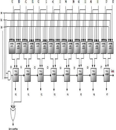
The Arithmetic Logic Unit (ALU) performs the basic arithmetic and logical operation and consists of arithmetic extender, logical extender and one bit full adder as shown in figure 4.1.Three control signals determine the operation of the ALU. M is the mode control variable used to select between arithmetic and logical operations. S1 and S0 are used in combination with M to select between the eight arithmetic and logical operation the ALU supports.
Fig 1.Architecture of ALU
Arithmetic Extender
The Arithmetic extender modifies the second operand and passes it to the Full adder to the arithmetic. According to truth table we write Boolean equation of arithmetic extender shown in equation (1) and design logic circuit of arithmetic extender shown in fig. 6.
= 1’ + 0’ … (1)
Logical Extender
ISSN(Online): 2319-8753 ISSN (Print): 2347-6710
I
nternational
J
ournal of
I
nnovative
R
esearch in
S
cience,
E
ngineering and
T
echnology
(A High Impact Factor, Monthly, Peer Reviewed Journal) Visit: www.ijirset.com
Vol. 8, Issue 5, May 2019
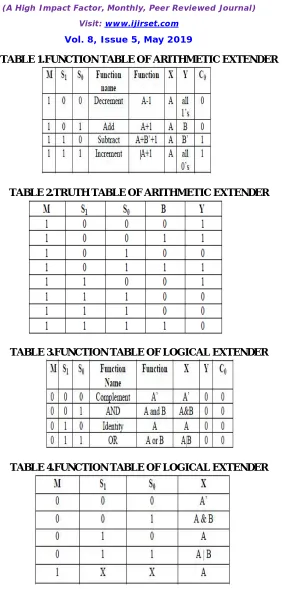
TABLE 1.FUNCTION TABLE OF ARITHMETIC EXTENDER
TABLE 2.TRUTH TABLE OF ARITHMETIC EXTENDER
TABLE 3.FUNCTION TABLE OF LOGICAL EXTENDER
TABLE 4.FUNCTION TABLE OF LOGICAL EXTENDER
ISSN(Online): 2319-8753 ISSN (Print): 2347-6710
I
nternational
J
ournal of
I
nnovative
R
esearch in
S
cience,
E
ngineering and
T
echnology
(A High Impact Factor, Monthly, Peer Reviewed Journal) Visit: www.ijirset.com
Vol. 8, Issue 5, May 2019
X = M’S1’So’+ M’S1So + SoAB + S1A +MA ……..(2)
(a) (b)
Fig 2.(a)Logic circuit of Arithmetic Extender (b) Logic circuit of Logical Extender
Full Adder
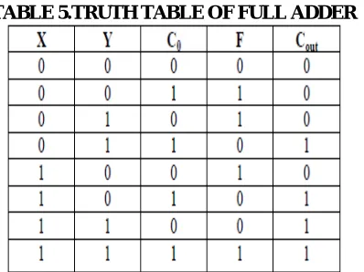
Full adder performs the addition of three bits. In full adder, we have given three inputs X, Y and C0,
where C0 is carry in signals shown in equation (3).
0 = 1 . . . (3)
TABLE 5.TRUTH TABLE OF FULL ADDER
The Boolean equations for Full adder are shown in equations (4) & (5) and logic circuit of full adder as shown in figure 4.3.
ISSN(Online): 2319-8753 ISSN (Print): 2347-6710
I
nternational
J
ournal of
I
nnovative
R
esearch in
S
cience,
E
ngineering and
T
echnology
(A High Impact Factor, Monthly, Peer Reviewed Journal) Visit: www.ijirset.com
Vol. 8, Issue 5, May 2019
Fig .3.Logic Circuit for Full Adder
Fig. 4.Logic Circuit for 8-bit ALU Fig. 5.Implementation of ALU Block in QCA Designer Tool
ISSN(Online): 2319-8753 ISSN (Print): 2347-6710
I
nternational
J
ournal of
I
nnovative
R
esearch in
S
cience,
E
ngineering and
T
echnology
(A High Impact Factor, Monthly, Peer Reviewed Journal) Visit: www.ijirset.com
Vol. 8, Issue 5, May 2019
V. IMPLEMENTATION AND RESULTS
5.1 AND GATE:
Fig.6. Implementation of QCA AND Gate, Output waveform for QCA AND Gate
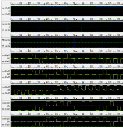
Fig 7. Output waveform for 8-bit ALU
VI. CONCLUSION
ISSN(Online): 2319-8753 ISSN (Print): 2347-6710
I
nternational
J
ournal of
I
nnovative
R
esearch in
S
cience,
E
ngineering and
T
echnology
(A High Impact Factor, Monthly, Peer Reviewed Journal) Visit: www.ijirset.com
Vol. 8, Issue 5, May 2019
REFERENCES
1. Companio R, L. Molenkamp and D.J. Paul, Technology Roadmap for Nanoelectronics, 2000.
2. Craig S. Lent andBeth Isaksen, “Clocked molecular quantum-dot cellular automata”, IEEE Transaction on Electron Devices 50(9), 1890-1896, 2003.
3. Huang J, M. Momenzadeh, F. Lombardi, “Design of sequential circuits by quantum-dot cellular automata”, Microelectronics Journals. 38, 525– 537, 2007.
4. Lent, Craig S., and P. Douglas Tougaw. "Lines of interacting quantum‐ dot cells: A binary wire", Journal of applied Physics 74, no. 10: 6227-6233, 1993.
5. Lent C. S., and P. D. Tougaw, “A device architecture for computing with quantum dots”, Proceedings of the IEEE, Vol. 85, No. 4, pp. 541- 557, 1997.
6. Orlov A.O., I. Amlani, G.H. Bernstein, C.S. Lent, G.L. Snider, “Realization of a Functional Cell for Quantum-Dot Cellular Automata”, Science, Vol 277, pp 928-930, 1997.
7. Orlov A.O., I. Amlani, C. S. Lent, G. H. Bernstein, and G. L. Snider, “Experimental demonstration of a binary wire for quantum-dot cellular automata”, Appl. Phys. Lett., vol. 74, pp. 2875–2877, 1999.
8. Ottavi M, V. Vankamamidi, F. Lombardi, Clocking and cell placement for QCA, in: Proceedings of the IEEE Nanotechnology Conference, pp 343– 346, 2006.
9. Srivastava S ; S. Sarkar ; S. Bhanja, “Power Dissipation Bounds and Models for Quantum-dot Cellular Automata Circuits”, 2006. IEEE-NANO,Sixth IEEE Conference on Nanotechnology, 2006.
10. Tougaw P. D., C. S. Lent, “Logical devices implemented using quantum cellular automata”. Journal of Applied Physics75 (3):1818–1825, Year 1994.
11. Timler J., and C.S. Lent, “Power gain and dissipation in Quantum-dot Cellular Automata”, Journal of Applied Physics, Vol. 91, No. 2, pp. 823- 831, 2002.