Implementation of Low Power Single-Ended
8T SRAM using AVLG Technique
Sonal Verma 1, Ravi Tiwari 2
M. Tech Scholar, Department of Electronics and Telecommunication Engineering, Shri Shankaracharya Technical
Campus, Bhilai, Chhattisgarh, India1
Assistant Professor, Department of Electronics and Telecommunication Engineering, Shri Shankaracharya Technical
Campus, Bhilai, Chhattisgarh, India2
ABSTRACT: Recently, there is an increase in demand for ultra-low power dissipation battery-operated devices. The battery operated devices to utilize the battery for longer duration needs ultra-low power consuming circuits to utilize the battery for longer duration. SRAMs are widely used for mobile & computer applications as both on chip and off-chip memories, because of their availability and low standby leakage. SRAM has been under its renovation stage recently, aiming to withstand the ever-increasing process variation as well as to support ultra-low-power applications using even ultra-low voltages. This paper presents a single-ended with dynamic feedback control 8T Static RAM using Adoptive Voltage Level Ground (AVLG) technique. The 1-kB 8T SRAM array is designed in 65nm BSIM4 CMOS process technology at 300mv with reduced power consumption.
KEYWORDS: Single ended 8T Static RAM, AVLG, reduced power consumption, ultra-low voltages.
I. INTRODUCTION
The portable devices such as hand held mobile devices and personal digital assistants are gaining more popularity as well as making changes in every aspect of our daily lives. The major concern enhancing the demand for portable device market is multimedia data processing, which includes the image/video applications. Video applications require a large amount of embedded memory access, which results in significant power consumption and thus limits the battery life time. Power dissipation has turned into a vital thought due to the increased integration and operating speeds, as well as due to the explosive growth of battery operated appliances. The power consumption can be minimized by using non-conventional device structures, new circuit topologies and optimizing the various architectures. The portable micro-processor controlled devices contain embedded memory which represents an extensive part of the system on chip (SoC). Ultra-low power on chip memory is now mandatory to achieve higher reliability and longer battery life for handheld devices. POWER dissipation has become a most important design constraint, as we know the utilization wall, and the low power circuit architecture, and system level techniques are sought out.
Likewise, the Static Random Access Memory (SRAM) is the most important digital macro and its segment on a system-on-chip (SoC) is consistently increasing. Decreasing the power dissipation of SRAM will not only decrease the overall system power dissipation, but will also build the yield and enhance the SoC reliability. Despite the fact that the six transistor (6T) SRAM cell is a generally used standard in industry, it has its own limitations as it has conflicting read and write requirements.
II. RELATED WORK
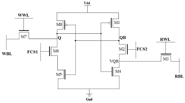
The single-ended design is used to reduce the differential switching of power during read and write operations. The SE-DFC enables writing through single nMOS in 8T and it also separates the read and write path. 8T consists of 8 transistors from which there are two cross coupled inverters (M8-M6-M5, M1-M2-M4) to retain the written data during hold mode. Two feedback NMOS transistors (M6/M2) are connected between pull-up PMOS transistors (M8/M1) and pull-down NMOS transistors (M5/M4). One NMOS access transistor (M7) connects true storage node Q to the write bit line (WBL) when the write word line is at VDD. One NMOS pass gate transistor (M3) connects virtual complementary storage node QB to the read bit line (RBL) when the read word line is at VDD. Two separate feedback control signals FCS1and FCS2 control M6 and M2 respectively. Another separate read word line (RWL) signal controls M3. A single ended with dynamic feedback control (SE-DFC) 8T SRAM Cell is shown in Fig.1.
Fig.1: Proposed 8T SRAM Cell
A. Write Operation
The feedback cutting scheme is used to write into 8T SRAM Cell. In this scheme, during write 1 operation FCS1 is made low which switches OFF M6 i.e. no current flow. When the RWL is made low (M3 OFF) and FCS2 high, M2 conducts connecting Complementary Q (QB) to the ground. Now, if the data applied to word bit line (WBL) is 1 and WWL is activated (M7 ON) (Table 1), then current flows from WBL to Q and creates a voltage hike on Q via M7-writing 1 into the cell. Moreover, when Q changes its state from 0 to 1, the inverter (M1– M2–M4) changes the state of QB from 1 to 0 because M1 is OFF. Now, to write a 0 at Q, WWL is made high (M7 ON), FCS2 low (M2 OFF) and WBL is pulled to the ground. The low going FCS2 leaves QB floating, which can go to a small negative value, and then the current from pull-up pMOS M1 charges QB to 1.
B. Read Operation
TABLE 1
Operation Table of 8T SRAM Cell
Hold Read Write ‘1’ Write ‘0’
WWL ‘0’ ‘0’ ‘1’ ‘1’
RWL ‘0’ ‘1’ ‘0’ ‘0’
FCS1 ‘1’ ‘0’ ‘0’ ‘1’
FCS2 ‘1’ ‘0’ ‘1’ ‘0’
WBL ‘1’ ‘0’ ‘1’ ‘0’
RBL ‘1’ Discharge ‘1’ ‘1’
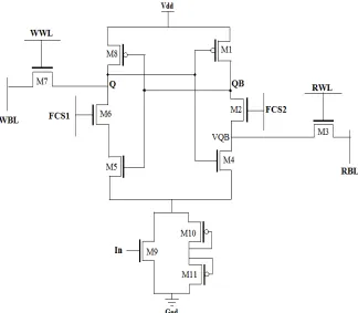
In memory cells power is the main constraint. So, that to overcome the high power consumption, AVLG circuit is connected to 8T SRAM cell circuit. The AVLG circuit is connected in between pull-down network and ground. This consists of 2 pMOS and 1 nMOS, which are connected in parallel. By adding that circuit we can reduce decrease the power consumption. It would lift the ground potential of the circuit to decrease the power consumption of the 8T SRAM Cell circuit. Depending upon the input the output also varied and the usage of clock is to prevent any defect in 8T SRAM cell function during power consumption. Fig.2 shows the schematic of 8T SRAM using Adoptive Voltage Level Ground (AVLG) technique.
III.EXPERIMENTAL RESULTS
Here we are presenting the simulated result implemented in Tanner 16.0 EDA tool. We have implemented and simulated the design of 8T SRAM Cell using Adoptive Voltage Level Ground (AVLG) technique in T-Spice to analyse the power consumption and to carry out the waveform for Write and Read operations. The proposed 8T is implemented in a 64 × 16 bit SRAM array in 65-nm Bulk CMOS BSIM4 technology. The 1-kb SRAM comprises of four banks and each bank consists of 16 words ×16 bits. The circuit is simulated with the supply voltage of 300mV at 25°C.
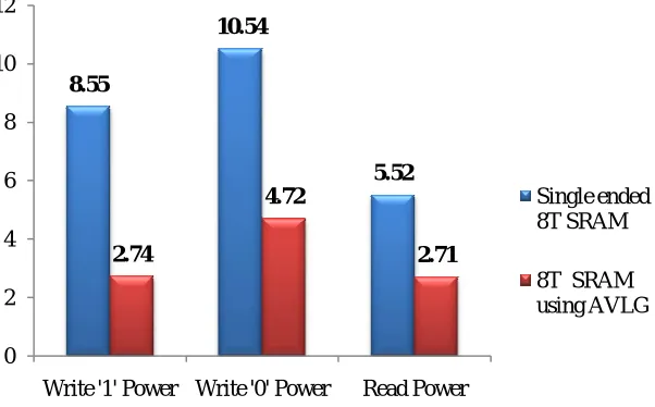
Table 2 gives the average power consumption of Write ‘1’, Write ‘0’ and Read operations of 1-kb array of Single ended 8T SRAM and 8T SRAM using AVLG technique at 300 mV supply with 65nm BSIM4 CMOS Technology.
TABLE 2
Comparison of Power Consumption of 1-kB Array of 8T SRAM
Write ‘1’ Power Write ‘0’ Power Read Power
Single ended 8T SRAM
8.55μW 10.54 μW 5.52 μW
8T SRAM using AVLG
2.74 μW 4.72 μW 2.71 μW
Fig.3 gives the comparisons of average power consumption of Write ‘1’, Write ‘0’ and Read operations of 1-kb array of Single ended 8T SRAM and 8T SRAM using AVLG technique at 300 mV supply.
Fig.3: Power consumption of Single ended 8T SRAM and 8T SRAM using AVLG 8.55 10.54 5.52 2.74 4.72 2.71 0 2 4 6 8 10 12
Write '1' Power Write '0' Power Read Power
Single ended 8T SRAM
Figure.4: (a),(b) and (c) below represents the simulation waveform for Write ‘1’, Write ‘0’ and Read operations respectively of 8T SRAM using AVLG Technique.
Fig.4 (a): Simulation Waveform for Write ‘1’ Operation
Fig.4 (c): Simulation Waveform for Read Operation
IV.CONCLUSIONS
We have designed and implemented 8T SRAM Cell using Adoptive Voltage Level Ground (AVLG) technique in Tanner 16.0 Tool. The circuit is being simulated and verified in T-Spice software and the result has given us the reduced power consumption. It can be operated at ULV of 200-400 mV power supplies. The advantage of decrease in power consumption of the proposed 8T SRAM Cell enables it to be worked for battery operated SoC design.
REFERENCES
[1] C. B. Kushwah and S. K. Vishvakarma, “A Single-Ended With Dynamic Feedback Control 8T Sub-threshold SRAM Cell” in Proc, IEEE Trans. Solid-State Circuits, vol. 24, no. 1, pp. 373-377, Jan. 2016.
[2] Ravi Tiwari and Khemraj Deshmukh, “Design and Analysis of Low-Power 11- Transistor Full Adder” in IJAREEIE, Vol. 3, Issue 6, pp. 10301-10307, June 2014.
[3] C. B. Kushwah and S. K. Vishvakarma, “A sub-threshold eight transistor (8T) SRAM cell design for stability improvement,” in Proc. IEEE Int. Conf. IC Design Technol. (ICICDT), pp. 1–4, May 2014
[4] C. B. Kushwah, S. K. Vishvakarma, and D. Dwivedi, “Single-ended sub-threshold FinFET 7T SRAM cell without boosted supply,” in Proc. IEEE Int. Conf. IC Design Technol. (ICICDT), pp. 1–4, May 2014.
[5] M.-H. Tu et al., “A single-ended disturb-free 9T sub-threshold SRAM with cross-point data-aware write word-line structure, negative bit-line, and adaptive read operation timing tracing,” IEEE J. Solid-State Circuits, vol. 47, no. 6, pp. 1469–1482, Jun. 2012.
[6] C.-H. Lo and S.-Y. Huang, “P-P-N based 10T SRAM cell for low leakage and resilient sub-threshold operation,” IEEE J. Solid-State Circuits, vol. 46, no. 3, pp. 695–704, Mar. 2011.
[7] S. A. Tawfik and V. Kursun, “Low power and robust 7T dual-Vt SRAM circuit,” in Proc. IEEE Int. Symp. Circuits Syst., pp. 1452–1455, May 2008.
[8] N. Verma and A. P. Chandrakasan, “A 256 kb 65 nm 8T sub-threshold SRAM employing sense-amplifier redundancy,” IEEE J. Solid-State Circuits, vol. 43, no. 1, pp. 141–149, Jan. 2008.
[9] B. H. Calhoun and A. P. Chandrakasan, “A 256-kb 65-nm sub-threshold SRAM design for ultra-low-voltage operation,” IEEE J. Solid-State Circuits, vol. 42, no. 3, pp. 680–688, Mar. 2007.