Early Tag Access to Improve the Reliability of
the Cache Memory
Suvitha S1, Murugan T2
P.G. Student, Department of Electronics Engineering, Adhiyamann College of Engineering , Hosur , Tamilnadu, India1
Assistant Professor, Department of Electronics Engineering, Adhiyamann College of Engineering , Hosur , Tamilnadu,
India2
ABSTRACT: Due to increasing concern about various transient errors, processors adopt error protection mechanisms for their on-chip components. Caches are the largest structure in current microprocessor. Tag bits in the cache memories are also exposed to transient errors. To prevent transient errors and to improve the energy efficiency of data caches in embedded processors, we propose a new cache design technique, referred to as early tag access (ETA) cache is designed. Before the actual cache access it determine the destination way of memory instruction. If a hit occurs during the ETA , it thus, enables only the destination way to be accessed. Compared with the existing cache design techniques, the ETA cache reduces the unnecessary way access and improve energy efficiency.
KEY WORDS: Early Tag Access , Tag Bits , Cache Memory
I. INTRODUCTION
Due to the continued technology scaling to the nanometer regime, computer systems are becoming vulnerable to transient errors. So it is important to Prevent errors and provide correction mechanism for cache memories. Tag bits in cache memories cause transient errors and to reduce their vulnerability few efforts have been made. Considerable efforts have been made to reduce vulnerability of data bits, but errors in tag bits are also critical for data integrity. For example, transient errors in tag bits can incur false misses in dirty cache lines, and consequently, stale data can be consumed. However, a complex protection mechanism for tag bits can degrade performance due to their long latency. Clearly, providing high reliability with a low-cost mechanism to tag bits is necessary to guarantee system integrity and maintain system performance.
Due to the spatial locality of programs, there are many tag bits whose values are the same with those of other tag bits in adjacent cache sets. In other words, when a cache line is accessed or replaced, another cache line whose tag bits are the same with those of the accessed cache line is very likely to be found in an adjacent cache set. This phenomenon is called tag bits similarity in this paper. We exploit the tag bits similarity to improve reliability of tag bits against transient errors. When an error is detected by the conventional parity check bits, the error can be corrected if the same tag bits are present in an adjacent cache set. Faulty tag bits are simply replaced with intact tag bits from the adjacent cache set.
In this paper we propose a new cache design technique known as ETA cache to improve the energy efficiency of data caches in the processor. It determines the destination way of memory instruction.
II. BACKGROUND AND RELATED WORK
the word cannot be corrected. By adding more check bits to the word, more powerful detection and correction codes can be created. The number of check bits required is a function of the size of the data to be protected. Single error correct/double error detects (SEC-DED) codes were also used.
In Cache Replication is another method. The basic idea of ICR is to replicate frequently accessed cache lines into other cache lines, which are predicted not to be accessed further, called dead blocks. Spaces of the dead blocks in the L1 data cache are recycled to maintain duplicates of frequently used data bits against transient errors. To avoid significant performance degradation by dead block miss
predictions, ICR uses a prediction strategy. This scheme can be applied to protect tag bits because replicated locations are calculated by fixed formulation and replicated cache lines can be used to correct tag bits errors in the active lines. However, the dead block prediction technique is based on a prediction, and thus ICR can increase cache miss rates and the number of write-backs resulting in large performance loss and energy consumption increase
A technique to detect the false miss in highly associative cache with CAM basedtag. The technique involves subdividing the tags and providing backup
checking for cases the tags are partially matched. An original tag encoding scheme is proposed to reduce the frequency of back-up checking. Modifications to support the technique do not increase the cache access latency. The performance degradation incurred by additional cycles for false miss checking is very low. A tag is divided into two parts which contain respectively the high and low order bits. The part containing the low order bits is used as first subtag. The second sub-tagis produced by XORing the two parts. Since the diversity of the high order bits of the tags is low, by XORing the two parts together, we essentially impose the diversity of the loworder bits to the high order bits. The frequency of close hits therefore is expected to be reduced. The encoding scheme does not lose the tag data
information. The high order bits of a tag can be reproduced by XORing the two sub-tags stored in the sub-CAMs. This technique can be applied only to CAM-based highly associative caches. Furthermore, only pseudomiss can be detected and additional cycles are needed for pseudomiss checking.
III. PROPOSED SYSTEM
In the proposed system a dedicated encoder decoder based memory access system is developed where the memory concept is implemented, in the proposed design we used ML comparison keyword based search method which reduces even more sensing delay.
To improve the energy efficiency of data caches in embedded processors a new cache design technique, referred to as ETA cache is designed. Before the actual cache accesses technique performs to determine the destination ways of memory instructions. If a hit occurs during the Tag Access it thus, enables only the destination way to be accessed .
A. Design and analysis of cell:
The cell is sensing element in this design. The input data address is given as an input to the cell through the search line and by using the comparison circuit in the cell it compares directly with every bit of the storage word.
B. Design and analysis of a matrix using cell:
The cell designed in the previous module is ordered in a form of matrices as an eight bit word. The 8×8 matrix has the binary data as the bit stored in the cell. The compare operation of the memory provides this module output as a matrix.
C. Design and analysis of a encoder matrix:
The modules 3 have the encoder, in the evolution stage it senses the binary data of the address from the matrix of the tag line and provide the encoded output from this module. The matrix is compared in the pre-stored state and given as a output matrix.
D. Design and analysis of a integrator:
The output from the previous module is 8×8 matrix which is not in a single binary search data form. Hence the integrator is used in this module to combine the data to form an 8 bit binary data output. The output is generated as a integrator output.
We introduce a versatile auxiliary bit to boost the search speed of the Memory. This newly introduced auxiliary bit is similar to the existing Pre-computation schemes but it has a different operating principle. We first briefly discuss the Pre-computation schemes before presenting our proposed auxiliary bit scheme.
Pre-Computation Memory Design:
The pre-computation Memory uses additional bits to filter some mismatched words. From the data bits these extra bits are derived and are used as the first comparison stage. For example, number of “1” in the stored words are counted and kept in the Counting bits segment. When a search operation starts, number of “1”s in the search word is counted and stored to the segment on the left. These extra information are compared first and only those that have the same number of “1”s (e.g., the second and the fourth) are turned on in the second sensing stage for further comparison. Significant amount of power required for data comparison is reduced, statistically. To reduce energy consumption the main design idea is to use additional silicon area and search delay.
The previously mentioned pre-computation and all other existing designs shares one similar property. Between the matched ML and the 1-mismatch ML the ML sense amplifier essentially has to distinguish. This makes Memory designs sooner or later face challenges since the driving strength of the single turned-on path is getting weaker after each process generation while the leakage is getting stronger. This problem is usually referred to as Ion/Ioff . Thus, we propose a new auxiliary bit that can concurrently boost the sensing speed of the ML and at the same time improve the Ion/Ioff of the Memory by two times.
Parity Bit Based Memory:
The parity bit based Memory design consisting of the original data segment and an extra one-bit segment, derived from the actual data bits. We only obtain the parity bit, i.e., odd or even number of “1”s.
The obtained(fig) parity bit is placed directly to the corresponding word and ML. Thus the new architecture has the same interface as the conventional Memory with one extra bit. During the search operation, there is only one single stage as in conventional Memory. Hence, the use of this parity bits does not improve the power performance.
STEPS INVOLVED IN PROPOSED SYSTEM
Initialize memory,
Extract counting of 1’s,
Extract parity bit,
Detect ML sensing line.
In our proposed technique, we implement new form of Memory architecture to reduce the existing drawbacks. First check the parity bit for input data and content in memory in searching the data in cache memory. To form as an index for fetching data we count number of ones in parity bit data. Then this was given to RAM memory to renaming or update the data.
STEP 1: Initialize memory
The memory architecture is initialized and it gives condition to ML Sensing line to detect power level.
Data and Address is initialized.
STEP 2: Extract counting of 1’s
The number of “1” in the stored words and number of 1’s in the data bits are also counted and both are compared and finally search was done for matched no. of ones.
Counted no. of ones will form index for extracting parity bit.
STEP 3: Extract parity bit
The parity bit is mainly extracted to increase the searching process for Memory.
The parity bit for the stored words and parity bit for the input data are extracted and kept in parity bit segment.
The extracted parity bits are compared, checked and the corresponding match line are selected. If it is not matched a miss will occur.
STEP 4: Detect ML sensing line
The matching line in the register is extracted and it also controls each ML sensing lines.
These ML sensing lines consists of controlling block at each output. This method will mainly use to select the exact match line for given input bit data.
Finally, the searched address and page information in memory are updated.
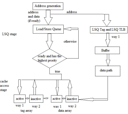
Load/store queue operation
Fig Operation of a load/store instruction under the proposed ETA cache.
IV. SIMULATION RESULT
XILINX ISE is a software tool produced by Xilinx for synthesis and analysis of HDL designs , enabling the developer to synthesize their designs, perform timing analysis examine RTL diagrams, simulate a design reaction to different stimuli and configured the target devices.
The memory architecture is initialized and it gives condition to ML Sensing line to detect power level and searched address and data is found with low energy consumption.
V. CONCLUSION
This paper presented a new energy-efficient cache design techniques for low-power embedded processors. At the early LSQ stage with partial tag comparison the proposed technique predicts the destination way of a memory instruction. During the cache access stage if the prediction is correct only one way needed to be accessed, thereby reducing the energy consumption significantly and improve performance. Future work is being directed toward extending this technique to other levels of the cache hierarchy and to deal with multithreaded workloads.
REFERENCES
[1] Intel XScale Microarchitecture, Intel, Santa Clara, CA, USA, 2001.
[2] C. Zhang, F. Vahid, and W. Najjar “A highly-configurable cache architecture for embedded systems,” in Proc. 30th Annu. Int. Symp. Comput. Archit., Jun. 2003, pp. 136–146.
[3] S. Segars, “Low power design techniques for microprocessors,” in Proc. Int. Solid-State Circuits Conf. Tuts., Feb. 2001.
[4] S. Manne, A. Klauser, and D. Grunwald, “Pipline gating: Spculation conrol for energy reduction,” in Proc. Int. Symp. Comput. Archit., Jun.–Jul. 1998, pp. 132–141.
[5] M. Gowan, L. Biro, and D. Jackson, “Power considerations in the design of the alpha 21264 microprocessor,” in Proc. Design Autom. Conf., Jun. 1998, pp. 726–731.
[6] A. Malik, B. Moyer, and D. Cermak, “A Low power unified cache architecture providing power and performance flexibility,” in Proc. Int. Symp. Low Power Electron. Design, 2000, pp. 241–243.
[7] T. Lyon, E. Delano, C. McNairy, and D. Mulla, “Data Cache Design Considerations for the Itanium Processor,” in Proc. IEEE Int. Conf. Comput. Design, VLSI Comput. Process., 2002, pp. 356–362.
[8] D. Nicolaescu, A. Veidenbaum, and A. Nicolau, “Reducing power consumption for high-associativity data caches in embedded processors,” in Proc. Design, Autom., Test Eur. Conf. Exhibit., Dec. 2003, pp. 1064–1068.
[9] C. Zhang, F. Vahid, Y. Jun, and W. Najjar, “A way-halting cache for low-energy high-performance systems,” in Proc. Int. Symp. Low Power Electron. Design, Aug. 2004, pp. 126–131.
[10] J. Montanaro, R. T. Witek, K. Anne, A. J. Black, E. M. Cooper, D. W. Dobberpuhl, P. M. Donahue, J. Eno, W. Hoeppner, D. Kruckemyer, T. H. Lee, P. C. M. Lin, L. Madden, D. Murray, M. H. Pearce, S. Santhanam, K. J. Snyder, R. Stehpany, and S. C. Thierauf, “A 160-MHz 32-b 0.5- W CMOS RISC microprocessor,” IEEE J. Solid-State Circuits, vol. 31, no. 11, pp. 1703–1714, Nov. 1996.