Available online: https://edupediapublications.org/journals/index.php/IJR/ P a g e | 3844
An Effective Redix-2 FFT Processor Based On Parallel
Processing of Input Data Streams
Y. Varsha, MS.P.Rajeshwari, Mr.B.Sivakumar,
PG Scholar, Assistant Professor, Professor & HOD, Department of Electronics and Communication Engineering,
Ellenki Institute of Engineering and Technology, Patelguda, Patancheru, Medak (Dist), Telangana, India
Abstract—Nowadays, many applications require
simultaneouscomputation of multiple independent fast Fourier transform (FFT) operations with their outputs in natural order. Therefore, this brief presents a novel pipelined FFT processor for the FFT computation of two independent data streams. The proposed architecture is based on the multipath delay commutator FFT architecture. It has an N/2-point decimation in time FFT and an N/2-point decimation in frequency FFT to process the odd and even samples of two data streams separately. The main feature of the architecture is that the bit reversal operation is performed by the architecture itself, so the outputs are generated in normal order without any dedicated bit reversal circuit. The bit reversal operation is performed by the shift registers in the FFT architecture by interleaving the data. Therefore, the proposed architecture requires a lower number of registers and has high throughput.
Keywords— Bit reversal, bit reversed order, fast Fouriertransform (FFT), multipath delay commutator (MDC) FFT, normal order.
I.INTRODUCTION
Fast Fourier transform (FFT) is one of the most commonly used operations in the wireless communication applications, such as orthogonal frequency division multiple (OFDM) accesses, ultra wide-band, digital video
broadcast terrestrial, and signal processing application as well. A family of pipelined FFT architectures is discussed in which single-path delay feedback (SDF) and multipath delay commutator (MDC) are very popular. There are applications, such as image processing, array signal processing, multiple-input–multiple-output OFDM, and so on, in which more than one data stream need to be processed. Therefore, simultaneous multiple FFT operations are required and a dedicated bit reversal circuit is also required to generate the outputs in natural order.
Available online: https://edupediapublications.org/journals/index.php/IJR/ P a g e | 3845
complexity is N . These circuits are suitable for bit reversing the data from the pipelined FFT architecture. However, only the bit reversal structures are proposed. The bit reversal circuit is integrated to FFT architecture; as a result, the total register requirement of the design is reduced from 5N/2 to 2N . Two-, four-, and eight-parallel pipelined radix-2k decimation in frequency (DIF) feed forward FFT architectures are proposed and they need extra N registers to generate the output in natural order. Moreover, these two-, four-, and eight-parallel FFT architectures can start its operation only when x(n+N/2), x (n+3N /4), and x (n+7N /8)samples arrive, respectively. Therefore,hardware is underutilized and additional registers are required to store the first N/2, 3N/4, and 7N/8 samples. Modified MDC FFT architectures with a new data scheduling method and a rearranging structure are proposed in which the drawbacks of [10] are eliminated. The architectures operated at the frequency of incoming sample rate but the architecture operates half the clock frequency to generate the same Thus, the throughput of the architecture is doubled, if all the architectures are operated at the same speed. Similarly, a combined single path delay commutator SDF FFT architecture with I/O in natural order is proposed in which the bit reversal is carried out only with N/2 registers. However, its throughput is low and the required number of register is high. Low complexity FFT architectures are proposed but these architectures can process only real-valued signals (signals only with real part). Moreover, they generate two outputs per clock cycle and these outputs are not in natural order. Thus, most of the recent architectures require bit reversal structures to generate the outputs in natural order.The proposed architecture is designed to process two independent data streams simultaneously with less amount of hardware. The odd inputs, which are in natural order, are first bit reversed and then they are processed by N/
2-point decimation in time (DIT) FFT. The even samples are directly processed by N/2-point DIF FFT, so its outputs are in bit reversed order. Therefore, the outputs of N/ 2-point DIF FFT are bit reversed. The outputs of the two
N/2-point FFTs are further processed by the two-parallel butterflies to generate the outputs of N -point FFT in natural order. The bit reversing is carried out by thescheduling registers, which are actually used to delay the samples for performing the butterfly operations. Thus, the FFT architecture does not use any dedicated circuit to bit reverse the data. As a result, the proposed architecture requires less number of registers than the prior FFT designs.
II. PROPOSED PIPELINED FFT
ARCHITECTURE
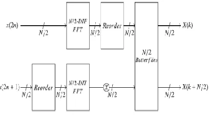
The idea of computing an N -point FFT using two N/ 2-point FFT operations with additional one stage of butterfly operations is
Fig. 1. Idea of the proposed method.
Available online: https://edupediapublications.org/journals/index.php/IJR/ P a g e | 3846
on the results of the two FFTs. Thus, the outputs generated by additional butterfly stage are in natural order.For the purpose of simplicity, the proposed 16-point FFT architecture in Fig. 2 is explained. It has two eight-point MDC FFT architectures to process two data streams. The delay commutator units present at the left side of SW1
dissociate the odd and even samples. The shift registers in the delay commutator units, which receive inputs, are used to bit reverse the odd input samples. These shift registers are called reordering shift registers (RSRs). The RSR in the last stage store outputs from the eight-point DIF FFT and bit reverses them. The BF2 carries out two-parallel butterfly operations between the bit reversed data in the RSR in the last stage and outputs from the eight-point DIT FFT. Thus, the upper and lower BF2 in the last stage generate the FFT outputs of the first and the second data streams in normal order. The two data paths from SW2 are
combined together, so the word length of the data path in last stage is twice and so thick lines are used for representing the data paths and registers.
A. Operation of the Proposed Architecture
The FFT architecture in Fig. 2 is divided into six levels (L1, L2, L3, M1, M2, and M3). The RSR registers in thelevels L1 and M1 reorder the odd input data and the
RSR registers in the levels L3 and M3 reorder the partially
processed even data. The eight-point DIF and DIT FFT operations are performed in the levels L 2and M2,
respectively. The data from L 1and M1can be forwardedto
L2 and M2, respectively, or vice versa with the help of
SW1. Similarly, the data from L2 and M2 can be forwarded
to L3 and M3, respectively, or vice versa with the help of
SW2. SW1 and SW2 have two switches (SW) to swap the
data path and propagate the data to different levels. During the normal mode, the switches (SW1 or SW2) pass the data
at u1, u2, u3, and u4 to v1, v2, v3, and v4, respectively.
However, during the swap mode, the switches (SW1 or
SW2) pass the data at u1, u2, u3, and u4 to v3, v4, v1, and v2,
respectively.SW1 is in the swap mode during the first N/2
clock cycles and it is in the normal mode during N/2 + 1 to
N . On the other hand, SW2 is in the normal mode during
the first N/2 clock cycles and it is in the swap mode during
N/2 + 1 to N . Thus, SW1 and SW2 are in different modes
at any time and change their modes for every N /2 clock cycles. Moreover, if there is transition of data between L
yand Ly+1 or My and My+1 (where y can be 1 or 2), then the
switches (SW1 or SW2) are in the normal mode, and if
there is transition of data between Ly and My+1 or My and Ly+1, then the switches (SW1 or SW2) are in the swap
mode. Like other control signals in the design, the control signals to the switches SW1 and SW2 are externally
provided and these switch control signals swap at every N /2 clock cycles.The two input streams to the FFT processor are represented as X1 and X2. The odd and even
samples of two input streams are disassociated by the delay commutator units in L1 and M1 (X1 is disassociated
into {E1(i,j),O1(i,j)}, respectively, and X2 is disassociated
into {E2(i,j),O2(i,j)}). In these representations, i defines the
nature of the data and j defines the number of thedata set whose FFT has to be computed. The even set of input data [x(0),x(2),x(4) . . .] is defined as E(1,j) and the odd set of input data [x(1),x(3),x(5) . . .] is defined as O(1,j).
E(2,j)/O(2,j) is the set of scheduled or ordered even/odd data, which are ready to be fed to eight-point DIF/DIT FFT. The outputs of eight-point DIF/DIT FFT are defined as E(3,j)/O(3,j), which are fed to the third level for 16-point FFT computation. Table I explains the operation of FFT and the data propagation through different levels.
Available online: https://edupediapublications.org/journals/index.php/IJR/ P a g e | 3847
switch (SW1) is set inthe normal mode and the first eight samples of X2 are loadedinto the registers (4D) in M1. Simultaneously, E1(1, 1) (evensamples of X1) is forwarded from L1 to L2 as E1(2, 1)to perform the eight-point FFT operation. The odd samplesof X1 and X2 are bit reversed by the RSR in L1 and L2,respectively.
2) After eight clock cycles, the positions of the switchesSW1 and SW2 are set in the swap mode and the normal mode,respectively. The odd samples (O1(1, 1)) of
X1 are forwardedfrom L1 to M2 as O1(2, 1) and the even samples (E2(1, 1)) ofX2 is forwarded from M1 to L2 as
E2(2, 1). Simultaneously,E1(2, 1) is forwarded from L2 to
L3 as E1(3, 1) and reorderingis performed.
3) After eight clock cycles, SW1 and SW2 are set in the normalmode and the swap mode, respectively. The odd samples ofX2(O2(1, 1)) are forwarded from M1 to M2 as
O2(2, 1) andO1(2, 1) is forwarded from M2 as O1(3, 1) to
L3 wherethe butterfly operations with E1(3, 1)
corresponding to thelast stage (of the data stream X1) are performed. In themeantime, E2(2, 1) from L2 is forwarded to M3 as E2(3, 1)and reordering is performed in the RSR. 4) After eight clock cycles, the switch (SW2) is set to normalposition to allow the partially processed odd samples (O2(3, 1))from M2 to M3 and perform the butterfly operations of the laststage (of the data stream
X2).Instead of using radix-2 FFTs, as shown in Fig. 2, any higherradix FFTs architecture can be used. In Fig. 3, two radix-23 64-pointFFTs are used to realize 128-point FFT whose multiplier complexity
is 4(log8(N/2) − .5) and working is almost the same as th 16-point FFT. The multiplier complexity of N-point
radix-k FFT algorithm is 4(logk (N/2) − .5).
B. Bit Reversing: The proposed architecture is inspired from the architecture in [7]where N/2 data scheduling registers before the first butterfly unitare used to separate
odd samples from the even samples and delaythem to generate x(n) and x(n + N/2) in parallel. In the proposedarchitecture, this data scheduling registers are reused to bit reverseodd samples. Similarly, N/2 data scheduling registers are used beforethe last butterfly unit to store the partially processed even samplesuntil the arrival of odd samples in [7] and here, these registers arereused to bit reverse the partially processed even samples (outputsfrom DIF FFT). In [8], circuits that use multiplexers and shift registersfor bit reversal are proposed. According to [8], if N is the even powerof r , then the number of registers required to bit reverse N data is(√N −1)2. If N is the odd power of r , then the number of registersrequired to bit reverse N data is (√rN − 1)(√N/r
−1), where r isthe radix of the FFT algorithm. In the proposed architecture, thesebit reversal circuits are incorporated in the data scheduling registerto perform dual role.The RSR used in the 16-point FFT and 64-point FFT architecturesis shown in Fig. 4(a) and (b), respectively. Actually, these structuresare present in the places of the shift registers marked with RSR.Generalized RSR for N -point is shown in Fig. 4(c) in which c0 isN/4−(√N/4−1)2 or N/4−(√(Nr)/4−1)(√N/(4r )−1). Theseregisters in c0 do not involve in reordering. The control signals tothe multiplexer in RSR are properly varied to interleave the data.If log2 N is even, log2 N − 2 multiplexers are required otherwiselog2 N multipliers are required for bit reversal. In the proposed FFT architecture, the first N/4 and the nextN/4 odd input data to DIF FFT are separately bit reversed as theyare required in parallel. Thus, N/ 4-point bit reversing algorithm isenough and the number of registers required to bit reverse N/4 datais either (√N/4 − 1)2 or (√(Nr)/4 − 1)(√N/(4r ) − 1) dependingupon the power of two. In Fig. 2, the RSR (R1–R4) in M1 bitreverses the first N/4 odd input data [x(1), x(3), x(5),
Available online: https://edupediapublications.org/journals/index.php/IJR/ P a g e | 3848 x(7)]. After that, the nextN/4 odd input data [x(9), x(11),
x(13), and x(15)] are bit reversedin R1–R4 [x(9), x(13), x(11), and x(15)], The delay commutator unit in L1 and
M1 feeds the bitreversed odd input samples to u1 and u2, and u3 and u4 (in SW1),respectively. Similarly, in M3, the RSR (R9–R12) bit reverses thefirst N/4 output data [X(0), X(2), X(4), and X(6)] and theRSR (R13–R16) bit reverses the next N/4 output data[X(8), X(10), X(12), and X(14)] of DIT FFT separately, which isexplained in Table III. Thus, the RSR in L3 and M3 bit reverses thepartially processed even data samples from v1 and v2, and v3 andv4 (in SW2), respectively, and feeds to BF2 (via o1 and o2).
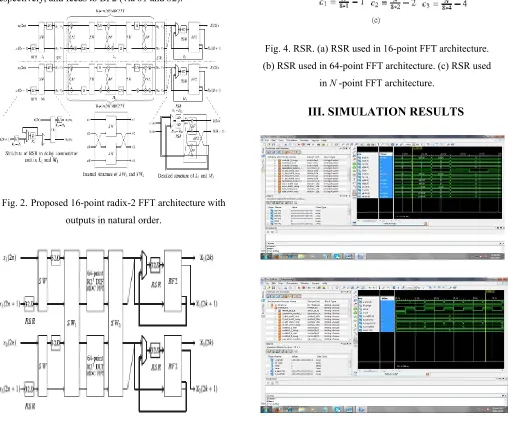
Fig. 2. Proposed 16-point radix-2 FFT architecture with outputs in natural order.
Fig. 3. Proposed 128-point radix-23 FFT architecture.
Fig. 4. RSR. (a) RSR used in 16-point FFT architecture. (b) RSR used in 64-point FFT architecture. (c) RSR used
in N -point FFT architecture.
Available online: https://edupediapublications.org/journals/index.php/IJR/ P a g e | 3849
V. CONCLUSION
This transient has given a unique FFT processor whose outputs area unit generated within the world. The projected method will process 2 freelance information streams at the same time and makes it appropriate for several high-speed periods of time applications.
The bit reversal circuit gift in previous styles is eliminated by integration 2 FFT processors and also the registers, that area unit gift within the design area unit reused for bit reversal. As a result, the necessity of extra registers to bit reverse the outputs is avoided. Moreover, the projected design provides outturn on top of the previous architectures. These attributes create the projected FFT processor superior in sense of hardware quality and performance.
REFERENCES
[1]
Y. Chen, Y.-W. Lin, Y.-C. Tsao, and C.-Y. Lee, “A 2.4-Gsample/s DVFS FFT processor for MIMO OFDM communication systems,” IEEE J. Solid-State Circuits, vol. 43, no. 5, pp. 1260–1273,May 2008. [2] S.-N. Tang, C.-H. Liao, and T.-Y. Chang, “An area-and energy-efficient multimode FFT processor for WPAN/WLAN/WMAN systems,” IEEE J. Solid-State Circuits, vol. 47, no. 6, pp. 1419–1435,Jul. 2012.
[3] P. P. Boopal, M. Garrido, and O. Gustafsson, “A reconfigurable FFT architecture for variable-length and multi-streaming OFDM standards,” in Proc. IEEE ISCAS, May 2013, pp. 2066–2070.
Available online: https://edupediapublications.org/journals/index.php/IJR/ P a g e | 3850 Integr. (VLSI) Syst., vol. 21, no. 4, pp. 720–731,Apr.
2013.
[5] Y.-N. Chang, “An efficient VLSI architecture for normal I/O order pipeline FFT design,” IEEE Trans. Circuits Syst. II, Exp. Briefs, vol. 55, no. 12, pp. 1234–1238, Dec. 2008.
[6] [7] M. Ayinala, M. Brown, and K. K. Parhi, “Pipelined parallel FFT architectures via folding transformation,” IEEE Trans. VeryLarge Scale Integr. (VLSI) Syst., vol. 20, no. 6, pp. 1068–1081,Jun. 2012. [7] M. Garrido, J. Grajal, and O. Gustafsson, “Optimum
circuits for bit reversal,” IEEE Trans. Circuits Syst. II, Exp. Briefs, vol. 58, no. 10, pp. 657–661, Oct. 2011. [8] S.-G. Chen, S.-J. Huang, M. Garrido, and S.-J. Jou,
“Continuous-flow parallel bit-reversal circuit for MDF and MDC FFT architectures,” IEEETrans. Circuits Syst. I, Reg. Papers, vol. 61, no. 10, pp. 2869–2877,Oct. 2014.
[9] M. Garrido, J. Grajal, M. A. Sanchez, and O. Gustafsson, “Pipelined radix-2k feedforward FFT