Chip-Package Co-Design for Optimization of 5.8 GHz LNA
Performance Based on Embedded Inductors
Haiyan Sun1, Wenjun Sun1, Ling Sun1, *, Jicong Zhao1, Yihong Peng2, Jiaen Fang2, Xiaoyong Miao3, and Honghui Wang3
Abstract—This paper presents the design and demonstration of an optimized land grid array (LGA) structure for low noise amplifier (LNA). In order to achieve better circuit performance, the novel chip-package co-design method based on embedded inductors is used. The optimized structure is accurately modeled by ANSYS software. S-parameter is utilized to help in understanding the contributing to the optimized LGA structure. The simulation results for the novel LNA co-design structure show the gain 14.35 dB (>10 dB), input reflection coefficient−15.63 dB (<−10 dB), output reflection coefficient
−24.43 dB (<−10 dB), reverse-isolation −44.7 dB (<−20 dB), and noise figure 2.99 dB (<4 dB), and indicate that the optimized LGA structure based on embedded inductors is fully capable of supporting 5.8 GHz LNA application.
1. INTRODUCTION
With the continuous development of information technology, the demand for low cost and high performance communication systems is increasing. In most RF circuit blocks, low noise amplifiers are usually designed as a single-port circuit for connecting with the band-pass filter or antenna [1, 2]. In order to achieve an efficient input power matching, many on-chip inductors are used in LNA design. These on-chip inductors, implemented in Complementary Metal Oxide Semiconductor transistor (CMOS) technology, not only consume high silicon area, but also have poor electrical performances [3], such as low quality factors. On the other hand, as the operating frequency or bandwidth increases for high data rate, the LNAs become more susceptible to package effects. Those package parasitic effects will cause significant degradation in gain and impedance of LNAs [4]. In previous works, the conventional ceramic quad flat no-lead (QFN) package is usually used for LNA design to satisfy high-performance [5, 6]. The low-pass filter models are used for wire bond packaged LNAs to reveal the package input/output interconnect behave and like an impedance transformer in altering the matching network for optimization design.
In this paper, a chip-package co-design of 5.8 GHz cascade common-source LNA based on embedded inductors is presented. In view of electrical performance design, the matching networks on the package substrate by using embedded inductor are constructed. Designing embedded inductor elements can reduce the number of passive elements and achieve special matching values. In Section 2, a special cascade common-source LNA chip with an on-chip matching network and its performance is discussed in detail. Then, the embedded inductor on the LGA substrate is built and analyzed in Section 3. By taking advantage of the packaging parasitic of bond wire, the LNA co-design architecture is established and optimized in Sections 4–5. Finally, a brief conclusion is given in Section 6.
Received 14 May 2018, Accepted 23 July 2018, Scheduled 30 July 2018 * Corresponding author: Ling Sun ([email protected]).
2. ON-CHIP MATCHED LNA AND ITS PERFORMANCE
2.1. LNA
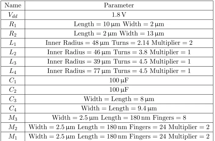
Commercially available CMOS 0.18µm technology, used in this paper, is optimized for high frequency LNA applications. Figure 1 shows the on-chip matched cascode CMOS LNA and its layout. As shown in Figure 1(a), the inductorsL1,L2 and gate-source capacitanceCgs of the transistor M2 are employed for the input matching network, while the inductor L4 and capacitor C4 serve as an output matching network. The LNA is biased to 1.8 V DC voltage and driven from a 50 ohm single ended port. Figure 1(b) shows the layout of the CMOS LNA, where the core part is located in the center, with the large-area matching inductors around the side. Including the bond pads, the die size is 1.13∗1.1 mm2.
Vdd
L1
L2
L3
L4
R1
R2
C1
C2
C3
C4
M1
M2
M3
RFout
RFin
(a) (b)
Figure 1. The cascode CMOS LNA: (a) circuit schematic, (b) layout.
Table 1. LNA circuit parameters.
Name Parameter
Vdd 1.8 V
R1 Length = 10µm Width = 2µm
R2 Length = 2µm Width = 13µm
L1 Inner Radius = 48µm Turns = 2.14 Multiplier = 2
L2 Inner Radius = 46µm Turns = 3.8 Multiplier = 1
L3 Inner Radius = 39µm Turns = 4.5 Multiplier = 1
L4 Inner Radius = 77µm Turns = 4.5 Multiplier = 1
C1 100µF
C2 100µF
C3 Width = Length = 8µm
C4 Width = Length = 9.4µm
M3 Width = 2.5µm Length = 180 nm Fingers = 8
M2 Width = 2.5µm Length = 180 nm Fingers = 24 Multiplier = 2
2.2. LNA Circuit Parameters and Analysis
The parameters of the cascode CMOS LNA in Figure 1 are shown in Table 1. In Linear Network Analysis, the sweep frequency is chosen from 10 MHz to 8 GHz, and the step size is set as 10 MHz. In order to evaluate the design performance, the magnitudes of −10 dB, 10 dB,−20 dB, −10 dB, 4 dB are considered as criterions for the input reflection coefficient S11, gain S21, reverse-isolation S12, output reflection coefficient S22 and noise figure NF, respectively. Figure 2 gives the post-simulation results, which show thatS21,|S12|,S11,S22and NF are 15.29 dB, 31.23 dB,−13.06 dB,−19.76 dB and 3.13 dB. All the results satisfy the design criterions.
Figure 2. On-chip LNA circuit simulation results.
Figure 3. The layout without on-chip inductors.
3. DESIGN AND ANALYSIS EMBEDDED INDUCTOR
3.1. The Layout without Inductors
In order to reduce the silicon area for low cost and perform chip-package co-design, the on-chip input and output matching networks are removed. These matching networks will be designed by using embedded inductor elements on the LGA substrate. Figure 3 shows the unmatched LNA layout, and the die size is reduced from 1.13∗1.1 mm2 to 0.497∗0.473 mm2. Compared with the structure shown in Figure 1(b), the area is reduced by 81%.
3.2. Stand-Alone Inductor Structure
The inductors can be generally divided into surface mount technology (SMT) inductor, embedded inductor and bond-wire inductor. The embedded inductor is preferred over the other types of inductors because of its high integration and ease of customizing special inductance values [7]. In this paper, the structure of embedded inductor is shown in Figure 4, which has the simplicity of configuration. In this structure, the magnetic field generated by adjacent lines changes the current distribution of the wire. If spaces between traces are reduced, the magnetic field will be stronger, and the current density in the metal lines will be more asymmetric.
Figure 4. Structure of square spiral inductor.
Table 2. Parameters of embedded inductor.
Name Parameter
w 50µm
s 30µm
din 90µm
n 3
dout 510µm
davg 300µm
The formula that is valid for planar spiral integrated inductors can be defined as [8]:
L=K1μ0 n 2davg
1 +K2ρ
(1)
where davg is the average diameter, davg = 0.5(din+dout), and the fill ratio ρ is given by the formula
ρ= (dout−din)/(dout+din). The coefficients K1 andK2 are 2.34 and 2.75 [9, 10]. According to Table 2 and Equation (1), the calculated value of embedded inductor is 2.7143 nH.
(a) (b)
3.3. Modeling and Comparison with Field Solvers
To compare with calculated value, the scattering parameter (S) and admittance matrix (Y) can be obtained by ANSYS HFSS. By matrixY, the inductance (L) andQ-factor (Q) can be obtained according to Equations (2) and (3), respectively.
L = im
1
Y11
2πf (2)
Q = abs
⎛
⎝im
1
Y11
re
1
Y11
⎞
⎠ (3)
Based on Figure 4 and Table 2, the 3D architecture and manufactured footprint are given in
(a) (b)
(c) (d)
Figure 5. The embedded inductor consists of 2 metal-layers with an FR4 dielectric and simulated by ANSYS HFSS.
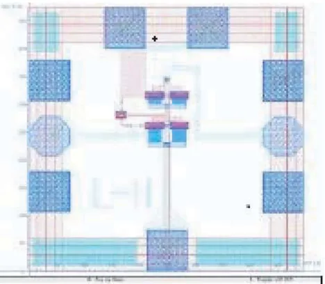
Figure 6 gives the simulated results. To validate the simulated accuracy, Figure 6 also adds the test results. Figure 6(a) and Figure 6(b) depict the simulated results against measured data ofs-parameters and y-parameters. It can be seen that the simulation and measurement results follow the same trends and show good agreements over the whole 4–8 GHz bandwidth. The bandwidth measured for S11 and
Y11 is −6.69 dB (at 5.8 GHz) and −40.58 dB (at 5.8 GHz) from measured data. In Figure 6(c), at the point of 5.8 GHz, the value of simulation is 2.86 nH, and the test value is 2.71 nH. In Figure 6(d), the quality factor of simulation is 8.78, and the test is 8.35. The errors of the simulation results and test results are very small. Furthermore, compared with the calculated value 2.86 nH, the relative error between the simulated and calculated results is only 5.24%. The results indicate that the embedded inductor is fully capable of supporting 5.8 GHz LNA design.
4. CHIP-PACKAGE CO-DESIGN FOR MATCHING NETWORK
4.1. The 3D Co-Design Architecture Based on LGA Package
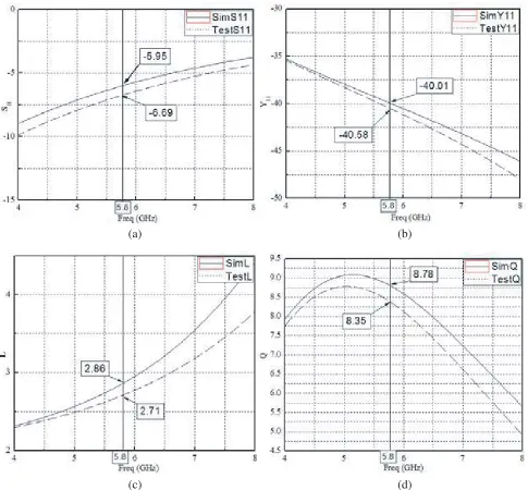
A commercial wire bond LGA package is adopted to perform the chip-package co-design. Figure 7 shows the proposed 3D co-design architecture based on LGA package. The LGA package size is 3.7∗3.9 mm2 with two metal-layers. The unmatched CMOS LNA chip is epoxy-attached to the top layer. The whole model is composed of Source channel, RF input channel and RF output channel. Each inductance should be carefully designed to achieve a good impedance matching. Table 3 provides the prospective values for embedded inductors, which infer from the geometric parameters of on-chip inductors in Table 1.
Figure 7. 3D co-design architecture based on LGA package.
Table 3. Geometric parameters of embedded inductors.
Name Element L(nH) N din (mm) dout (mm)
RF input L2 2 3 0.09 0.27
RF output L3 0.25 2 0.01 0.12
Source L4 0.06 2 0.006 0.012
has the shortest ground vias to connect the top and bottom layers in order to minimize the potential difference between the ground planes. The bond wire diameter is about 25µm. For each wire, the horizontal distance between the first and second bonds is about 700µm, with loop height of 125µm and dies thickness of 300µm. Some papers give the design of a wide-band interface by using bond wires and traces. In those papers, the bond wire is viewed as a high performance inductor applied to a matching network. In this paper, we first devote to developing a common design method of matching network by using embedded inductors while keeping the package parasitic as it is. So the bond wires are designed as short as possible for the smallest parasitic effects, and the main matching networks are designed by embedded inductors.
Table 4. LGA CPW parameters.
Parameter Value
Type Conductor-backed CPW
Dielectric constant 4.2
Dissipation factor 0.002 Tan Substrate thickness 100µm Conductor thickness 10µm
CPW line width 59µm
CPW signal-ground gap 10µm Characteristic impedance 50 ohm
4.2. Extracted Parasitic Parameters
As shown in Figure 7, the RF input channel is composed by embedded inductor, via, trace, bond wire and LGA pad. The RF output channel and Source channel are also composed by them. These transition channels can be accurately modeled by a lumped T circuit to achieve a good impedance matching. Table 5 gives the extracted RLC parameters of RF input, RF output, and Source by ANSYS Q3D.
Table 5. Extracted RLC parameters.
Name R (ohm) L(nH) C (pF)
RF input 1.44 2.35 0.15
RF output 0.74 1.12 0.11
Source 0.59 0.80 0.08
4.3. The Pre-Simulation Results of LNA
The chip-package co-design circuit topology is given in Figure 8. This topology includes one touchstone file of s-parameter and three lumped T circuits of RLC parameters: The touchstone file representing the unmatched CMOS LNA generated from Cadence Virtuoso Analog Design Environment (ADS) and three T circuits representing the parasitic effects from the LGA package modeled by using ANSYS Q3D. Each signal port is terminated to 50 ohm.
The simulation results are shown in Figure 9, where the gain S21, reverse-isolation |S12|, input reflection coefficient S11, output reflection coefficient S22 and Noise figure NF are 3.03 dB, 44.76 dB,
−6.03 dB,−22.46 dB and 3.97 dB, respectively. It is obvious that the input reflection coefficientS11and gainS21do not satisfy the design requirements (S11<−10 dB,S21>10 dB).
Figure 8. Circuit diagram of the LNA with interfaces.
Figure 9. Pre-simulation results of LNA.
5. OPTIMIZATION CO-DESIGN OF LNA
5.1. Frequency Sweep
Impedance matching can be done by a handy calculation through a couple of equations [11]. However, by the assistance of frequency sweep, the impedance matching becomes easier. In Table 6, ten simulation configurations with differentLiand Ls are conducted to find a better compromise between performance and robustness. Considering the importance of inductance for impedance matching, Li
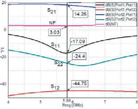
andLsare focused on performing inductance parametric analysis while keeping the resistance (Ri,Rs) and capacitance (Ci,Cs) unchanged. Figure 10 gives the results of input reflection coefficientS11 and gainS21from 5 GHz to 6 GHz. As we can see, the simulated results of Scenarios 3, 4, 5 and 6 measured forS11 and S21 satisfy the design criterions. In this paper, Scenario 5 with Li(3 nH) and Ls (0.1 nH) is preferred as the guide to improve the 3D architecture.
Figure 11 gives the simulation results by using the new values of Li (3 nH) and Ls (0.1 nH). The input reflection coefficient S11 is −17.09 dB, and the gain S21 is 14.26 dB at the frequency of 5.8 GHz, which satisfy the design criterions. Furthermore, the noise figure NF and output reflection coefficient
S22 are lower than the previous results in Figure 9.
Table 6. Simulation configurations.
RF input part Source part
Configuration Ri Ci Li Rs Cs Ls
Scenario 1 1.44 0.15 2.2 0.1 0.02 0.02
Scenario 2 1.44 0.15 2.4 0.1 0.02 0.04
Scenario 3 1.44 0.15 2.6 0.1 0.02 0.06
Scenario 4 1.44 0.15 2.8 0.1 0.02 0.08
Scenario 5 1.44 0.15 3.0 0.1 0.02 0.10
Scenario 6 1.44 0.15 3.2 0.1 0.02 0.12
Scenario 7 1.44 0.15 3.4 0.1 0.02 0.14
Scenario 8 1.44 0.15 3.6 0.1 0.02 0.16
Scenario 9 1.44 0.15 3.8 0.1 0.02 0.18
(a) (b)
Figure 10. S-parameter sweep results: (a) input reflection coefficientS11, (b) gainS21.
Figure 11. Optimized simulation results of LNA.
5.2. Rebuilding 3D Chip-Package Co-Design Architecture
An improved 3D architecture is rebuilt for LNA, as shown in Figure 12. Compared with Figure 7, N
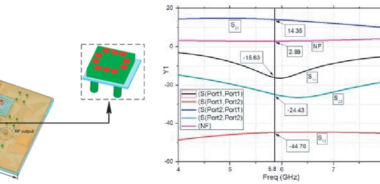
anddout of the embedded inductance in RF input part are increased from 3 to 3.5 and from 0.27 mm to 0.32 mm, respectively. Due to the low inductance in RF output and Source part better for impedance matching, these two embedded inductors are replaced by bond wires and transmission lines, which have inherent parasitic inductors for impedance matching. Table 7 gives the extracted RLC parameters based on the improved 3D chip-package co-design architecture. Compared with Table 5, the full channel inductors of RF input part are increased from 2.35 nH to 3.08 nH, and the RF output and Source inductances are reduced to 0.71 nH and 0.09 nH. By rebuilding the circuit diagram in Figure 8 with the optimized RLC parameters in Table 7, the simulation results are shown in Figure 13. The gain
Figure 12. Optimized architecture based on LGA package.
Figure 13. The results based on optimized structure.
Table 7. Optimized RLC parameters.
Name R (ohm) L(nH) C (pF)
RF input 1.44 3.08 0.15
RF output 0.35 0.71 0.10
Source 0.01 0.09 0.02
Table 8. Performance comparison with on-chip results.
Version On-chip Embedded inductor
input reflection coefficient S11 −19.76 dB −15.63 dB
the gain S21 15.29 dB 14.35 dB
reverse-isolation S12 −31.23 dB −44.70 dB
output reflection coefficient S22 −19.76 dB −24.43 dB
noise figure NF 3.13 dB 2.99 dB
6. CONCLUSION
The main aim of this paper is to analyze and model the LNAs matching networks with embedded inductors for better circuit assembly density and special matching values. After optimizing the 3D chip-package co-design architecture, the gainS21 and input reflection coefficientS11 are improved from 3.03 dB to 14.35 dB and from −6.03 dB to −15.63 dB, respectively. It can be concluded that the novel chip-package co-design technique based on embedded inductors is suitable for 5.8 GHz LNA applications.
ACKNOWLEDGMENT
REFERENCES
1. Lin, Y. C., W. H. Lee, T. S. Horng, and L. T. Hwang, “Full chip-package-board co-design of broadband QFN bonding transition using backside via and defected ground structure,” IEEE Transactions on Components Packaging & Manufacturing Technology, Vol. 4, No. 9, 1470–1479, 2017.
2. Yeh, H. C., C. C. Chiong, S. Aloui, and H. Wang, “Analysis and design of millimeter-wave low-voltage CMOS cascode LNA with magnetic coupled technique,” IEEE Transactions on Microwave Theory &Techniques, Vol. 60, No. 12, 4066–4079, 2012.
3. Li, L., K. Ma, and S. Mou, “Modeling of new spiral inductor based on substrate integrated suspended line technology,”IEEE Transactions on Microwave Theory&Techniques, Vol. 65, No. 8, 2672–2680, 2017.
4. Yue, C. P. and S. S. Wong, “Physical modeling of spiral inductors on silicon,”IEEE Transactions on Electron Devices, Vol. 47, No. 3, 560–568, 2002.
5. Fang, X., R. Wu, and J. K. O. Sin, “Analytical modeling of AC resistance in thick coil integrated spiral inductors,”IEEE Transactions on Electron Devices, Vol. 63, No. 2, 760–766, 2016.
6. Li, S., S. Smaili, and Y. Massoud, “Parasitic-aware design of integrated DC-DC converters with spiral inductors,” IEEE Transactions on Very Large Scale Integration Systems, Vol. 23, No. 12, 3076–3084, 2015.
7. Chuluunbaatar, Z., K. K. Adhikari, C. Wang, and N. Y. Kim, “Micro-fabricated bandpass filter using intertwined spiral inductor and interdigital capacitor,” Electronics Letters, Vol. 50, No. 18, 1296–1297, 2014.
8. Lin, K. C., H. K. Chiou, and P. C. Wu, “2.4-GHz complementary metal oxide semiconductor power amplifier using high-quality factor wafer-level bondwire spiral inductor,”IEEE Transactions on Components Packaging &Manufacturing Technology, Vol. 3, No. 8, 1286–1292, 2013.
9. Xu, X., P. Li, M. Cai, and B. Han, “Design of novel high-Q-factor multipath stacked on-chip spiral inductors,” IEEE Transactions on Electron Devices, Vol. 59, No. 8, 2011–2018, 2012.
10. Mohan, S. S., M. H. M. Del, S. P. Boyd, and T. H. Lee, “Simple accurate expressions for planar spiral inductances,”IEEE J. Solid-State Circuits, Vol. 34, No. 10, 1419–1424, 1999.