177
A Unity Power Factor Multiple Isolated Output
Switching Mode Power Supply Using AC-DC
Converter
Tanupriya sahu
1, Alok Sahu
2,M.K Pradhan
3M.Tech Scholar (Power Electronics), Dept. of Electronics & Communication1,MATS University Gullu-Aarang, Raipur (C.G.)
Asst. Professor, Dept. of electronics & communication2, Gullu-Aarang, Raipur (C.G.)
Head of department, Dept. of electronics & communication3, Gullu-Aarang, Raipur (C.G)
[email protected], [email protected], [email protected]
Abstract-Switched Mode Power Supplies have become increasingly popular for efficient methods of delivering
power to electronic devices. This method of using a current fed push pull converter. While most AC-DC converters utilize a bridge rectifier, the proposed circuit will utilize, this circuit will also inherently provide power factor correction. This power factor correction circuit is capable to perform the AC to DC conversion without the diode bridge rectifier and able to obtain low output voltage. The deal small signal and steady state analysis of the converter operated in discontinuous conduction mode (DCM).AC main switching are, including isolation techniques using opt couplers, to control a bidirectional switch. Simulations results with MATLAB has been shown.
Keywords-PFC; PI controller;Bridgeless rectifier;THD;DCM.
1. INTRODUCTION
SMPS with active power factor correction are necessary for many types of electric equipment to convert line frequency ac to dc output voltage from a major part of load on the utility. Power factor correction is reduce in SMPS the voltage and current distortion and losses. The power quality leading to very low power facto around0.48,the totalharmonicsDistortion (THD) ofinput current is 83.5%. Due to problems associated with low Power factor and harmonics. Thereis converter for step upsuch as buck converter, boost converter, buck-boost converter and Cuk converter .a buck converter is a step-up boost converter it is a SMPS that uses two switches an inductor and capacitor [2].
The bridgeless converter is proposed and this type of DC-DC converter. The non-isolated PFC converter. At the front end of these power supplies is a commonly used. Thebridgeless rectifier reduces the switching losses and conduction loss because of having reduced number of switching. A new bridgeless single-phase AC-DC power factor
E-ISSN: 2321-9637
Available online at www.ijrat.org
178
2. PROPOSED SMPS CIRCUIT
CONFIGURATION AND OPERATION.
A proposed SMPS of configuration based multiple output bridgeless converter using single-phase ac
supply uncontrolled diode bridge rectifier that convert ac voltage to dc voltage. The diode rectifier output is connected to bridgeless buck-boost converter. The working of the proposed SMPS configuration are divided into two subsections and presented as follow
2.1.Buck-Boost converter of operation-
The buck-boost converter a type of DC-DC converter that has output voltage that is either greater than or less than the input voltage magnitude thermal management and low conduction losses, which are not suitable for low power SMPS application the output voltage range is fairly large. A SEPIC and cuk convert working as power factor pre-regulators in c/s such as the converter work as a voltage follower, power factors is unity, the output current ripple was defined at the
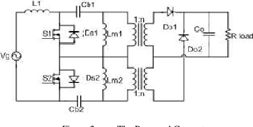
design stage. A simple single-phase bridgeless SEPIC. Bridgeless buck-boost converters. A half-bridge voltage source inverter is used at the output for high frequency isolation and multiple power supplies and it is cast effective compared to push-pull and full-bridge converter the upper and lower buck-boost converter are switched on and off the positive and negative half cycle of the ac volt. The upper buck-boost converter operation of the positive half cycle of the ac input voltage. The lower buck-boost converter operation of the negative half cycle [5]. Figure 1. Two Stage AC-DC PFC
Converter
179
2.2. Half-bridge VSI operation
The half bridge VSI are high frequency isolation the DC output voltage of buck-boost converter. The DC to AC power the upper switch s1 is turnedon, diode D1, D3, D5, D7 start conducting the isolated SEPIC dc-dc converter the foursecondary wounding frequency transformer high frequency
diode D1,D2,D3,D4,D5,D6,D7, D8 and output filter capacitors C01, C02,C03,C04 respectively. A SEPIC stores the energy in an inductor and transformer that energy to the output storage capacitor. When the energy stored in the inductor their maximum values. Thesame operating states respect in each switching cycle.
3. Design of proposed bridgeless converter
based SMPS using AC-DC converter-
The proposed PFC based SMPS are presented the design of switching frequency is very high compared with the frequency line. The steady state analysis of the two stage AC-DC converter based SMPS.A non-isolated AC-DC buck-boost converter is isolated SEPIC.
3.1 Design of non-isolated DC-DC
converter-
The design of a non-isolated back-boost converter is discontinuous conduction mode (DCM) to input converter is designed in SMPS and the calculating different component values is out for the highest rated output [2]. When both high frequency switches (s2 and s3) are off.
Lo1=Vo1 (0.5 – Dn)/ fh×∆iL01 (1)
Where TN=1/fn is the switching time for one PWM cycle, Vdc capacitor value is calculated
C=Idc/2W∆VdC (2) Figure 4
-
Bridgeless converter based multipleoutput SMPS Figure 3. The proposed operated at positive
E-ISSN: 2321-9637
Available online at www.ijrat.org
180 The values of c1 and c2 connected in series. The
proposed SMPS are different component are used
in modeling
.
3.2Design of input filter
The higher order harmonics in the proposed SMPS, it is use of filter to reduce the harmonic distortion of the ac supply
Cmax= Im tanθ/2 ×p × f × Vm (3)
Where Im and Vm are the input ac current and ac voltage.
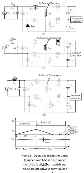
The low harmonic distortion at input ac- Figure 5. Operating modes for under
(a)upper switch Sp is on,(b)upper switch Sp is off,(c)both switch and diode are off, (d)wave forms in one
Ld= 1/4 ×π2 × f2c× Cd (4)
4.
Control of proposed Bridgeless converterbased multiple output SMPS
4.1 Pulse generator PWM
The PWM pulse generator the output of PI controller the fixed high frequencies
ramp is the output of the PI controller saw tooth ramp is less than the switch turn on, it
4.2 Isolated SEPIC for control
The output voltage as input voltage to the SEPIC is DC voltage. Thecontrol of SEPIC is carried out
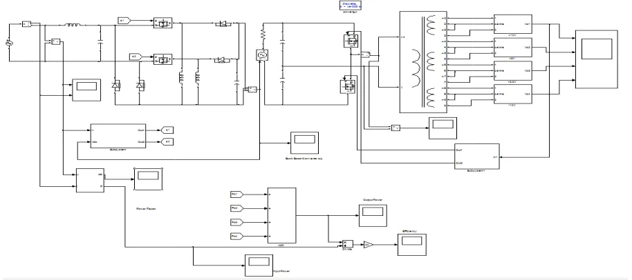
5. MODELING AND SIMULATION
Figure 7.
bridgeless converter based multiple output SMPS of proposed Bridgeless converter
ulse generator PWM
pulse generator the output of PI frequencies saw-tooth ramp is the output of the PI controller saw tooth
on, it is off.
Isolated SEPIC for control
he output voltage as input voltage to the SEPIC hecontrol of SEPIC is carried out
in continuous conduction mode (
The consist of one PI controller and PWM pulse generator [10].
4.3 Non-isolated buck
control
The non-isolated buck-boost converter is designed in DCM. The sensor to sense input current and voltage to regulate the output voltage of the converter. The PWM generator to obtain the ON/OFF control pulse [9].
MODELING AND SIMULATION
Figure 6. Block diagram implementing PI Controller
Figure 7. MATLAB/Simulation of improved bridgeless converter based multiple output SMPS
181 mode (CCM) to reduce. consist of one PI controller and PWM pulse
isolated buck-boost converter for
Available online at
6. ADVANTAGE
1. It will minimize the maximum overshoot
2. Improve Power quality
3. Increased Efficiency
7. APPLICATION
1. Computer&other similarAppliance’s
2.Mobile phone charge.
8. RESULT AND DISCUSSION
This section, simulation results of an
power quality SMPS using bridgeless converter
Figure 8. buck
VSI output voltage.
E-ISSN: 2321-9637
Available online at www.ijrat.org
will minimize the maximum overshoot
ppliance’s.
RESULT AND DISCUSSION
results of an improved SMPS using bridgeless converter
and discussed in details. To study the of the SMPS and if various power specified limits. The simulated SMPS, a step change in
simultaneously on +12V and +5 output. The load on +12V output is varied from 100% to 20%.at 0.15 and simultaneously in +5V, it is varied from 100% to 70% at 0.25s. The
buck-boost converter is maintained small overshoot. Multttipul output remain constant. THD of the input ac mains cu is observed as 5.14% the input current harmonics content is within international stan
unity PF at the utility interface
Figure 8. Input voltage, current, bridgeless buck-boost converter output voltage half bridge VSI output voltage.
Figure 9. Output Efficiency of the implemented circuit
182 in details. To study the performance
The experimentally obtained efficiency of the implemented circuit, as function of the output power,
9.
CONCLUSION & FUTURE SCOPEAn improved power quality SMPS for personal computer application. The input current THD of over 83.5% and PF of less than 16.5 at the utility interface under varying input voltage. It
DC-DC converter has been designed and The first stage DC voltage of the buck converter has been maintained independent of the input voltage is
bridge DC-DC converter is used for obtained multiple DCoutput at the second stage
Figure 10. Power factor output The experimentally obtained efficiency of the
function of the output
Whose minimum value is greater than 80%. The efficiency can be improved by the
soft commutation technique. DC converter has been designed and modeled. first stage DC voltage of the buck-boost Network for more efficient output results.
ACKNOWLEDGEMENT
Authors would like to acknowledge the Department of Science and Technology, Government
for the research grant for the Quality Improvement", under t
from staff of Electronics department of
of Engineering & I.T. I would like to deeply thank ourHead of Department Mr. M K Pradhan and my Guide Mr.Alok sahu and M.Tech coordinator Mr. Figure 11. Output voltage of the converter
Figure 10. Power factor output
183 minimum value is greater than 80%. The efficiency can be improved by the employment of a
the same design can be implemented using Neural Network for more efficient output results.
E-ISSN: 2321-9637
Available online at www.ijrat.org
184 G S Rathore forgiving me the opportunity to apply
and share my knowledge inthis field. I would also like to thanks all the faculties of ourdepartment & every person who have helped me for this paperpresentation.
REFERENCES
[1] Ismail; E.H;April (2009):Bridgeless SEPIC rectifier with unity power factor and reduced conduction losses, IEEE Trans. Industrial Electronics, vol. 56, no.4, pp.1147-1157. [2] Qian Li.;Lee F.C.;Ming Xu, Chuanyun
Wang.;Expositon, (2009)Performance evaluation of bridgeless PFC boost rectifiers,IEEE Energy Conversion Congress,pp. 3755-3760
[3] Abe S.;Yamamato j.;Zeist Tandy Ninomiya T. (2003). Extension of bandwidth of two-stage dc-dc converter with low-voltage/high-current output.Proctor IEEE PESC, Vol.4, pp.1593-1598.
[4] R. KELLER and G. BAKER P (1984) Unity power factor off line switching power supplies, pp.332-339.
[5] K.Matsui; I Yamamoto.; T.Kishi, M.Hasegawa, H.Mori and F.Ueda,I.(02,2002) A comparison of various buck-boost converter and their application to PFC,in 28th conf.IEEE IECON, vol.1, pp.30-36.
[6] N. Mohan.; T. M. Undeland and W. P. Robbins, U (2003) Power Electronics: Converters, Applications and Design, John Wiley and Sons Inc.
[7] P.J.Moore;I.E.Portuguesa.;O.(2003)
TheInfluence of personal computer processing mode on line current harmonics”, IEEE Trans. Power Delivery, vol. 18, no. 4, pp. 1363-1368, Oct 2003. Journal Of Innovative Research & Development Page 608