Generation of Radar Waveform based on DDS
using FPGA and DAC
S Rajesh 1, M R Sanjay Kumar 2, B L Manu Datta3, RRangegowda4 , J Parinitha5
UG Student [ECE], Dept. of ECE, M S Engineering College, Bangalore, Karnataka, India 1,2,3,4 Assistant Professor, Dept. of ECE, M S Engineering College, Bangalore, Karnataka, India 5
ABSTRACT:Communication and digital signal processing applications of today are often developed as fully integrated systems on one single chip and are implemented as application specific integrated circuits using e.g. VLSI technology. As the systems are getting more and more complex, in terms of speed and performance, the chip size and the design time tend to increase rapidly. This will result in search for cheaper and less time consuming alternatives. One alternative is field programmable gate arrays, so called FPGAs. The FPGAs are getting faster, cheaper and the number of gates increases all the time.
The purpose of this paper was to develop a waveform generator to generate arbitrary waveforms based on DDS used for radio/radar applications. DDS technique is widely applicable and simple. Direct Digital Synthesizer (DDS) is a frequency synthesizer and it can generate arbitrary waveforms by using single, fixed frequency reference clock. Some of the DDS Applications are: function generators, modulators. The waveform generator was developed and implemented using a Virtex-6 FPGA from Xilinx and a D/A Converter from Analog Devices. The information of the signal to generate a waveform is programmed using Matlab. In Matlab, we will enter the amplitude, frequency and phase of the waveform to be generated and then load the values of Samples in FPGA RAM. The Data Samples are send to DAC using FMC port. DAC will receive that data from FPGA and then it converts to analog signal. Testing of the whole system, both hardware and software, was done. The system is able to generate sine and chirp waveforms and other arbitrary waveforms.
KEYWORDS:DDS, Radar Waveform, DAC, FPGA, RAM.
I.INTRODUCTION
The aim of this project is to design and implement a DDS architecture on a Field Programmable Gate Array (FPGA). Schematic and VHSIC hardware description language (VHDL) will be used to implement the proposed DDS architecture. The advantage of using an FPGA to implement the DDS is the speed but it also has other advantages. The FPGA behaves according to a “logic function”. The DDS architecture designed can be downloaded onto the FPGA as many times as wanted, there is no limit with different functionalities each time. If there is a mistake in the design, just fix the “logic function”, re-compile, synthesize, build and re-download. Dedicated hardware would most likely require component changes. No PCB, solder or component to change. The designs can run much faster than if a board was to be designed with discrete components, since everything runs within the FPGA, on its silicon die. Then this FPGA will be interfaced with high speed DAC module which is implemented using IC-AD9736[4]. The importance of this IC is that, it provides a better performance between the temperatures -60oc to 85oc. An advantage of AD9736is it operates at high frequency and provides a sampling rate of 1200MSPS. After implementation of the DDS on an FPGA and DAC the performance of the output will be examined in Spectrum Analyzer which show the effect of non-ideal characteristics of building blocks of the DDS on the output spectrum.
II LITERATURE SURVEY
1971. The DDS technique emerged in the early 1980’s and was almost certainly know in theory for quite a few years before that. In those early days, the highest output frequencies attainable was no more than a few megahertz (MHz), limited by the performance of the then available logic Integrated circuits (IC’s) and digital to analogue converters (DACs).
[1]. Chye, Y.H, Ain, M.F.; Zawawi N.M ,“Design of BPSK transmitter using FPGA with DAC”, IEEE 9th Malaysia International Conference 2009.
This paper presents a tutorial exploitation to design and implement BPSK transmitter using field programmable gate array (FPGA) for digital signal processing (DSP), and expansion P240 Analog Module for digital-to-analog (D/A) conversion. The DSP-based BPSK transmitter is developed and compiled to Verilog HDL (Hardware Description Language) netlist. For proper interfacing D/A converter (DAC) with FPGA, a HDL module of configurations of P240 Analog Module and clock synthesizer is integrated with the HDL netlist of BPSK transmitter. Finally, the optimally synthesized netlist of the integrated design is implemented into Xilinx Virtex-4 FPGA MB development board with DAC.
[2]. Ms.Khushboo D. Babhulkar, Mrs.PradnyaJ.Suryawanshi , “Design of Multi-functional High frequency DDS using HDL for Soft IP core” International Conference on Industrial Automation and Computing (ICIAC- 12-13th April 2014) This work presents a highly integrated single chip multi-functional, multi- waveform signal generator which can generate various waveforms, such as sine wave, saw tooth wave, square wave, triangle wave, trapezoidal wave and so on with digital controller inside to adapt embedded and low power applications. The proposed system is composed by Spartan- II, DDS (Direct Digital Synthesis) and other peripherals. Required waveform can be generated by using DDS. [3].B.Suresh, M.V.Srikanth, “Radar Waveform Generator based on DDS”, International Journal of Advanced Research in Computer and Communication Engineering,September 2013
This paper describes radar waveform generator is implemented and it is designed by using directly digital modulation methodbased on DDS. It is able to generate arbitrary signals whose frequency amplitude and phases are controlled by the description words which will be given from external computer. Accurate waveforms are generated. By using Directdigital synthesis technique we can generate waveforms digital.
III. DDS TECNOLOGY
Direct digital synthesis (DDS) [1] is a method of producing an analog waveform usually a sine wave by generating a time-varying signal in digital form and then performing a digital-to-analog conversion. Because operations within a DDS device are primarily digital, it can offer fast switching between output frequencies, fine frequency resolution, and operation over a broad spectrum of frequencies. With advances in design and process technology, today’s DDS devices are very compact and draw little power.
Architecture of Direct Digital Synthesizer (DDS)
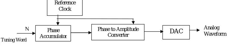
Here is a breakdown of the internal circuitry of a DDS device, its main components are a phase accumulator, a means of phase-to-amplitude conversion (often a sine look-up table), and a DAC. These blocks are represented in Figure 2.1.
Fig 2.1 Components of a Direct Digital Synthesizer.
A DDS produces a sine wave at a given frequency. The frequency depends on two variables, the reference-clock frequency and the binary number programmed into the frequency register (tuning word).
Reference Clock
Phase Accumulator
Phase to Amplitude
Converter
DAC
Tuning Word
N Analog
The binary number in the frequency register provides the main input to the phase accumulator. If a sine look-up table is used, the phase accumulator computes a phase (angle) address for the look-up table, which outputs the digital value of amplitude—corresponding to the sine of that phase angle—to the DAC. The DAC, in turn, converts that number to a corresponding value of analog voltage or current. To generate a fixed-frequency sine wave, a constant value (the phase increment—which is determined by the binary number) is added to the phase accumulator with each clock cycle. If the phase increment is large, the phase accumulator will step quickly through the sine look-up table and thus generate a high frequency sine wave. If the phase increment is small, the phase accumulator will take many more steps, accordingly generating a slower waveform.
Direct Digital Synthesizer Building blocks
A DDS [1] has both analog and digital blocks i.e. it is a mixed signal device. The digital blocks are the Phase Register, Phase Accumulator, and Phase-to-Amplitude Converter. While the analogue block are the Digital-to-Analogue Converter and Reconstruction Filter. The functionalities of each of these blocks of the DDS are discussed in this section.
Phase Accumulator
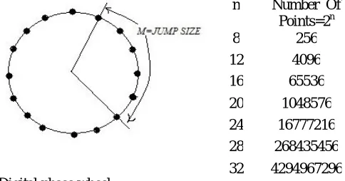
Continuous-time sinusoidal signals have a repetitive angular phase range of 0 to 2π. The digital
implementation is no different. The counter’s carry function allows the phase accumulator to act as a phase wheel in the DDS implementation.To understand this basic function, visualize the sine-wave oscillation as a vector rotating around a phase circle (see Figure 2.2). Each designated point on the phase wheel corresponds to the equivalent point on a cycle of a sine wave. As the vector rotates around the wheel, visualize that the sine of the angle generates a corresponding output sine wave. One revolution of the vector around the phase wheel, at a constant speed, results in one complete cycle of the output sine wave. The phase accumulator (PA) provides the equally spaced angular values accompanying the vector’s linear rotation around the phase wheel. The contents of the phase accumulator correspond to the points on the cycle of the output sine wave. The phase accumulator is actually a modulo-M counter that increments its stored number each time it receives a clock pulse. The magnitude of the increment is determined by the binary-coded input word (M). This word forms the phase step size between reference-clock updates; it effectively sets how many points to skip around the phase wheel. The larger the jump size, the faster the phase accumulator overflows and completes its equivalent of a sine-wave cycle.The number of discrete phase points contained in the wheel is determined by the resolution of the phase accumulator (n), which determines the tuning resolution of the DDS. For an n = 28-bit phase accumulator, an M value of 0000...0001 would result in the phase accumulator overflowing after 228 reference-clock cycles (increments).
Figure 2.2. Digital phase wheel.
If the M value is changed to 0111...1111, the phase accumulator will overflow after only 2 reference-clock cycles (the minimum required by Nyquist). This relationship is found in the basic tuning equation for DDS architecture:
fout= M * fc /2n
where:
fout= output frequency of the DDS
M = binary tuning word
fC = internal reference clock frequency (system clock)
n = length of the phase accumulator, in bits.
Changes to the value of M result in immediate and phase-continuous changes in the output frequency. No loop settling time is incurred as in the case of a phase-locked loop.
As the output frequency is increased, the number of samples per cycle decreases. Since sampling theory dictates that at least two samples per cycle are required to reconstruct the output waveform, the maximum fundamental output frequency of a DDS is fC/2. However, for practical applications, the output frequency is limited to somewhat less than
that, improving the quality of the reconstructed waveform and permitting filtering on the output.
Phase to Amplitude Converter
A phase-to-amplitude lookup table is used to convert the PA’s instantaneous output value into the sine-wave amplitude information that is presented to DAC. In this project, the DDS’s RAM is a sine Look up Table (LUT). The accumulator output represents the phase of the wave as well as an address to a word, which is the corresponding amplitude of the phase in the LUT. This phase amplitude from the RAM LUT drives the DAC to provide an analog output. It is also called a digital Phase-to-Amplitude Converter (PAC), or polar-to-rectangular transformation (projection of the real or imaginary component in time), or (sine) waveform mapping device – a Memory. The lookup memory contains one cycle of the waveform to be generated. The size of the LUT is 2n words. LUT translates truncated phase information, being in digital form, into quantized numerical waveform samples.
Digital to Analog Converter and Filter
The PA calculates a phase address for the look-up table, which outputs the digital value of amplitude corresponding to the sine of that phase angle to the DAC. The DAC, in turn converts that number to a corresponding value of analog voltage or current. The DDS system runs at the same reference clock for synchronization including the DAC. The DAC adds quantization errors at the output to the sine wave. Ideally, Sin(x)/x is used to filter the output of the DAC. It removes the extra frequency components added to the sine wave and hence produces a smooth sine wave.
A DAC is needed to transform the digital sine information into the analog domain. The DAC resolution determines the quality of the output waveform. Inherently, there will be distortion in the sine wave due to the discrete nature of the generation and conversion process. Typically the system is developed such that the error in the output waveform is dominated by the performance of the DAC.
The theoretical noise performance due to quantization error is given by 6.08 + m +1.8dBc
wheremis the effective at-speed linearity of the DAC. DACs are usually specified for their DC linearity, but it is the AC characteristics that determine the noise performance. AC linearity is difficult measure, making it hard to predict actual noise performance of the DAC from data sheet parameters.
Performance of DDS
A DDS has many advantages over its analog counterpart, the phase-locked loop (PLL), including much better frequency agility, improved phase noise, and precise control of the output phase across frequency switching transitions. Disadvantages include spurious due mainly to truncation effects in the NCO, crossing spurious resulting from high order (>1) Nyquist images, and a higher noise floor at large frequency offsets due mainly to the Digital-to-analog converter.
Because a DDS is a sampled system, in addition to the desired waveform at output frequency Fout, Nyquist images are
also generated (the primary image is at Fclk-Fout, where Fclk is the reference clock frequency). In order to reject these
undesired images, a DDS is generally used in conjunction with an analog reconstruction lowpass filter.
III SYSTEM ARCHITECTURE
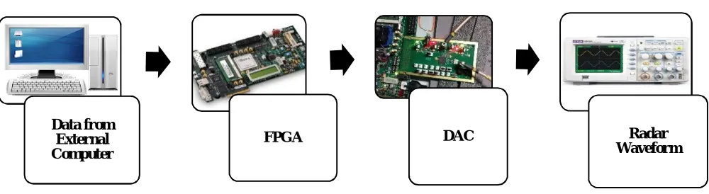
Fig 3.1 Flowchart of Proposed System
A External Computer- The external computer must consist of MATLAB and ISE Design Tool designed for Xilinx-Virtex-6. The digital information of the signal is programed in MATLAB. In ISE, using VHDL description FPGA is configured to store data and clocking management inside FPGA. Details of the ports that are used in interfacing between FPGA and DAC are also entered.
B FPGA - The Virtex-6 FPGA ML605[3] Evaluation Kit provides a development environment for system designs that demand high-performance, serial connectivity and advanced memory interfacing. The ML605 is supported by pre-verified reference designs and industry-standard FPGA Mezzanine Connectors FMC) which allow scaling and customization with daughter cards. Integrated tools help streamline the creation of elegant solutions to complex design requirements.
The important fundamental blocks of FPGA are IBUF, MMCM and OBUF. IBUF converts differential clock pulses to single clock pulse.
MMCM is used for clock management it can provide number of clock pulses of different frequency. OBUF converts single clock pulse to differential clock pulses.
14-bit high speed DAC is connected to FPGA via FMC port.
C DAC- The AD9736[4], is a high performance, high frequency DAC that provide sample rates of up to 1200 MSPS, permitting multicarrier generation up to their Nyquist frequency. The AD9736 is a 14-bit DAC. It includes a serial peripheral interface (SPI) port that provides for programming of many internal parameters and enables readback of status registers. A reduced-specification LVDS interface is utilized to achieve the high sample rate. The output current
can be programmed over a range of 8.66 mA to 31.66 mA. The AD9736 is manufactured on a 0.18 μm CMOS process
and operates from 1.8 V and 3.3 V supplies for a total power consumption of 380 mW in bypass mode. It is supplied in a 160-lead chip scale ball grid array for reduced package parasitics.
D CRO AND SPECTRUM ANALYSER - CRO provides analog information of the waveform that is amplitude and frequency.Spectrum Analyzer provides the information about the non-linear characteristics and harmonics of the waveform.
Data from External Computer
FPGA DAC Radar
V IMPLEMENTATION DESIGN
The implementation of the entire system is carried out as shown in the figure 5.1.
Fig 5.1 Block Diagram of Proposed System
The information of the signal is loaded into the FPGA RAM by using MATLAB and Simulink.
This entire process is carried out in ISE Design Tool designed for Xilinx-Vertex-6.
The data that is taken in by FPGA is buffered.
For the synchronization purpose, management of the clock pulse inside the FPGA is done by MMCM.
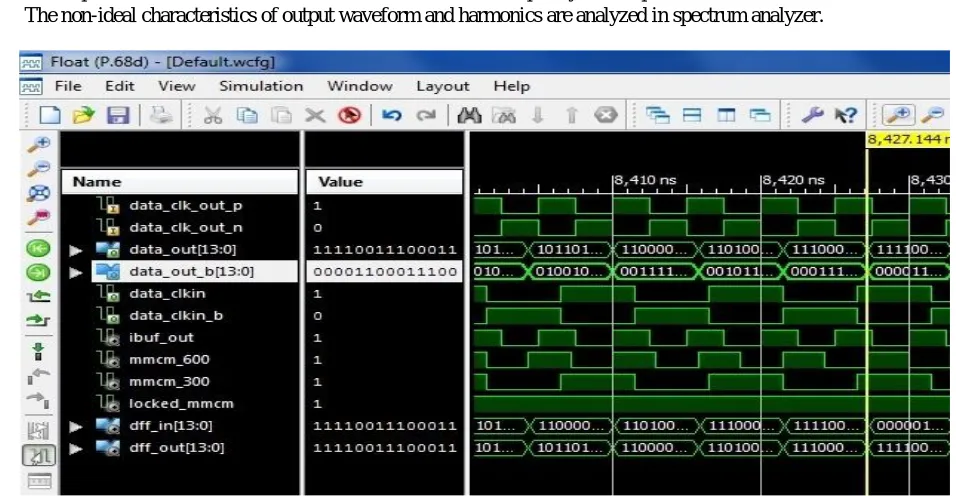
The simulation of the output data is verified in ISE design tool which is given in below figure 5.2.
The interfacing of FPGA and DAC is done through FMC ports.
The discrete sample values which are available in the RAM of FPGA is sent to High Speed DAC module.
Since DAC operates at high frequency and better sampling rate, the data sent by the FPGA is converted to the analog signal with high precision.
The output waveform is taken onto CRO for verification of frequency and amplitude.
The non-ideal characteristics of output waveform and harmonics are analyzed in spectrum analyzer.
Fig 5.2 Simulation of FPGA Code
VI. RESULTS
The figure 6.1 below gives the output waveform across CRO, where in the frequency and amplitude are verified. PC with MATLAB
and Xilinx ISE Design Suite
FPGA
RAM
MMCM
M
14-Bit High Speed Digital to Analog
Converter
Fig 6.1 Sine wave output on CRO.
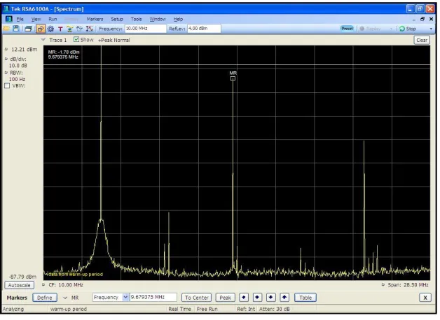
The figure 6.2 below gives the output waveform across spectrum analyzer, the non-linear characteristics and harmonics are verified.
Fig 6.2 Signal Frequency output spectrum.
VI. CONCLUSION
In this paper, the radar waveform generator is designed using FPGA and DAC. This design shows the architecture of radar waveform generator which is designed using AD9736 DAC Module and FPGA.
ACKNOWLEDGEMENT
ECE, M S Engineering College, Bangalore for supporting us in all academic endeavors. Finally, we take respect to all those directly or indirectly helped and encouraged us during the course of the project.
REFERENCES
[1] Ask the Application Engineer—33: All about Direct Digital Synthesis (Analog Dialogue, Vol. 38, August (2004).
[2] Wenfeg Dong, Quan Liu, Shirui Peng and Haihong L “Design and Realization of Arbitrary Radar Waveform Generator based on DDS and SOPC Technology “, ICEMI International Conference, ISBN 978-1-4244-3864-8, pp.16-19 August 2009.
[3] Xilinx Vertex-6 ML605 Evaluation-Kit (www.Xilinx.com). [4] Analog Devices, AD9736 Data Sheet. (www.analogdevices.com).
[5] Zheng Sheng Hua, Xu Dozhuan, JinXueming, Zhang Shishan and Zhang Hongrong “ An Arbitary Waveform Generator for SAR Test-bench Applications”, Microwave Conference Proceedings, APMC, ISBN-0-7803-9433-X, pp 4-7 December 2005
[6] Prakasam.L, Roy.T and Meena.D “Digital Signal Generator and Receiver Design for S-band Radar”, Radar Conference, IEEE, ISBN 1-4244-0284-0, pp. 17-20 April 2007.
[7] Taniza.R, Jadia.K, Raju.G.S.N and Chandra Mohan “High Density FPGA based Waveform Generation of Radars”, Radar Conference, IEEE, ISBN 978-1-4244-5811-0, pp. 10-14 May 2010.
[8] Koenig.F, GoldmanG, Adler E and Conn.M, “Waveform Generation and Signal Processing for a Multifunction Radar System”, IEEE International Conference, ISBN 079803-8234-X, pp.26-29 April 2004.
[9] “Radar Technology “Edited by Guy Kouemou, ISBN 978-953-307-029-2, Publisher: InTech, Chapters published January 01, 2010 under CC BY-NC-SA 3.0 license.
BIOGRAPHY
M R Sanjay Kumar is pursuing his B.E in Electronics and Communications from VisvesvarayaTechnology University, Belgaum.
rom
Rangegowda Ris pursuing his B.E in Electronics and Communications from Visvesvaraya Technology University, Belgaum.
Rajesh Sis pursuing his B.E in Electronics and Communications from M S Engineering College (Affliated to VTU) , Bangalore.
Manu Datta B Lis pursuing his B.E in Electronics and Communications from Visvesvaraya Technology University, Belgaum.