© 2015, IRJET.NET- All Rights Reserved
Page 2134
Design and simulation of low-power ADC using double-tail
comparator
Mr. P. G. Konde
1, Miss. R. N. Mandavgane
2, Mr. A. P. Bagade
31
MTech IVth sem, VLSI, BDCE sevagram, Maharashtra, [email protected]
2
Head of Department, E & Tele.comm engg, BDCE sevagram, Maharashtra, [email protected]
3
Asso. professor, E & Tele.comm engg, BDCE sevagram, Maharashtra, [email protected]
---***---Abstract -
Double-tail comparator is basicallydesigned for SAR-ADC in order to optimize the power with which the circuit operates on high-speed. The circuit is designed under 90 nm CMOS technology means by reducing the technology the parameters get also reduced. The designing of double-tail comparator is based on conventional dynamic comparator and also the circuit is modified by applying the adiabatic logic circuit to the double-tail comparator which is the low-power circuit. The low-power performance results are obtained are improved with the help of adiabatic logic and systematically sizing the transistors of the comparators. Since, the comparator operates on low-power, gives fast speed even in low supply voltages. Similarly, this designing of double-tail comparator is placed between SAR-ADC to optimize the power performance of the circuit and then the ADC circuit reduces the power and operates faster.
Key Words:
DAC, conventional dynamic comparator,
double-tail comparator, adiabatic logic circuit,
SAR-ADC.
1. INTRODUCTION
Analog to digital conversion (ADC) are very important components in electronic equipment. Similarly, Comparator is one of the basic and important building-block in most of the analog-to-digital converter circuits (ADCs).
Designing high speed comparator is more challenging when the supply voltage is smaller. In order to achieve comparator’s high-speed, the larger transistors are required to compensate the reduction of the supply voltages, which also means that more die area and power is needed. Due to fast speed, low power consumption, high input impedance and full-swing output, dynamic conventional comparators are very attractive for many
applications such as high-speed ADC, memory sense
amplifiers and data receivers
.
A comparator consists of a specialized
high-gain differential amplifier. They are commonly used in
devices that measure and digitize analog signals, such as
analog-to-digital converters (ADCs), as well as relaxation
oscillators. A dynamic latched comparator shows higher load drivability than the conventional dynamic latched comparator. The addition of two inverters between the input and output stage of the conventional double-tail dynamic comparator, the regenerative latch stage was
improved. Clocked regenerative comparators are
fundamental circuit blocks, which are mostly based on cross-coupled inverters (latch) to force a fast decision due to positive feedback. This type of comparator is typically used in Flash analog-digital converters (ADCs) because of their high decision speed. After designing the dynamic comparator, double-tail comparator is presented on this basis by adding few minimum-size transistors to the conventional dynamic comparator and also applying the additional circuitry i.e. adiabatic logic circuit which operates on low-power and fast operation even in small supply voltages.
The double-tail topology can operate faster and can be used in lower supply voltages, while consuming nearly the same power as the conventional dynamic comparator. Many high-speed ADC require high-speed, low power comparators with small chip area. Since this newly designed double-tail circuitry is place between SAR-ADC in order to optimize the power performance and the circuit operates on high-speed.
2. LITERATURE SURVEY
© 2015, IRJET.NET- All Rights Reserved
Page 2135
Consumption. In the given technology, Additional circuitry is added to the conventional dynamic comparator to
enhance the comparator speed inlow supply voltages. Due
to the better performance of conventional dynamic comparator in low voltage application, conventional dynamic double-tail comparator is designed on the basis of conventional dynamic comparator which operates on low-power and low supply voltages. The given circuitry has less stacking and therefore can operate at lower supply voltages compared to the conventional dynamic comparator. [1]
Masaya Miyahara et.al developed low-offset latch comparator by using new offset cancellation technique. The developed comparator requires two phase such as reset mode and regeneration mode. The offset voltage of the comparator is caused by the mismatch of the transistor’s threshold voltages. Therefore, due to input common mode variation increasing offset voltage can be suppressed by using the given methodology. The offset voltage cancellation or calibration techniques are vital for realizing a low voltage offset comparator. Conventional double-tail latched comparator had been designed by using conventional latched comparator. Each stage’s contribution to the offset voltage of the conventional comparator obtained from Monte-Carlo simulation. [2]
Jaeha Kim et.al describes a framework based on linear time-varying system theories that can accurately analyse and simulate the random decision error probabilities in clocked comparators. Author presents the analysis and simulation methodologies for characterizing the random decision error probabilities in clock comparators based on an LPTV system model. However, practical comparator circuits do not have such explicit distinction between these filtering, sampling, and decision operations is applicable for understanding the design trade-offs in clocked comparators as well as estimating their random decision error probability using the RF simulation techniques, this mathematical model is useful for analyzing the comparator characteristics and quantifying the decision error probabilities. [3]
Un-Ku Moon et.al implemented the technique which is highly effective for finite op-amp gain compensation in the context of low-voltage and
high-speed pipelined ADCs. This technique enables low-power
and high-speed operation by allowing significantly reduced amplifier gain. Another solution to solve this low op-amp gain problem is the use of correlated double
sampling (CDS) technique. CDS techniques have been used in the design of integrator and amplifier. The most important goals of the time-shifted CDS techniques are to eliminate the one extra clock phase and to realize the pre-sampling and real pre-sampling in different clock phases to avoid added capacitive loading. No offset cancellation scheme is employed because large comparator offsets can be tolerated in pipelined ADCs. The finite op-amp gain is becoming a major hurdle in achieving both high speed and high accuracy. [4]
Sanyi khan et.al developed the technology to analyse the static input offset voltage in a dynamic comparator in the same way as in the traditional operational amplifier. In this paper author presented a novel balanced method to analyze input referred offset voltages in dynamic comparators. The method solves the problem that in a dynamic comparator the operating points of transistors are not well defined in the transient process. In this method, they first solve the bias point at comparison phase when the circuit is perfectly balanced without any mismatch. Second, very little emphasis is placed on mismatch of internal parasitic capacitance [5].
Samaneh Babayan-Mashhadi et.al suggests that UDSM CMOS technology is more reliable for the estimation and optimization of power performance. UDSM CMOS technology has better performance and speed. Double-tail structure takes advantage of input-output isolation and minimum kickback noise, similarly also keeps the advantage of speed enhancement and power reduction. On the basis of the presented analysis, a new dynamic comparator is proposed, where the circuit of a conventional double-tail comparator is modified by using additional circuitry applying to it for low-power and fast operation even in small supply voltages. [6]
© 2015, IRJET.NET- All Rights Reserved
Page 2136
is the low power circuit and handles large power. First, we have to design DAC then counter, comparator, double-tail comparator using adiabatic logic circuit and then finally we have to design SAR-ADC using the developed the binary digital signals, meaningful output appears. Digital-to-analog conversion is a process in which signals having a few (usually two) defined levels or states (digital) are converted into signals having a theoretically infinite number of states (analog). every input bit. It brings into inversion process and gives analog output which varies inversely. It means that if the condition shows that output is directly proportional with the input. The design of DAC using the capacitor array is important for the double-tail comparator in order to provide the proper supply voltage and also to achieve and optimized the performance of the resulting parameters. Capacitor circuits are used to provide accurate voltage gain. A switched capacitor is an electronic circuit element used for discrete time signal processing. It works by moving charges into and out of capacitors when switchesare opened and closed. The use of capacitor array in
© 2015, IRJET.NET- All Rights Reserved
Page 2137
In this designing the interconnection of the various circuit components gives the better result while taking the digital input and then using necessary circuitry the proper and efficient analog output is obtained.
2. COMPARATOR
A comparator is a device that compares two voltages or currents and outputs a digital signal indicating which is larger. A comparator consists of a specialized high- gain differential amplifier. A comparator is designed to produce well limited output voltages that easily interface with digital logic.
2.1 WORKING OF COMPARATOR
PMOS1 PMOS2 PMOS3 PMOS6 PMOS7 PMOS4 PMOS5 Out OutB clk VP fp
NMOS1 NMOS2 NMOS3 VN fn NMOS8 9NMOS NMOS4
NMOS6 NMOS7
NMOS5
Fig3:-Block diagram Conventional dynamic Comparator
This circuitry basically works in two different phases i.e. reset phase and another one is comparison phase.
During the reset phase when CLK = 0. In this condition the transistor Mtail is off and reset transistors
(M7–M8) pull both output nodes Outnand Outpto VDD to
define a start condition and to have a valid logical level during reset.
During the comparison phase, when CLK = VDD. In this condition the transistors M7 and M8 are off, and Mtail is on. Output voltages (Outp, Outn), which had been pre-charged to VDD, start to discharge with different discharging rates depending on the corresponding input voltage (INN/INP).
3. ADC (ANALOG-TO-DIGITAL CONVERTER)
The designing of ADC can be proceeding by placing the conventional dynamic comparator in between ADC. In this condition the analog input is gives to the comparator and the output from the comparator is gives to digital block and it gives necessary digital output value which reduces the power performance in some instant with respect to the comparator and the circuit operates on high-speed.
3.1 WORKING OF ADC
Fig4:- Block diagram of ADC
The ADC circuit is designed by using simple
dynamic conventional comparator which is designed in order to reduce low-power. For this purpose we are firstly designing the 8-bit R2R DAC and it gives analog output which is given to the comparator and it becomes first input of the comparator and the second input to the comparator is an external input supply and it is an analog input voltage. After applying a possible print voltage the process starts and output of the comparator compares both the input voltages at the output terminal and this output is given to the ADC control block which is the main block in this design. The ADC control block compares the overall voltage which takes from the comparator by using load resister which load proper data and finally it compare all the signals comes from DAC and finally gives the proper digital signal or value and consumes and improving a
power performance in greater instant.
SERIAL OUTPUT
clk X3
s1
X1 b6 b7 anainput v X4
vref da X2 DATA MARK
anagnd v b0
b1 b2
cpe b0 b1 b2 b3 b4 b5 b3
b4 start b4 b5
clk b6
clr b7
loadreg
R2RDAC8
Print voltage
Compare datamark
Start Clk clr 0
Reg LH
© 2015, IRJET.NET- All Rights Reserved
Page 2138
4. DOUBLE-TAIL COMPARATOR
Designing of Double-tail comparator can be done on the basis of conventional dynamic comparator by using 90nm CMOS technology.This topology has less stacking and therefore can operate at lower supply voltages as compared to the conventional dynamic comparator. The double tail enables both a large current in the latching stage and a small current in the input stage for low offset. Double tail comparator compares the voltages at both the ends and gives better result and also plays an important role to achieve the power as compared to the simple comparator.
4.1 WORKING OF DOUBLE-TAIL COMPARATOR
S
Fig5:- Block schematic of Double-tail comparator
The double-tail comparator circuit also works in two phases i.e. reset phase and decision making phase. In both this phase’s clock plays a very important role. During Reset phase, CLK = 0, in this condition Mtail1and Mtail2 are off, which avoiding the static power. M3 and M4 pulls both fn and fp nodes to VDD, hence transistor Mc1 and Mc2 are cut off. In reset phase Mc1 and Mc2 are works as control transistors. Similarly, MR1 and MR2 are works as a Intermediate stage transistors. During decision-making phase, CLK = VDD, in this Condition Mtail1, and Mtail2 are on. Transistors M3 and M4 turn off. At the beginning of this phase the control transistors are still off. In decision-making phase Mc1 and Mc2 are works as control transistors. Similarly, MR1 and MR2 are works as a Intermediate stage transistors.
5. ADIABATIC LOGIC CIRCUIT
Adiabatic logic circuits are low power circuits which use “reversible logic” to conserve energy. Adiabatic logic works with the concept of switching activities which reduces the power by giving stored energy back to the supply.
There are two key rules associated with it: 1) Never turn on a transistor when there is a voltage potential between the source and drain.
2) Never turn off a transistor when current is flowing through it.
5.1. BLOCK DIAGRAM OF ADIABATIC LOGIC
CIRCUIT
Fig6:-Block diagram of adiabatic logic circuit
5.2. WORKING OF DTC USING ADIABATIC
LOGIC
Fig7:- Double-tail comparator using adiabatic logic circuit
PMOS NMOS 1
VDD To Double-tail comparator NMOS 2
PMOS NMOS 1
VDD To Double-tail comparator
© 2015, IRJET.NET- All Rights Reserved
Page 2139
In the principle of operation power clock plays an important role in the main design.
When CLK=1, (Charge). When CLK=0, (Discharge).
In this condition the power get reduce in greater instant and also improves the speed of the circuit operates on high-speed. It is very necessary to use adiabatic logic circuit as an extra circuitry for the optimization of power in double-tail comparator circuit. It plays a key role to consume power performance. First by applying adiabatic logic to power supply at the time one transistor is “on” and another one is “off” and vice-versa. This means that at working period it goes into charging condition and at off stage the circuit discharges according to the supply.
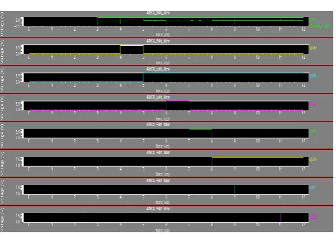
5.3. SIMULATION RESULTS
6. SAR-ADC USING DOUBLE-TAIL COMPARATOR
The Double-tail comparator is basically designed for SAR-ADC which optimized the power performance in greater instant. The designing of comparator consists of adiabatic logic circuit which reduces the power of double-tail comparator design. This designing is placed in between SAR-ADC to handle the large power and by placing the design the power of ADC designed is optimized according to the CMOS technology.
6.1 WORKING OF SAR-ADC
SERIAL OUTPUT
clk X3
s1
X1 b6 b7 anainput v X4
vref Double-tail DATA MARK
anagnd v b0
b1 b2
adj b0 b1 b2 b3 b4 b5 b3
b4 start b4 b5
clk b6
clr b7
loadreg
R2RDAC8
Print voltage
Compare datamark
Start Clk clr
0 Reg LH 1
Fig8:- Block diagram of SAR-ADC
The SAR-ADC circuit is designed by using double-tail comparator which is designed in order to reduce low-power using adiabatic logic. For this purpose we are firstly designing the 8-bit R2R DAC and it gives analog output which is given to the double-tail comparator and it becomes first input of the comparator and the second input to the double-tail comparator is an external input supply and it is an analog input voltage. After applying a possible print voltage the process starts and output of the comparator compares both the input voltages at the output terminal and this output is given to the ADC control block which is the main block in this design. The ADC control block compares the overall voltage which takes from the newly designed double-tail comparator by using load resister which load proper data and finally it compare all the signals comes from DAC and finally gives the proper digital signal or value and consumes and improving a power performance by using
© 2015, IRJET.NET- All Rights Reserved
Page 2140
6.2. SIMULATION RESULTS
5. COMPARISON TABLE AND RESULT
Table -1: Comparison table of parameters
SR NO
DEVICES
PARAMETERS
POWER AREA DELAY
180nm 90nm 180nm 90nm 180nm 90nm
1 DAC 990μW 357μW 129μm^2 3μm^2 1.34ns 1.20ns 2 COMPARATOR 329μW 97μW 256μm^2 2μm^2 940ns 113ps 3 ADC 1950μW 556μW 1100μm^2 170μm^2 4.54ns 6.34ns 4 DOUBLE-TAIL
COMPARATOR
153μW 67μW 392μm^2 2μm^2 294ns 1.24ns
5 DTCUSING ADIABATIC LOGIC
- 59μW - 3μm^2 - 1.24ns
6 ADC USING DTC - 0.06μW - 170μm^2 - 2.69ns
From the above comparison table it is clear that the power performance of the SAR-ADC is optimized in greater instant which is about 0.06μW. Similarly, first we designed the double-tail comparator which gives the power about 67μW. And for better result we are using adiabatic logic circuit for the designing of same comparator which gives the power performance about 59μW. This design is then placed between SAR-ADC block which further optimizes the power as necessary.
6. CONCLUSIONS
We conclude that, the designing of SAR-ADC using UDSM CMOS technology is more efficient for the estimation and optimization of the power performance. This design uses double-tail comparator circuit for the reduction of power and the comparator circuit is simply modified by applying the adiabatic logic circuit to the double-tail comparator which is the low-power circuit and the comparator optimizes the power performance. And by
placing the design in between SAR-ADC the power performance is improved.
REFERENCES
[1] Samaneh Babayan-Mashhadi, and Reza Lotfi, “Analysis And Design of a Low-Voltage Low-Power Double-Tail Comparator” in. proc. IEEE. Int. Midwest Symp. Circuit’s syst. papers, vol.22, Pp.1063-8210, Feb.2014.
[2] B. Goll and H. Zimmermann, “A comparator with reduced delay time in 65-nm CMOS for supply voltages down to 0.65,” IEEE Trans. Circuits Syst. II, Exp. Briefs, vol. 56, no. 11, pp. 810–814, Nov. 2009. [3] A.-J. Annema, B. Nauta, R. van Langevelde, and H. Tuinhout,“Analog Circuiting ultra-deep-submicron CMOS,” IEEE J. Solid-State Circuits, vol.40, no. 1, pp. 132–143, Jan. 2005.
[4] P. M. Figueiredo and J. C. Vital, “Kickback noise Reduction technique for CMOS latched comparators,” IEEE Trans. Circuits Syst. II, Exp.Briefs, vol. 53, no. 7, pp. 541–545, Jul. 2006.
[5] Masaya Miyahara, Akira Matsuzava, “A Low-Offset Latched Comparator Using Zero-Static Power
Dynamic Offset Cancellation Technique,”IEEE A Solid- State Circuits, Vol. 56, No.5, pp. 911-919, May 2009. [6] Chih-Wen Lu, Ping-Yeh Yin, and Ching-Min Hsiao, “A 10-bit Resistor-Floating-Resistor-String DAC (RFR- DAC) for High Color-Depth LCD Driver ICs,” IEEE A Solid-state Circuits, vol. 47, no. 10, October 2012. [7] A. Ali and K. Nagaraj, “Correction of operational amplifier gain error in pipelined A/D converters,” in Proc. IEEE Int. Symp. Circuits and Systems, vol. I, May 2001, pp. 568–571.
[8] S.Babayan-Mashhadi and R. Lotfi, “An offset
Cancellation Technique for comparators using body- Voltage trimming,” Int. J. Analog Integr. Circuits Signal Process. vol. 73, no. 3, pp. 673–682, Dec. 2012.
[9] C.L. Portmann and T. H. Meng, “Supply noise and CMOS Synchronization errors,” IEEE J. Solid-State Circuits, vol. 30, No. 9, pp.1015–1018, Sep, 1995. [10] Jipeng Li, Member IEEE, and Un-Ku Moon, “A 1.8-V 67-mW 10-bit 100-MS/s Pipelined ADC Using Time- Shifted CDS Technique” IEEE J.Solid-state Circuit. Papers, vol.39, no. 8, pp. 0018-9200, Sept.2004. [11] A. Ali and K. Nagaraj, “Correction of operational amplifier gain error in pipelined A/D converters,” in Proc. IEEE Int. Symp. Circuits and Systems, vol. I, May 2001, pp. 568–571.