Building Blocks for a 24 GHz Phased-Array Front-End in CMOS
Technology for Smart Streetlights
Ban Wang*, Gabriele Tasselli, Cyril Botteron, and Pierre-Andr´e Farine
Abstract—According to a recent European Union report, lighting represents a significant share of
electricity costs and the goal of reducing lighting power consumption by 20% demands the coupling of light-emitting diode (LED) lights with smart sensors and communication networks. In this context, this paper proposes the integration of these three elements into a smart streetlight, incorporating a 24 GHz phased-array (Ph-A) front-end (FE). The main building blocks of this Ph-A FE integrated in a low-cost 90 nm complementary metal-oxide-semiconductor (CMOS) technology are fully characterized. The selected FE’s architecture allows the implementation of transceivers as well as Doppler radar sensors functionalities. More specifically, the Ph-A technology is applied to a Doppler radar sensor in order to realize multi-lane road scanning and pedestrian detection. That way, the smart streetlight can become eco-friendly by turning on the LEDs only when necessary as well as to measure traffic parameters such as vehicle speed, type and direction. Intercommunication between the smart streetlights is based on a time-sharing mechanism that uses the same FE reconfigured as transceiver. Thanks to this functionality, the recorded traffic information can be relayed through adjacent streetlights to a control center, and control commands and warnings can be spread through the network. The system requirements are derived assuming a simplified model of the operating scenario with a typical inter-light distance of 50 m and line-of-sight between lights. The radar range is around 60 m, which allows for continuous coverage from one streetlight to the adjacent one. Meanwhile, a communication range of 140 m is derived as a fundamental requirement for reliable communication between streetlight sensors because it allows bypassing of one node in case of failure. For the developed building blocks — a low-noise amplifier, a variable-gain amplifier, a voltage-controlled oscillator and a vector modulation phase shifter — the design methodology is presented together with measurement results. The system power, consumption, noise figure and gain are estimated by means of a system analysis based on the measured data from the implemented blocks and the state of the art performances for the missing parts. It is shown that the requirements can be fulfilled with a total power consumption of around 375 mW in Doppler radar sensor mode and around 190 mW in transceiver mode. To the authors’ knowledge, this kind of integration is new and overcomes some limitations of the currently used solutions based on infrared sensors and low-throughput communications.
1. INTRODUCTION
In line with European Union legislation to phase out incandescent light bulbs in streetlights by the end of 2016 [1], some important researches have been done in the past few years to develop light-emitting diode (LED) light sources with additional smart functionalities. Most of the research in this area focuses on wireless networking between lamps by using a standard protocol such as ZigBee [2]. Currently, there are few reliable movement sensors on the market. Indeed actual passive infrared sensors are not able to cover the whole illumination area of a streetlight and are very sensitive to environmental influences
Received 18 June 2014, Accepted 17 October 2014, Scheduled 27 October 2014
* Corresponding author: Ban Wang ([email protected]).
like rain or snow. Different field tests have shown that there are some reliability problems with infrared sensors in the range of about 10 m [3]. Only a few developments have targeted the integration of wireless sensors to add sensing features to the LED lamps [4]. Moreover, the high density of streetlights would be an ideal platform for an intelligent sensor network to monitor the road network and the environment. To upgrade the huge number of streetlights, an extremely low-cost solution is required. Complementary metal-oxide-semiconductor (CMOS) technology enables a low-cost implementation of complex systems on the same chip (system on chip, SoC). Furthermore, integration of the sensor and the LED streetlight can profit from the ceramic substrate used to dissipate the heat produced by LEDs. The high relative permittivity and the low losses of the ceramic substrate allow the implementation of miniaturized and high-performance printed circuits at mm-wave [5]. For example, a very compact radar antenna array is reported in [6], where a 36 GHz four-patch antenna array is smaller than 1 cm2.
The industrial, scientific, and medical (ISM) band at 24 GHz is accepted worldwide for short-range communication and for radio determination [7, 8]. Since a wide band, i.e., 250 MHz, is available, a simple binary phase-shift keying (BPSK) modulation carrying some Mbps enables the allocation of more than 10 channels. Considering the duty cycle between the radar and transceiver modes (e.g., 10%), the net data rate could easily exceed the ZigBee’s throughput (100 kbps) already proposed for streetlight networking.
The development of a 24 GHz integrated circuit (IC) radar front-end (FE) started in 2003 with silicon germanium (SiGe) technology [9] by M/A-COM Technology Solutions. It continues today, especially for automotive radar, as well as in many silicon foundries, e.g., STMicroelectronics, Philips and Motorola [10–12]. In the last five years, some implementations of the main building blocks and complete FEs have also been developed in CMOS technology by university groups [13]. Phased-array (Ph-A) technology was developed during World War II, and it continues to be used mainly in military radars. Recently, increasing attention has been focused on the research of the Ph-A technology for civil applications, such as automotive radars in CMOS technology [14]. However, chipsets are still hardly available on the open market for general purpose applications. To the best of our knowledge, there is only the BGT24MTR11 by Infineon Technologies [15], which works at 24 GHz and is based on SiGe monolithic microwave integrated circuit. Moreover, this product does not use the Ph-A technology.
In this paper, a novel approach of the 24 GHz CMOS IC FE, which is based on our previous work [16–18], is proposed. This FE uses the Ph-A technology for the Doppler radar sensor and integrates an extra transceiver communication channel that can be used in a time-sharing mechanism.
2. SYSTEM DESCRIPTION AND ANALYSIS
2.1. System Description
One advantage of working at 24 GHz is the quite high Doppler shift, about 44 Hz per km/h, which allows the detection of a slow moving target with only few hundreds of milliseconds of measurement time. It entails that the FE does not need to work continuously as a radar.
communication. By using a direct-conversion receiver and a direct-modulation transmitter, it is thus conceivable that a single FE may fulfill the radar and communication functionalities in time-sharing, by implementing a communication duty cycle of around 10%, i.e., using a data rate 10 times faster than the required throughput.
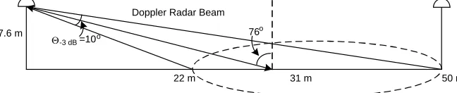
Figure 1 shows the streetlight application scenario and the functionalities implemented by the Ph-A FE. Typical parameters of the streetlight deployment are 7.6 meters in height and 50 meters in inter-distance [20]. By pointing the main antenna beam towards the sidewalk, the Doppler radar sensor can detect the presence of pedestrians and turn on the streetlights only when people are detected. Similarly, by pointing the antenna towards one of the road lanes, it is possible to detect the presence of cars and measure their speeds and lengths, as well as recognize their moving directions. When the FE works as transceiver, communication between streetlights is enabled, thus building up the hardware for a wireless sensor network (WSN). The streetlight files can be organized in a hierarchical network that enables each node to communicate with a control center. This is a powerful feature that allows the collection of a lot of information, such as the presence of faults, and real-time road traffic conditions. Moreover, profiting from the 250 MHz bandwidth, a frequency division technique can be used, for example, adjacent FEs could use different carrier frequencies, i.e., f1 to fn, in order to improve the robustness against radar and transceiver interferences. In the event of fault of one or more transceiver, the control center can locate the fault and change the frequency plan to bypass the out-of-order ones.
From the description given above, it is clear that the antenna system is a key element of the Ph-A FE. Indeed, in radar mode, a beam-steering antenna with a relatively narrow beam is needed. Ph-A further advantage of working at 24 GHz is the antenna dimension, because the in-air wavelength is only 12.5 mm. For inter-communication, a fixed antenna with limited directivity is preferable in order to allow links with multiple FEs. To fulfill the different requirements, two types of antennas are supposed to be used.
The radar antenna array is assumed to be a patch array antenna type; indeed it could be directly printed on the ceramic substrate usually used as LEDs carrier for heat dissipation. In this case the beam is pointed towards the ground. However, as shown in Figure 2, it should be tilted by about 76◦ in order to point towards the vehicle incoming direction as well as at the halfway point between two streetlights. This tilt is achievable by embedding fixed delay lines in the patches feeding transmission lines.
For inter-communication, a fixed antenna with limited directivity is preferable in order to allow links with multiple FEs. Therefore the inter-communication link exploits two dedicated antennas for
Wireless Sensor Network
50 meters 7.6
meters detectionPerson detectionCar Multi-lanedetection Control center
0
f f1 f2 f0
Figure 1. Sketch of the proposed scenario and the functionalities implemented by the Ph-A FE.
7.6 m
50 m Doppler Radar Beam
=10
Θ-3 dB
22 m 31 m
76
o
o
transmitter (TX) and receiver (RX), less directive than the radar case, pointing towards the adjacent streetlight. The wireless link between the streetlights can be nearly treated as a line-of-sight point-to-point communication.
2.2. Additional Antenna Considerations
A complete analysis with electromagnetic models is beyond the scope of this paper. However, there are several examples of antenna design at 24 GHz for radar applications. In this paper, we refer to [19], where two antenna arrays of 10×4 patches each one were used as TX and RX antennas. Such an antenna array can be viewed as the combination of four sub-arrays where each one consists of 10 elements in-line. Thus, the four linear sub-arrays can be paired with the four channels of a Ph-A FE, in which case the beam steering can occur along the same direction of the shorter side of the antenna. The corresponding 3 dB beamwidth can be calculated by the simple model equation presented in [21]: for a linear array, the half-power beamwidth is approximated by Θ = 101N.8◦, whereN is the number of elements. Thus, in our case, a 10×4 element linear array will have a 3 dB beamwidth along the larger and smaller array side, of about 10◦ and 25◦, respectively. The same antenna array was characterized in [22], where the reported 3 dB beamwidth was 10◦ for the larger array side and 28◦ for the smaller side. These figures are closed to the ones obtained with the simple model calculation aforementioned. Moreover, in [22], the antenna gain was 17.6 dB and the mutual coupling between RX and TX was not a limiting factor due to the intrinsic rejection of the homodyne receiver used in the Doppler radar scheme. Therefore, we consider that a 10×4 antenna array is sufficient to fulfill the requirements of the selected application. Antenna sidelobes can also affect the radar sensor performance, e.g., affecting the scanning selectivity and the capability of the radar to classify vehicles per lane, or affecting the capability of the system to detect moving objects when two different objects with various speeds are seen by the radar. However, the effects of the antenna sidelobes can be minimized by controlling the radiated power level so that the sensitivity of the system is adjusted to detect only the strongest Doppler echo and/or by filtering the Doppler estimation with a second step of calculation, for example by performing the calculation of the histogram of the Doppler frequencies detected. If two or more peaks are shown, the processing can understand the presence of two or more vehicles. It requires more processing but it is still possible with standard embedded microprocessors.
2.3. System Analysis
Based on the assumptions made above, the estimation of the system specifications is discussed next. Since there are two system operating modes, the analysis is carried out for both modes.
2.3.1. Doppler Radar Case
Working in radar mode, Eq. (1) shows the well-known radar free-space path loss (PL) equation [23]:
P Lradar(dB) =−10 log c
2σ
f02(4π)3R4
, (1)
wherecis the speed of the light, f0 the operating frequency, i.e., 24 GHz,R the detection range, and σ the radar cross section of the target, which is assumed to be 0.1 m2 from [24].
Recalling that the receiver sensitivity is given by the sum of the minimum signal-to-noise ratio (SNR), the noise figure (NF) and the thermal noise power, the radar range can be written as a function of PL (Eq. (1)), therefore the Friis transmission equation can be written as [23]:
P Lradar(dB) =PT X−NFradar +GT X,sub+GRX,sub−Pnoise
−SNRmin+CP GT X +CP GRX −LM −2×Lη, (2)
where:
PT X is the transmitted power for a single channel, which is assumed to be about 1 dBm in order to keep a low consumption and to deal with the low-voltage power supply of 90 nm technology.
NFradar is the noise figure of the single channel receiver, which is assumed to be about 6 dB based
GT X,sub and GRX,sub are the gain of a 10-patch λ/2-apart linear array, which is estimated to be around 16.7 dB by simulation with basic models.
Pnoise is the thermal noise power for each channel, which is estimated by the equation: Pnoise(dB) =
−174 + 10 logBWn. In this equation, the equivalent noise bandwidth of the Doppler radar system,BWn can be set according to the Doppler frequency shift fD. The latter can be written as fD =f02cv cosα, where f0 is the carrier frequency, i.e., 24 GHz; α is the angle between the antenna pointing and the direction of the moving target; and v is the target velocity, which is assumed to be lower than 250 km/h. So the maximum Doppler shift, fD,max is around 11 kHz since the Doppler shift constant is 44 Hz per km/h. Consequently, the BWn can be assumed for a first-order filter to be equal to: fD,max×π2 ≈18 kHz. Therefore, Pnoise is calculated as −131.5 dBm.
SNRmin is the minimum SNR of the Doppler radar, which is assumed to be 12 dB because of the highly sensitive detection methods usually employed [25].
CP GT X and CP GRX represents the coherent process gain, which reflects the power and SNR enhancement of the Ph-A technology. It can be explained easily by assuming an N channel Ph-A transmitter with each single channel of P watts of emitting power. Along the pointed direction, the waves add coherently producing an amplitude N times bigger than the single channel, so the power is
N2P watts. Therefore, the power gain is 20 log(N) in dB. In reception, the Ph-A enhances the SNR of N times because of the coherent addition of the useful signals and the incoherent addition of the noise (10 log(N) in dB) [26]. For a four-channel Ph-A, theCP Gis 6 dB and 12 dB for the receiver and transmitter respectively.
LM is the link margin, which is assumed to be 10 dB. This margin could also include any antenna mismatch. However, it is assumed that the antennas are well matched, so that the mismatch is negligible.
Lη represents the array efficiency and takes into account the losses due to the combination of the Ph-A channels [27]. It can be roughly estimated of 2 dB, by comparing the antenna gain of a 10×4 array (∼21.4 dB) with the theoretical combination of four isolated 10-element linear arrays. The losses are 16.7 dB + 6 dB−21.4 dB = 1.3 dB.
Upon substituting the assumed values mentioned above in Eq. (2), the PL of the radar mode can be calculated as 152 dB. Furthermore, the sensitivity of the receiver can also be calculated as−113 dBm.
The final step is to estimate the radar detection range by inverting Eq. (1). The radar detection range corresponds to around 60 m, which gives a sufficient margin over the required 50 m of the studied scenario.
2.3.2. Transceiver Case
The inter-streetlight communication can use smaller and less directive antennas, pointing towards the nearby streetlights. Moreover, a single-channel transceiver is used because the beam steering feature is not necessary so the coherent process gain is not exploited. With a methodology similar to the previous case, the PL from the Friis formula can be written as:
P Lcom.(dB) =PT X,com.−NFcom.+GT X,com.+GRX,com.−Pnoise,com.−SNRmin,com.−LM. (3) The meaning of each term is discussed as follow:
PT X,com. and NFcom. are kept the same as the radar case because of the hardware reuse, and are 1 dBm and 6 dB respectively.
GT X,com. and GRX,com. are the antenna gains, which are estimated to be around 14.9 dB by simulating a 2×4 patch-array antenna with basic models.
Targeting a net data rate of 1 Mbps and assuming a duty cycle of 10% for the data transmission, the necessary peak data rate must be 10 Mbps. Exploiting a simple BPSK modulation, considering the bit error rate of 10−6 and no coherent demodulation, theSNRmin,com.is assumed to be 12 dB [28], and the channel bandwidth is around 25 MHz (so there are up to 10 channels in the ISM band).
Under these assumptions, the noise power floor,Pnoise,com. is equal to −100 dBm, and thus entails a sensitivity of−82 dBm.
By applying Eq. (3), a maximum PL of 103 dB is estimated and applying the one way free-space PL equation [23], we have
P Lcom.(dB) =−10 log c 2
A maximum communication range of 140 m is obtained. Since the range is more than twice than the distance between two adjacent streetlights, it will be possible, in case of node fault, to leap over one or two streetlights and communicate with the next in the line.
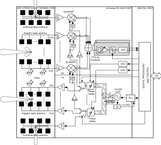
2.4. Proposed ASIC Architecture
Based on the system analysis, a four-channel Ph-A architecture as shown in Figure 3 is proposed. This FE consists of two parts: the antenna arrays and the application-specific integrated circuit (ASIC) front-end; meanwhile the digital back-end is out of the scope of this paper. The antenna part has two types of antennas: the 10×4 patch-array antenna used for the Doppler radar sensor and the 2×4 patch-array antenna for inter-communication. The radar type is the continuous-wave (CW) Doppler radar, which does not rely on any modulations to separate the radiated signal to the reflected one. This type of radar is robust to the coupling between TX and RX paths. The homodyne scheme can split the generated CW signal to feed the TX antenna and the RX mixer. The parasitic coupling between TX and RX antenna and circuits will be in any case smaller than the direct signal from the local oscillator (LO) and the RX mixer. The problem does not exist in transceiver mode due to the half-duplex working mode.
The ASIC FE consists of a direct-conversion receiver and a direct-modulation transmitter. A dedicated RF channel is used for the transceiver mode, while the baseband is reused. In this case, even if consuming a bit more chip area, no antenna switches are needed and the symmetry of the main four-channels can be preserved. The core of the Ph-A scheme is a 24 GHz phased-locked-loop (PLL) frequency synthesizer combined with a vector modulation phase shifter (VMPS). The phase shifters provide beam-forming functionality in radar mode as well as direct BPSK modulation in transceiver mode. The four VMPS outputs are split in order to contemporaneously feed the RX and TX paths as required by the continuous-wave Doppler radar scheme. The additional RX and TX paths for the transceiver are switched off during radar mode. For the radar RX paths, the VMPSs provide the
phase-DIGITAL PART mm-wave FE ASIC PART
90°
Q
LNA
LN
A
PA
ϕ
PA
I
VGA VGA
ADC
DAC DAC RX
TX
Phase Shifter IQ-MIXER
OTA as Combiner
24 GHz VCO
Phase Shifter 90°
IQ-MIXER CH1
PLL :16 CH4
DIGITAL PROCESSING
AND CONTROL
I/O
1.5 GHz 0
180 90 90 CH1
CH4
BUF BUF
LNA
90°
BUF Communication antenna
Doppler radar antenna
LEDs LED STREETLIGHT CERAMIC PCB
Doppler radar antenna
Communication antenna
PA
° °
ϕ
° °
shifted LO signals to the mixers. Complex down-conversion is adopted so that the down-converted signals have the in-phase (I) and quadrature (Q) components. Thus, each channel of the Ph-A has a couple of mixers.
At the mixers outputs, the aforementioned coherent addition of the wanted signals and the rejection of the interferences take place. The resulting I and Q signals are processed in parallel by two identical baseband paths, consisting of: a low-pass filter (LPF), a variable-gain amplifier (VGA) and a multi-bit analog-to-digital converter (ADC). The baseband is shared in time division between transceiver and radar modes, therefore the LPF has to be reconfigurable in order to adapt the cut-off frequency to the wide bandwidth of the transceiver and the narrow bandwidth of the radar.
In the radar TX paths, the four phase-shifted signals are amplified to reach a power level of about 1 dBm on each channel. Thanks to the Ph-A architecture and the constant amplitude modulation, such a compression point is achievable also with a low-voltage power supply (1.2 V). By controlling the state of several switches in the RF paths’ DC biases, the digital unit can manage the mode switchover so that a power-saving management is implemented by turning off the unused blocks.
3. CIRCUITS DESIGN AND MEASUREMENT RESULTS
The key building blocks, namely the LNA, the VGA, the VMPS and the voltage-controlled oscillator (VCO), were designed in 90 nm technology by United Microelectronics Corporation (UMC). The technology offers nine metal layers with a top layer thickness of 3µm for high-Qinductors and scalable
M0 M1 L L C C RFin RFout C C R M2 R G G R G G V V 24 0.09 24 0.09 2 0.09 500 fF
60 fF 1 nH
300 pH
200 Ω
200 Ω
6.7 kΩ
120 fF 60 fF (a) (b) -2 10 8 6 4 2 0 3.8 5 4.8 4.6 4.4 4.2 4 2.8 3.6 3.4 3.2 3
20 22 24 26 28 30
Sim. typ Meas
Noise Figure (dB)
S (dB)21 Frequency (GHz) Sim. NF -16 -2 -4 -8 -10 -12 -14 S (dB)11 -18 -6 Sim. typ Meas
20 22 24 26 28 30
Frequency (GHz) (c) (d) dd g p b b op os 2 s
Figure 4. Single-stage LNA schematic, die photo, simulated and measured S-parameters.
models for passive RF components. RF metal-oxide-semiconductor field-effect transistors (MOSFET) haveVmax of 1.2 and 1.8 V. The designed blocks were implemented in a test tape-out with the purpose of refining the methodology used for the parasitics estimation.
The measured results shown below are all taken on-chip by using RF probes calibrated at the on-chip pads’ plane.
3.1. Low-Noise Amplifier
The LNA design is based on a cascode amplifier as shown in Figure 4(a). Since little power gain is available at 24 GHz due to the MOSFET gain roll-off, the cascode configuration is used to increase the gain. For the same reason, and to get a better estimation of the parasitic ground inductance, the source inductor, commonly used for the simultaneous matching of the noise and gain, is omitted. All MOS transistors have a minimum length, i.e., 90 nm, and each cascode MOS has a total width of 24µm obtained by connecting in parallel 24 fingers each 1µm wide. The resulting MOS current density is almost 150µA/µm, which is not far from the 250µA/µm for the transition frequency (fT) peak. The current-density reduction is due to the limited voltage headroom for the upper MOS, M1, which does not have the necessary overdrive (around 0.5 V) for the fT peak. In Figure 4(c) and Figure 4(d), the measured gain and return loss are compared with the simulation results. The latter is based on the extracted layout view obtained by using the standard extraction tool available in Cadence. The peak gain of 6.5 dB at 24.1 GHz is 2 dB lower than the simulated results, and the peak return loss is 4 dB better. The peak frequency also occurs exactly in the middle of the ISM band. Based on this comparison, the extraction method shows a quite good performance.
The noise figure cannot be measured with the available instrumentation because of the low LNA gain, and therefore the simulated NF of 3.2 dB is reported while an input referred 1 dB compression point (IP1 dB) of −12 dBm has been measured. Finally, the LNA power consumption is 4.3 mW at 1.2 V.
A gain of only 6.5 dB is certainly insufficient to set the receiver NF at the desired level of 6 dB, therefore, a three-stage LNA has been designed. It is based on a cascade of three cascode amplifiers as shown in Figure 5(a). The first stage is almost identical to the previous single-stage LNA; the second stage uses the MOSs with the same parameters but its matching networks are embedded in the previous and following stages. The third stage uses bigger MOSs, i.e., 60µm wide, since it needs to boost the output compression point at about 1 dBm. Measurement results, reported in Figure 5(c) and Figure 5(d), show a peak gain of 18.6 dB at 23.9 GHz and a return loss of−16 dB. A considerable frequency down-shift is visible as well as a gain loss of about 5 dB. In this case, even if process variations are taken into account, the parasitic extraction method does not perform well.
The measured NF of 5.5 dB is also well above the simulated 3.8 dB. On the other hand, the output 1 dB compression point is about 2 dBm as was expected. The power consumption is 18 mW at 1.2 V.
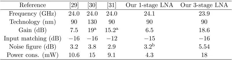
In Table 1, the LNAs’ performances are compared with the state of the art. The single-stage LNA consumes less than one half the power of an amplifier with similar gain and noise figure. The three-stage LNA shows almost the same gain as the other multi-stage amplifiers but generates more noise while consuming 20% more power. If its peak gain were like the simulated one, the comparison would have been favorable.
Table 1. 24 GHz LNA specification comparison.
Reference [29] [30] [31] Our 1-stage LNA Our 3-stage LNA
Frequency (GHz) 24.0 24.0 24.0 24.1 23.9
Technology (nm) 90 130 90 90 90
Gain (dB) 7.5 19a 15.2a 6.5 18.6
Input matching (dB) −16 −16 −12 −15 −16
Noise figure (dB) 3.2 3.8 2.9 3.2b 5.54
Power cons. (mW) 10.6 15 9.1 4.3 18
3.2. Analysis of Parasitic Effects of the LNAs’ Layouts
To investigate the parasitic effects of the LNAs’ layouts, the measurement results and the extracted post-layout simulation results are compared. As shown in Figure 4 and Figure 5 and summarized in Table 2, these results do not match very well, especially for the three-stage LNA. It is likely that the
M0 M1 Lc 1 Lg Cs1 RFin Rb1 Cp Cs M7 G G R Rb2 RF out G G M3 M2 Lc2 Cs2 R M5 M4 Lc 3 Cs out R Cpout Rb 3 M6 Vdd Vb1 Vb2 24 0.09 24 0.09 60 0.09 500 fF 60 fF 1 nH
6.7 kΩ 200 Ω300 pH
120 fF 120 fF 60 fF 2 0.09 2 0.09 (a) (b) -5 25 20 15 10 5 0 7 10 9.5 9 8.5 8 7.5 6.5 6 5.5 5
20 22 24 26 28 30
Noise Figure (dB)
S (dB)21 Frequency (GHz) -20 0 -5 S (dB)11 -25
20 22 24 26 28 30
Frequency (GHz) (c) (d) -10 -15 Sim. typ Meas Sim. NF Sim. typ Meas
Figure 5. Three-stage LNA schematic, die photo, simulated and measuredS-parameters. (a) Schematic
of 3-stage LNA. (b) Die photo of 3-stage LNA. (c) Simulated and measured LNA gain. (d) Simulated and measured LNA return loss.
Table 2. LNA parasitic analysis with the comparison of Gain @ 24 GHz, NF and input matching.
Gain (dB) NF (dB) Input matching (dB) 1-stage LNA
Measurement 6.5 N/A −18.3
Extracted post-layout 8.2 2.98 −12.4
Manual parasitic 6.5 3.52 −9.9
3-stage LNA
Measurement 18.62 5.54 −19.2
Extracted post-layout 23.9 3.4 −12
M0 M1 L2 Lg Cos Cop RFin RFout Cp Cs Rb M2 R R Vdd Vb Pad lumped equiv. circuit Lin Ls Rs Lvdd Cdrain Pad lumped equiv. circuit Cf Trans. Line in layout
60 m
Trans. Line 24 0.09 24 0.09 2 0.09 Rin Cin Cf Cf M0 M1 Lc1 Lg Cs1 RFin Rb1 Cp Cs M7 R Rb2 RFout M3 M2 Lc2 Cs2 R M5 M4 Lc3 Cs out R Cpout Rb3 M6 Vdd Vb1 Vb2 Pad lumped equiv. circuit Pad lumped equiv. circuit
Lvdd Lvdd Lvdd
Trans. Line in layout
Ls Rs
Ls
Rs RsLs
Lin Cf
Cdrain Cdrain Cdrain1
Cgate Rin
24
0.09 0.0924 0.0960
2 0.09
2 0.09
(a) (b)
Figure 6. Parasitic schematic of the single-stage and three-stage LNAs. (a) 1-stage LNA parasitic
schematic. (b) 3-stage LNA parasitic schematic.
inaccuracy comes from the parasitic extraction method implemented in the CAD tool. In order to get an in-depth understanding of the extraction methodology, a specific analysis was carried out. It was done by working at the schematic level and adding the key parasitic elements shown in red in Figure 6, namely: on-chip pads, microstrip lines for long connections, input series resistanceRs, source inductance Ls on cascode grounding, coupling capacitance Cf between input and output of the cascode amplifier, and tuning capacitances/inductances in parallel/series with the resonators.
For test purposes, some structures, such as transmission lines, RF pads and inductors, were included in the chip to allow their modeling. Specifically, Lin and Lvdd account for 10% tolerance ofLg and L2 values; Ls is estimated to be around 50 pH and Cf is estimated to be about 4 fF. The transmission lines are modeled by microstrips with their physical length and the substrate model provided in the technology datasheet. Finally, the equivalent resistance in series with the gate, Rs, is estimated by adding the DC resistances of the vias and the metal paths.
Figure 7 shows a comparison between the schematic with parasitic and the measurements of the two developed LNAs. For the three-stage LNA, the same parasitics determined for the single-stage LNA are applied and only a slight tuning of the resonate loads is necessary for a good fitting. The parasitics modeling seems quite robust thanks to the physical model used. The reason why the extraction tool in Cadence does not work very well at 24 GHz is not clear. The main mistake seems to be related to the estimation of the resistance in series with the gate. Indeed the 2 dB error of the noise figure is quite high. Also the coupling between inductors seems not to be considered even if the coupling option is selected. Finally, the schematic with parasitics shows a difference of less than 2 dB for the gain and 0.3 dB for the NF.
3.3. Variable-Gain Amplifier
-20 0
-5
S
(dB)11
-25
20 21 22 23 24 25
Frequency (GHz)
(d)
-10
-15
S model
26 21 22 23 24 25
Frequency (GHz)
26
11
S meas11
S model21
S meas21
S model11
S meas11 S model21
S meas21
-10 10
5
0
-5
S
(dB)21
-30
-20 0
-5
-25 -10
-15
-30
-35
-40
S
(dB)11 5
25
20
0 -15
10
-5
-10
S
(dB)21
23
21 22 24 25
Frequency (GHz)
26 21 22 23 24 25
Frequency (GHz)
26
(c)
(b) (a)
Figure 7. LNA parasitic models and their measurement results. (a) Measured and simulated S11 of
1-stage LNA: parasitic modelled. (b) Measured and simulated S21 of 1-stage LNA: parasitic modelled. (c) Measured and simulated S11 of 3-stage LNA: parasitic modelled. (d) Measured and simulated S21 of 3-stage LNA: parasitic modelled.
Table 3. Comparison of the measured results of the VGA.
Reference [32] [32] [34] Our VGA Frequency (GHz) 4.93 21 26 23.8 Technology (nm) 90 180 130 90
Max. gain (dB) 12.2 3 5 5.9
Tuning states (bit) 6 3 4 2
Power cons. (mW) 28 112 4.5 4.5
M0 M3
Lo
Lg
Cos
Cop RF out
Cp Cs
Rb
Vb
G G
M4 Vdd
OUT Vdd
RFin G G
M1 M2
0
G G1
1 G G0
15 0.09
45 0.09
15 0.09
45 0.09
500 fF
60 fF 747 pH
20 0.09
6.7 kΩ
289 pH
120 fF
60 fF
Max Gain Half Gain -10
10
5
-15 0
-5
-20
-25
-30
S
(dB)11
23
21 22 24 25
Frequency (GHz)
26 Isolation
60 140
120
40 100
80
20
0
-20
Phase (deg)
23
21 22 24 25
Frequency (GHz)
26 -40
Max Gain Half Gain
(d) (c)
(b) (a)
20 20
Figure 8. VGA schematic, die photo, simulated and measured results. (a) Schematic of VGA.
(b) Die photo of VGA. (c) VGA measured gain for programmed states. (d) VGA measured phase for programmed states.
3.4. Vector Modulation Phase Shifter
The designed VMPS consists of two of the VGAs described in Section 3.3. Each VGA is placed at each I and Q channel. The output current from the I/Q channels is summed in a common inductor, i.e.,
Lo, as shown in the schematic of the VMPS in Figure 9(A). The VMPS has two input ports requiring two input signals with the quadrature phase relation. These can be provided by a quadrature VCO or poly-phase filters. The gains of the I and Q channels are controlled in opposition so that the total gain is kept constant and close to the maximum gain of a single channel. When the I channel has the maximum gain, the Q channel has the minimum and the VMPS has a phase shift φ0◦ that can be taken as the reference phase. Vice versa, when Q channel reaches maximum gain, the I channel has the minimum and the VMPS has a phase shift of φ0◦+ 90◦. When the I and Q channels are set both at half gain at the same time, the combined gain is still the maximum gain of a single channel as for the other two states, meanwhile, the resulting phase shift isφ0◦+ 45◦. According to this scheme, the 2-bit VMPS can be tuned over one quadrant with three states, i.e., 0◦, 45◦ and 90◦.
VGA Q-cha nnel
0° Cs
Cp Rb Vb
M1q L
G_big M2q M4q M3 G_big_d
Vdd VGA I-cha nnel
M1 M2 M4
Lo
L
Cos Cop
RFout
Cp Cs Rb
Vb
Vdd
G G M3 M5
G_sm_d G_sm
Vdd
External 90° Hybrid 90°
OUT
Lo
Signal Source Q chann el
(d) (c)
(b) (a)
Figure 9. VMPS schematic, die photo, simulated and measurement results. (a) Schematic of the
VMPS. (b) Die photo of VMPS. (c) VMPS simulated results. (d) VMPS measurement results.
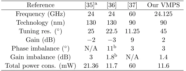
Table 4. Performance comparison of VMPS.
Reference [35]a [36] [37] Our VMPS
Frequency (GHz) 24 24 60 24.125
Technology (nm) 130 130 90 90
Tuning res. (◦) 25 22.5 11.25 45
Gain (dB) −2 −3 9 2
Phase imbalance (◦) N/A 11b 3 3 Gain imbalance (dB) 3 1.8b N/A 1.4 Total power cons. (mW) 21.36 11.7 60 11.6 aSimulation results.
bRMS error.
3.5. Voltage-Controlled Oscillator
The VCO scheme, as shown in Figure 10(a), is the usual cross-coupled pair, M1-M2, that provides the proper negative resistance to the LC tank. To couple with the low voltage supply, the current tail has been replaced with an inductor, Ltail, which does not reduce the headroom for the cross-coupled pair, but keeps the current constant at high frequency. Source follower buffers are used to reduce the VCO load pulling. Frequency tuning is achieved by using CMOS varactors. The whole design is parasitic-driven because the interconnections have parasitic capacitances, and the inductor and the varactor have resistive losses. The varactor losses are mitigated by connecting them in series with fixed, low-value, metal-insulator-metal (MIM) capacitors so that the varactor losses are slightly coupled with the LC tank. The slight coupling also improves the oscillator phase noise because the high tuning ratio of the varactor (which set theKV CO) is reduced. The inductor is already optimized from the foundry with a thick metal layer. The parasitic capacitances are minimized by implementing a compact layout.
The measurement results, plotted in Figure 10(c) and Figure 10(d), show a frequency tuning range from 23.05 GHz to 23.93 GHz. The range is slightly (∼1%) lower than that of the ISM band because the effect of the parasitic is always underestimated in simulation, and needs to be compensated for in the next design iteration, likely by introducing a bank of switchable capacitors. The output power plot includes the cable losses of 6 dB therefore the oscillator on-chip power reaches −12 dBm. The power consumption is 10 mW at 1.2 V. The phase noise of the VCO has been measured by locking
Vtune Rtune
L VDD
M2 M1 Cs Cs
Rb R b
Vbias
L tail
M3 M4
Vp, buffer G G Vn,buffer G G C C Cvar Rvar Rvar Cvar 51 fF 391 pH
6.6 k Ω
2 k Ω 174 pH 2 k Ω
40 0.09 25.6 0.09 25.6 0.09 40 0.09 51 fF
6.6 k Ω 51 fF
51 fF
2 k Ω
23.9 23.7 freq (GHz) 0.4
0.1 0.3 0.6 0.8 23.6
24
23.8
0.5
0 0.2 0.7 0.9
V (V)
1.1 23.5 23.3 23.2 23.4 23.1 23 Freq P 1 1.2 -40 -60 -70 -30 -50 -80 -100 -110 -90 -120 1 K
100 10 K 100 K 1 M 10 M
P (dBc/Hz)
Frequency (Hz) noise tune (a) (b) (c) (d) out -13 -17 -19 -11 -15 -21 -23
P (dBm)
out
Figure 10. VCO schematic, die photo and measured results. (a) Cross-coupled VCO schematic.
Table 5. Performance comparison of 24 GHz VCO.
Reference [38] [38] [40] Our VCO
Frequency (GHz) 22.8 23.7 24.0 23.5
Technology (nm) 130 90 130 90
Tuning range (%) 13 7.2 5.8 4.2
Output power (dBm) 4 −1.2 6a −12
Phase noise (dBc/Hz) @ 1 MHz −97 −102 −102 −85c Phase noise (dBc/Hz) @ 2 MHz −102 N/A −112 −102c
Total power cons. (mW) 43 22b 64 10
aPower amplifier included. bQVCO.
cExternal PLL chip measurement set-up.
the VCO with an off-chip PLL (ADF4107 by Analog Devices). The PLL circuit, implemented on an auxiliary printed circuit board, also contains a frequency divider chip (HMC447 by Hittite) and an LNA chip (HMC519 by Hittite) in order to satisfy the frequency and input power requirements of the PLL chip. The loop filter, also off-chip, has a 3 dB bandwidth of 100 kHz since the comparison frequency is 1 MHz. The measured phase noise plotted in Figure 10(d) shows the typical noise shape of a PLL synthesizer with an in-band phase noise of about −60 dBc/Hz, which is mainly due to the high value of the division ratio between the carrier frequency and the comparison frequency. The out-band phase noise is only −85 dBc/Hz at 1 MHz offset because of the loop filter bandwidth (1 MHz falls within the transition bandwidth) that could not be narrowed in the measurement setup. The noise quickly drops to −102 dBc/Hz at 2 MHz and −113 dBc/Hz at 10 MHz offset. Table 5 shows the comparison of our work with the state of the art. Our VCO shows the lowest power consumption. In order to compare the phase noise, the values at 2 MHz offset can be extrapolated from cited works by scaling the 1 MHz value of 6 dB per octave. In this way the−102 dBc/Hz measured at 2 MHz is only 6 dB worse than the concurrent work which consumes more power.
4. FE SYSTEM BUDGET ANALYSIS
Based on the system architecture proposed in Section 2.4 and the functional blocks developed in Section 3, the following sections will focus on the gain, noise figure and power consumption budget analysis of the two working modes of the FE. Other parameters such as linearity and filter selectivity are not considered for this budgetary analysis, which aims to show the feasibility of the architecture more than the development of an accurate model. Indeed, the missing blocks of the architecture, such as active I/Q mixers, a differential combiner, a PLL, an ADC, an IF amplifier and a tunable IF filter, are selected from the open literature and their parameters are used in the calculations.
4.1. Budget Analysis of the Doppler Radar Sensor Mode
When the FE works as a Doppler radar sensor, the block diagram in Figure 11 can be considered. The blocks selected from the open literature are tagged with the reference number between brackets while the blocks that have been implemented in this work are tagged with the name used in the previous sections and the parameters noted are the measured parameters.
First, the gain budget can be calculated. The necessary total receiver gain is estimated by the equation:
GRX(dB) =GRF +GIF = 20 logVADC,RMS
VR,radar ,
(5)
3-stage LNA G: 18.6 dB NF: 5.5 dB
I/Q Mixer G:1dB NF: 9 dB
2 × [42]
OTA G: 20 dB
[43]
3-stage LNA G: 18.6 dB NF: 5.5 dB
I/Q Mixer G:1dB NF: 9 dB
2 × [42]
IF amp. LPF G: 60 dB
[44]
ADC [41] I/Q 2 ×
VCO Pout: -12 dBm
PLL [45] VMPS
G: 2 dB
VMPS G: 2 dB 3-stage
LNA G: 18.6 dB NF: 5.5 dB
1-stage LNA G: 6.7 dB
1-stage LNA G: 6.7 dB
3-stage LNA G: 18.6 dB NF: 5.5 dB 4-channel
4 × 4×
4-channel
4 × RX
Antenna Array
TX Antenna
Array
Figure 11. Block diagram in Doppler radar sensor mode.
The ADC block is taken from [41]. In this work, the full-scale range is 120 mV peak to peak. Meanwhile, the receiving power of the radar sensor is estimated by Eq. (2), which is rewritten:
PR,radar=PT X+CP GT X+GT X−P Lradar+GRX −LM
=1 dBm + 12 dB + 16.7 dB−152 dBm + 16.7 dB−10 dB≈ −116 dBm. (6) The calculated received power, i.e., −116 dBm, corresponds to 0.35µV on 50 Ω. Thus, the voltage gain of the receiver path can be calculated by Eq. (5), which gives around 102 dB. The total receiver gain is the sum of the gain from the RF path (GRF) and from the IF path (GIF). The gain of the RF path has the contribution from one three-stage LNA, one mixer, one combiner and the coherent receiver process gain. The three-stage LNA can provide 18.6 dB of gain and 5.5 dB of NF. The specifications of the I/Q mixer can be selected from [43], which shows 1 dB of gain and 9 dB of NF. Four channels can be combined by an operational transconductance amplifier (OTA) with 20 dB of voltage gain [43]. The coherent addition provides 12 dB of signal gain according to the discussion in Section 2.1. Therefore, the IF path needs to provide a gain of: GIF = 102−18.6−1−20−12≈50 dB.
The IF amplifier and low-pass filter can be selected from [44], which shows an IF VGA tunable gain from 18 dB to 60 dB, a tunable low-pass bandwidth up to 32 MHz and a power consumption of 0.7 mW. The ADC in [41] is a five-bit flash ADC with 20 MHz of bandwidth and 28 mW of power consumption. The gain budget in the LO path concerns the input LO power requirement of the active mixer, i.e., −3 dBm. The output power of the proposed VCO is−12 dBm. Therefore, after the VMPS gain of 2 dB, it still needs the gain of a single-stage LNA, i.e., almost 7 dB.
By applying the Friis formula to the blocks cascaded, a single-channel NF of 6 dB is worked out. This matches the desired value used in the radar range estimation in Section 2.1, which results in 60 meters of range.
In the transmitter path, the continuous-wave signal needs to be amplified before the antenna array. After the VMPS, the output power of the signal is−10 dBm. So it still needs an amplifier circuit used as a power amplifier, for example, one three-stage LNA, who has 18.6 dB gain and consumes 18 mW. The extra gain can be desired for the compensation of process-voltage-temperature variation, maybe adjusting the bias point for gain regulation.
Table 6. Power consumption budget calculation of the Doppler radar sensor mode.
Block Quantity Unit Pow.
(mW)
Summed Pow. (mW)
Tot. Pow. (mW)
Receiver Path
3-stage LNA 4 18 72
195.9
I/Q mixer [42] 8 6.9 55.2
Combiner [43] 1 12 12
IF amplifier & filter [44] 2 0.35 0.7
ADC [41] 2 28 56
LO Path
VCO 1 10 10
107.3
PLL [46] 1 33.3 33.3
VMPS 4 11.7 46.8
1-stage LNA 4 4.3 17.2
Transmit Path 3-stage LNA 4 18 72 72
Total 375
3-stage LNA G: 18.6 dB NF: 5.5 dB
I/Q Mixer G: 1 dB NF: 9 dB 2 × [42]
OTA G: 20 dB
[43]
IF amp. LPF G: 60 dB
[44]
ADC [41] I/Q 2 ×
VCO Pout:
-12 dBm
PLL [45] VMPS
G: 2 dB
VMPS G: 2 dB 1-stage
LNA G:6.5dB
3-stage LNA G: 18.6 dB NF: 5.5 dB RX
Antenna Array
TX Antenna
Array
Figure 12. Block diagram in transceiver mode.
4.2. Budget Analysis of the Transceiver Mode
With the same methodology, the budget analysis of the transceiver mode is carried out. Figure 12 shows the block diagram of the components used in this working mode.
The gain budget of the receiving path is considered first. Recalling that the receiver sensitivity is
−85 dBm (17.7µV on 50 Ω) and the ADC full-scale is 120 mVP P, the receiver total voltage gain has to be approximately 68 dB. This can be achieved by using the same IF amplifier/filter already seen for the radar mode provided that the IF bandwidth is properly tuned so that both modes can work properly by sharing the hardware. As shown in Eq. (7), the receiver sensitivity is lower than for the radar mode because the IF bandwidth is wider, and the coherent gain does not appear because the Ph-A is not used.
PR,com.=PT X,com.+GT X,com.−P Lcom.+GRX,com.−LM
Table 7. Power consumption budget calculation of the transceiver mode.
Block Quantity Unit Pow.
(mW)
Summed Pow. (mW)
Tot. Pow. (mW)
Receiver Path
3-stage LNA 1 18 18
100.5
I/Q mixer [42] 2 6.9 13.8
Combiner [43] 1 12 12
IF amplifier & filter [44] 2 0.35 0.7
ADC [41] 2 28 56
LO Path
VCO 1 10 10
71
PLL [45] 1 33.3 33.3
VMPS 2 11.7 23.4
1-stage LNA 1 4.3 4.3
Transmit Path 3-stage LNA 1 18 18 18
Total 189.5
Table 8. Summarized front-end performance estimations in two working modes.
Reference Doppler radar mode Transceiver mode
GRX (dB) 102 68
NF (nm) 6 6
Sensitivity (dBm) −82 −85
PT X (dBm) 7 1
SNRRX (dB) 12 12
Range (m) 60 140
Power (mW) 375 190
Hence, the selected IF amplifier and LPF are reusable. Since all the assumptions made in the range calculation are valid, the calculated range of 140 meters in Section 2.1 is confirmed.
Similarly, the transmission path is just one channel of the radar array and therefore the same amplification (i.e., one three-stage LNA) is necessary to increase the power of the BPSK signal generated by the VMPS to the 1 dBm of the desired transmitted power.
Table 7 shows the power breakdown of the transceiver mode. The total power is about 190 mW.
5. CONCLUSIONS
the open literature.
Table 8 shows the summarized performance calculations for both working modes. They are achieved with 190 mW and 375 mW of power consumption in transceiver and radar modes respectively. These are state of the art results for a 24 GHz Ph-A FE that combines Doppler radar and transceiver functionalities. To the authors’ knowledge, this Doppler radar FE is unique, and can become the basic node of a future WSN for smart lighting systems and intelligent transportation infrastructures.
ACKNOWLEDGMENT
The authors are grateful to the Swiss National Science Foundation (http://www.snsf.ch) who supported this work under grants 200020 127222/1 and 200021 146765/1.
REFERENCES
1. European Commission Directorate-General Communications Networks, Contents & Technology, “Lighting the cities: Accelerating the deployment of innovative lighting in European cities,” Report, http://ec.europa.eu, 2013.
2. The Zigbee Alliance, 2012.
3. Benet, G., F. Blanes, J. E. Sim´o, and P. P´erez, “Using infrared sensors for distance measurement in mobile robots,”Robotics and Autonomous Systems, Vol. 1006, 1–12, Elsevier, 2002.
4. EnLight Project, http://www.enlight-project.eu/en/home/, EnLight, 2011.
5. Wang, Z., P. Li, R. Xu, and W. Lin, “A compact X-band receiver front-end module based on low temperature co-fired ceramic technology,” Progress In Electromagnetics Research, Vol. 92, 167–180, 2009.
6. Cui, B., C. Wang, and X.-W. Sun, “Microstrip array double-antenna (MADA) technology applied in millimeter wave compact radar front-end,”Progress In Electromagnetics Research, Vol. 66, 125– 136, 2006.
7. ETSI, “ETSI EN 302 858-1 electromagnetic compatibility and radio spectrum matters (ERM),” ETSI 1.2.1, 2011.
8. Federal Communications Commission, http://www.fcc.gov/oet/spectrum/table/fcctable.pdf, FCC, 2010.
9. Gresham, I., A. Jenkins, R. Egri, C. Eswarappa, F. Kolak, R. Wohlert, J. Bennett, and J.-P. Lanteri, “Ultra wide band 24 GHz automotive radar front-end,” IEEE MTT-S International Microwave Symposium Digest, Vol. 1, 369–372, 2003.
10. Ragonese, E., A. Scuderi, V. Giammello, E. Messina, and G. Palmisano, “A fully integrated 24 GHz UWB radar sensor for automotive applications,” IEEE International Solid-State Circuits Conference — Digest of Technical Papers, (ISSCC), 306–307, 2009.
11. Notten, M., H. Veenstra, E. van der Heijden, G. Dolmans, and F. Jansen, “Antenna and flip-chip circuit board design for a 24 GHz short-range radar transceiver,” IEEE MTT-S International Microwave Symposium Digest, 1155–1158, 2008.
12. Ghazinour, A., P. Wennekers, J. Schmidt, Y. Yin, R. Reuter, and J. Teplik, “A fully-monolithic SiGe-BiCMOS transceiver chip for 24 GHz applications,” Proceedings of the Bipolar/BiCMOS Circuits and Technology Meeting, 181–184, 2003.
13. Lee, S., C.-Y. Kim, and S. Hong, “A K-band CMOS UWB radar transmitter with a bi-phase modulating pulsed oscillator,” IEEE Transactions on Microwave Theory and Techniques, Vol. 60, 1405–1412, 2012.
14. Kim, C., P. Park, D.-Y. Kim, K.-H. Park, M. Park, M.-K. Cho, S. J. Lee, J.-G. Kim, Y. S. Eo, J. Park, D. Baek, J.-T. Oh, S. Hong, and H.-K. Yu, “A CMOS centric 77 GHz automotive radar architecture,” IEEE Radio Frequency Integrated Circuits Symposium (RFIC), 131–134, 2012. 15. Infineon Technologies, “BGT24MTR11, silicon germanium 24 GHz transceiver MMIC,” Datasheet,
16. Wang, B., G. Tasselli, C. Botteron, and P.-A. Farine, “System design of a 24 GHz phased-array front-end for low-power applications,” Conference on Ph.D. Research in Microelectronics Electronics (PRIME), 1–4, 2012.
17. Tasselli, G., B. Wang, S. Ghamari, C. Robert, C. Botteron, and P.-A. Farine, “Development of a versatile low-power 24 GHz phased array front-end in 90 nm CMOS technology,”IEEE International NEWCAS Conference, 465–468, 2012.
18. Wang, B., G. Tasselli, C. Botteron, and P.-A. Farine, “24 GHz LNA and vector modulator phase shifter for phased-array receiver in CMOS technology,” IEEE International Symposium on Phased Array Systems and Technology (ARRAY), 89–92, 2013.
19. Alimenti, F., F. Placentino, A. Battistini, G. Tasselli, W. Bernardini, P. Mezzanotte, D. Rascio, V. Palazzari, S. Leone, A. Scarponi, N. Porzi, M. Comez, and L. Roselli, “A low-cost 24 GHz Doppler radar sensor for traffic monitoring implemented in standard discrete-component technology,” European Microwave Conference (EuMW), 1441–1444, 2007.
20. Radetsky, L., “Streetlights for local roads,” National Lighting Product Information Program NLPIP, 28 Pages, 2011.
21. Silver, S. and H. M. James,Microwave Antenna Theory and Design, McGraw-Hill Book Company, Inc., 1949.
22. Roselli, L., F. Alimenti, M. Comez, V. Palazzari, F. Placentino, N. Porzi, and A. Scarponi, “A cost driven 24 GHz Doppler radar sensor development for automotive applications,” European Microwave Conference (EuMW), 335–338, 2005.
23. Richards, M. A., J. A. Scheer, and W. A. Holm, Principles of Modern Radar: Basic Principles, SciTech Publishing, 2010.
24. Fortuny-Guasch, J. and J.-M. Chareau, “Radar cross section measurements of pedestrian dummies and humans in the 24/77 GHz frequency bands,” European Commission, Joint Research Centre, Institute for the Protection and Security of the Citizen, 2013.
25. Issakov, V., Microwave Circuits for 24 GHz Automotive Radar in Silicon-based Technologies, Springer, 2010.
26. Hajimiri, A., “Mm-wave silicon ICs: Challenges and opportunities,” IEEE Custom Integrated Circuits Conference, (CICC), 741–747, 2007.
27. Natarajan, A., S. K. Reynolds, M.-D. Tsai, S. T. Nicolson, J.-H. C. Zhan, D. G. Kam, D. Liu, Y.-L. O. Huang, A. Valdes-Garcia, and B. A. Floyd, “A fully-integrated 16-element phased-array receiver in SiGe BiCMOS for 60-GHz,”IEEE Journal of Solid-State Circuits (JSSC), Vol. 46, No. 5, 1059–1075, 2011.
28. Proakis, J. G. and M. Salehi, Communication System Engineering, Prentice Hall, Upper Saddle River, New Jersey, 1994.
29. Dupuis, O., X. Sun, G. Carchon, P. Soussan, M. Ferndah, S. Decoutere, and W. De Raedt, “24 GHz LNA in 90 nm RF-CMOS with high-Q above-IC inductors,” IEEE European Solid-State Circuits Conference (ESSCIRC), 89–92, 2005.
30. Nguyen, G. D., Y. Chiu, and M. Feng, “24-GHz low noise amplifier using coplanar waveguide series feedback in 130-nm CMOS,”Asia Pacific Microwave Conference (APMC), 1148–1151, 2009. 31. Tsai, M.-H. and S. S. H. Hsu, “A 24 GHz low-noise amplifier using RF junction varactors for
noise optimization and CDM ESD protection in 90 nm CMOS,” IEEE Microwave and Wireless Components Letters (MWCL), Vol. 27, No. 7, 374–376, 2011.
32. Paramesh, J., R. Bishop, K. Soumyanath, and D. J. Allstot, “A four-antenna receiver in 90-nm CMOS for beamforming and spatial diversity,” IEEE Journal of Solid-State Circuits (JSSC), Vol. 40, No. 12, 2515–2524, 2005.
33. Wu, P.-S., H.-Y. Chang, M.-D. Tsai, T.-W. Huang, and H. Wang, “New miniature 15–20-GHz continuous-phase/amplitude control MMICs using 0.18-µm CMOS technology,”IEEE Transactions on Microwave Theory and Techniques, Vol. 54, No. 1, 10–19, 2006.
35. Kim, W.-G., J. P. Thakur, H.-Y. Yu, S.-S. Choi, and Y.-H. Kim, “Ka-band hybrid phase shifter for analog phase shift range extension using 0.13-µm CMOS technology,” IEEE International Symposium on Phased Array Systems and Technology (ARRAY), 603–606, 2010.
36. Koh, K. J. and G. M. Rebeiz, “0.13-µm CMOS phase shifters for X-, Ku-, and K-band phased arrays,” IEEE Journal of Solid-State Circuits (JSSC), Vol. 42, No. 11, 2535–2546, 2007.
37. Kim, K.-J. and K. H. Ahn, “Design of 60 GHz vector modulation based active phase shifter,”IEEE International Symposium on Electronic Design, Test and Application (DELTA), 140–143, 2011. 38. Hossain, M., U. Pursche, C. Meliani, and W. Heinrich, “High-efficiency low-voltage 24 GHz VCO in
130 nm CMOS for FMCW radar applications,”European Microwave Integrated Circuits Conference (EuMIC), 105–108, 2013.
39. Tormanen, M. and H. Sjoland, “A 24-GHz quadrature receiver front-end in 90-nm CMOS,”Asia Pacific Microwave Conference (APMC), 1152–1155, 2009.
40. Cao, Y., M. Tiebout, and V. Issakov, “A 24 GHz FMCW radar transmitter in 0.13µm CMOS,”
European Solid-State Circuits Conference (ESSCIRC), 498–501, 2008.
41. Malla, P., H. Lakdawala, K. Kornegay, and K. Soumyanath, “A 28 mW spectrum-sensing reconfigurable 20 MHz 72 dB-SNR 70 dB-SNDR DT Sigma-Delta ADC for 802.11n/WiMAX receivers,”IEEE International Solid-State Circuits Conference Digest of Technical Papers (ISSCC), 496–631, 2008.
42. Verma, A., L. Gao, K. O. Kenneth, and J. Lin, “A K-band down-conversion mixer with 1.4-GHz bandwidth in 0.13µm CMOS technology,” IEEE Microwave and Wireless Components Letters (MWCL), Vol. 15, No. 8, 493–495, 2005.
43. Shem-Tov, B., M. Kozak, and E. G. Friedman, “A high-speed CMOS OP-AMP design technique using negative Miller capacitance,” IEEE International Conference on Electronics, Circuits and Systems (ICECS), 623–626, 2004.
44. Deiss, A. and Q. Huang, “A low-power 200-MHz receiver for wireless hearing aid devices,” IEEE Journal of Solid-State Circuits (JSSC), Vol. 38, No. 5, 793–804, 2003.