Design of 4-bit Carry look Ahead Adder with
Low Area and Low Power
Alithi Jyothi 1, Earli Manemma 2 Bhaskara Rao Doddi3
P.G. Student, Dept. of Electronics & Communication Engineering, Visakha Engineering College, Narava, A.P, India1
Associate Professor, Dept. of Electronics & Communication Engineering, Visakha Engineering College, A.P, India2
Assistant Professor, Dept. of Electronics & Communication Engineering, Visakha Engineering College, A.P, India3
ABSTRACT: Adder has applications in digital signal processing to perform finite impulse response and infinite impulse response. In Ripple carry adder only when the previous Carry is known then only computation will happen for Sum and Carry, so Delay will be more is the disadvantage but area will be less. when compared to carry look ahead adder in which area will be the disadvantage but speed will be the advantage. Now we need to reduce the Area as well as Power. We are going to Design the Circuit in Transistor level and Aiming for Maximum Optimization. In this project the proposed Adder has been designed by using STATIC CMOS 180nm TECHNOLOGY and the tool being used is TANNER EDA tool.
KEYWORDS:8TCircuit , XnorCircuit , Generate, Propagate.
I. INTRODUCTION
Carry look ahead adder presented was designed by Amita in 2014, Implementation of Adder consumes more power as well as more Area but gives more speed[1]. Carry look ahead adders presented was designed by jagannath samanta in 2013, out of the many logic styles they have used they say the best design with transistor count is 146 for 4-bit and 452 for 8-bit[2]. K.Ueda employed carry look ahead adder by using pass transistor logic which by default has problem of logic level degradation[3]. Y.T Pai proposed a design for high speed but we are here interested in all the design constraints[4].
Now we need to design a carry look ahead adder by implementing our own technique such that functional behavior of the circuit should be correct but off course by keeping in mind the design constraints like AREA as well as POWER as these are our concern. We have designed carry look ahead adder by using STATIC CMOS logic style, it has advantage of easily being converted to a layout, because layout is the final implementation of the circuit and circuit is just symbolic representation. To achieve less transistor count
we can chose logic styles like PTL which by default takes less number of Transistors but we have chosen STATIC CMOS which by default takes more number of transistors but we need to design the carry look ahead adder which consumes more Area with less number of transistors. Logic style like PTL(Pass Transistor Logic) has disadvantage of less noise immunity as well as the problem of implementing in technology’s which has less supply voltages.
II. RELATEDWORK
ISSN(Online) : 2319-8753 ISSN (Print) : 2347-6710
I
nternational
J
ournal of
I
nnovative
R
esearch in
S
cience,
E
ngineering and
T
echnology
(An ISO 3297: 2007 Certified Organization)
Vol. 5, Issue 9, September 2016
Gate for Propagate and AND Gate for Generate and in General to have Optimized Circuit it should consist more of NOT,NOR and NAND Gates[1].
Carry lookahead adder was Designed by using Static style and the Technology used is 180nm which is the Channel length and the Design was developed at Gate level and they have used AND,OR and XOR Gates and their Maximum Fan-in is 5 and Fan-out is 4. Here is also the same case of using XOR for Propagate and AND for Generate which might not be affective[2].
Proposed Carry lookahead adder has Low Area and Low Power and design is Static and the Technology used is 180nm we have used NOR,NAND,XNOR and 8T Circuit as our Building blocks and their Maximum Fan-in is 3, Maximum Fan-out is 4 and the Design was developed at Transistor level which can give maximum Optimization since it is the Lowest level of Design abstraction.
III.CARRYLOOKAHEADADDER
Adder is going to add 4 bits of A(A3 to A0) and 4 bits of B(B3 to B0) and gives 5-bit result out of those 4-bits will be sum bits and 1-bit will be carry bit. we can design the circuit for Carry look ahead adder which by default gives high speed but at the cost of Area.
Now let us see how can we design the circuit for 4-bit carry look ahead adder coming from the least significant bit side that is A0 and B0, there will be Carry in. Now just a Xnor circuit is needed and it is a Two-Output Circuit in which first output is the Propagate output(p0) and second is the Generate output(G0). To achieve Propagate and Generate for the rest of bits that is P1,G1,P2,G2,P3,G3 Xnor circuit can be again used and now we are with all Generate and Propagate outputs.
Now to find out Carry output of Least Significant Bit that is c1 we require two 2-input Nand gates. Now to find out Carry output of (Least Significant+1)Bit that is c2 we require three 2-input Nor gates and one 2-input Nand gate. Now to find out Carry output of (Least Significant+2)Bit that is c3 we require two not gates, three 2-input Nor gates, one 3-input Nor gate and one 2-3-input Nand gate. Now to find out Carry output of Most Significant Bit that is c4 we require one 8TCircuit.
Now to find out Sum output of Least Significant Bit that is S0 we require one 2-input Xnor gate. Now to find out Sum output of (Least Significant+1)Bit that is S1 we require one 2-input Xnor gate. Now to find out Sum output of (Least Significant+2)Bit that is S2 we require one 2-input Xnor gate. Now to find out Sum output of Most Significant Bit that is S3 we require one 2-input Xnor gate.
There are 2 cells in this Carry look ahead adder named XNOR, 8T Circuit. XNOR has two inputs and two outputs and it takes 10 number of Transistors, 8T Circuit has four inputs and one output and needs 8 number of Transistors. Fig.1 shows a 8TCircuit which has four inputs and one output and it was needed to calculate the final Carry that is C4. Fig.2 shows a XNOR Circuit which has two inputs and two outputs and it was needed to find out the Generate and Propagate Outputs.
Fig.1 8T Circuit
Fig.1 shows a 8Transistor Circuit which has four inputs and one output and it was needed to calculate the final Carry that is C4. Out of the four inputs input2 corresponds to Propagate Output of the MSB bits, input3 corresponds to the Generate Output of the MSB bits, remaining are the previous Propagate and Generate Outputs. We can clearly Observe when Input3 is activated Low Output will be High.
ISSN(Online) : 2319-8753 ISSN (Print) : 2347-6710
I
nternational
J
ournal of
I
nnovative
R
esearch in
S
cience,
E
ngineering and
T
echnology
(An ISO 3297: 2007 Certified Organization)
Vol. 5, Issue 9, September 2016
Fig.2 shows a XNOR Circuit which has two inputs and two outputs and it was needed to find out the Generate and Propagate Outputs. Generate Output is Designed for Low and Propagate Output is also the same. This block is needed at every bit position from MSB to LSB.
Fig.3 Schematic of 4-bit CLA.
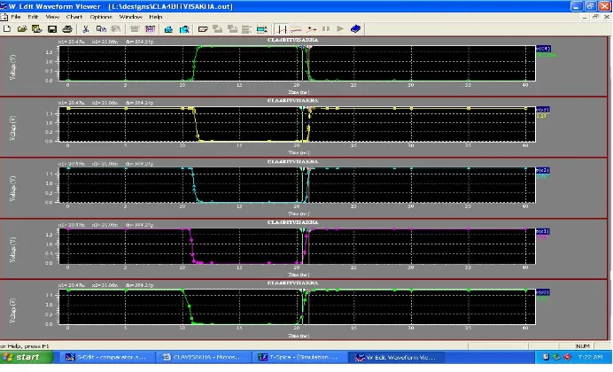
Fig.4 Delays for Low to High Carry outputs.
Fig.4 shows Delay comparisons of all the Carry Outputs C1,C2,C3 and C4. The worst Delay is for C4 and it is 0.14ns. It has been observed that Delay difference between all the Carry Outputs is less. Above Waveform has two Vertical Cursor Bars and the first one corresponds to Input changing 50% and Second one corresponds to Output changing 50%. Second Vertical Cursor Bar of C4 depicts Output reaching 0.9 volts.
Fig.5 Delays for High to Low Carry outputs
ISSN(Online) : 2319-8753 ISSN (Print) : 2347-6710
I
nternational
J
ournal of
I
nnovative
R
esearch in
S
cience,
E
ngineering and
T
echnology
(An ISO 3297: 2007 Certified Organization)
Vol. 5, Issue 9, September 2016
Fig.6 Delays for High to Low Sum outputs.
Fig.6 shows Delay comparisons between Sum outputs and the worst Delay is for S3 and it is 0.65ns.It has been observed that Delay difference between all the Sum Outputs is less. Vertical Cursor Bars are placed at the Output Transition of ‘1’ to ‘0’.
Fig.7 Delays for Low to High Sum outputs.
IV.TRANSISTORLEVELDESIGN
Any digital logic circuit can be designed in gate level or Transistor level, if we design the circuit in gate level maximum optimization is not possible because if we convert that circuit into Transistor level then overall Transistor count will be more leading to ineffective VLSI design constraints such as Power, Area and Speed. Though there is a common saying that low Area leads to low Cost, in Universal gates based design constraints like Area, Power and Delay will be increased but Cost may be reduced in assumption that already Nand or Nor IC is readily available.
We can design the circuits in Transistor level and if that circuit has only not, Nor, Nand, AOI(And-Or-Invert) and OAI(Or-And-Invert) then circuit has been optimized to some extent. In our design approach never we are interested in forming the equations, instead the conditions will be picked and that conditions will be translated into the circuit and how affectively that is being done that much the optimization will be achieved.
By using this Transistor level designing Chip Area can be minimized since less number of Transistors are required and Dynamic Power consumption also can be minimized because less number of Transistors will be ON and OFF. Coming to the Speed Constraint, Fan-in and Fan-Out has to be limited and even we can go for Transistor Sizing in which Transistor’s Width’s will be varied and this varied Transistors will offer more Speed if the Width is increased but at the expense of Area. The main purpose of Transistor Sizing is to make sure that Delay difference between Propagation of High-to-Low and Propagation of Low-to-High for the Output should be very less.
V. PERFORMANCEANALYSIS
Implementation of 4-bit Carry look ahead adder has been done using STATIC CMOS logic style which by default needs more number of Transistors.
TABLE1 AVERAGE POWER CONSUMPTION IN THREE DESIGNS
Table1 shows Power comparison of AMITA Carry look ahead adder (Reference1), JAGANNATH SAMANTA Carry look ahead adder(Reference2) and the proposed Carry look ahead adder.. This table clearly shows that proposed Carry look ahead adder has very less power dissipation that too in nano watts than reference2 as well as reference1.
TABLE2 COMPARISION OF AREA IN TWO DESIGNS 4-BIT Design in Reference1 (mW) Design in Reference2 (uW) Design in This paper (nW) Average Power
1.369 2.67 56.8
AREA (No.of Transistors)
Design in reference2
Design in this paper
ISSN(Online) : 2319-8753 ISSN (Print) : 2347-6710
I
nternational
J
ournal of
I
nnovative
R
esearch in
S
cience,
E
ngineering and
T
echnology
(An ISO 3297: 2007 Certified Organization)
Vol. 5, Issue 9, September 2016
The Carry look ahead adder which we designed using STATIC CMOS logic style uses less number of transistors which was shown in Table2. 96 number of Transistors were reduced only for 4-bit and in equal proportion reduction will be for N-bit.
VI. CONCLUSION
Carry look ahead adder is widely used where fast computation is needed especially in multipliers but disadvantage is Area will become worsen as size increases but we were able to design the circuit with less Area and since we have designed Adder using Carry look ahead approach by default we will achieve high speed and coming to the another important design constraint that is power by default STATIC CMOS logic, power consumption will be less.
All VLSI design constraints were achieved from our design. we came with our own Design it was possible because of the FULL-CUSTOM Design in which Circuit have to be designed from the Scratch in contrast with the Semi-Custom based design we need to write the code and then Synthesize the code and then get the netlist, so by default FULL-CUSTOM design offers best Optimization when compared to Semi-Custom design in which Optimization depends on the person who does the coding as well as the Tool which does the Synthesis.
REFERENCES
[1] Amita,”Design and analysis of carry look ahead adder using CMOS technique”. IOSR journal of electronics and communication Engineering: ISSN:2278-2834, vol-9,issue2(MAR-APR) 2014 pp-92-95.
[2] Jagannath samanta,”performance analysis of high speed low power Carry look ahead adder using different logic styles”. International journal Of soft computing and engineering(IJSCE) ISSN:2231-2307, vol-2,issue 6(JAN-2013) pp-330-336.
[3] K. Ueda, H. Suzuki, K. Suda, H. Shinohara, K. Mashiko,et.al “A 64-bit Carry Look Ahead Adder Using Pass .” IEEE Journal of Solid-Stale Circuits, vol. 31, no. 6 pp. 810-818, 1996.
[4] Y. T. Pai and Y. K. Chen., “The Fastest Carry Lookahead Adder.” IEEE, Proceedings of the Second IEEE International Workshop on Electronic Design, Test..
[5] Wei, B. W.; Thompson, C. D.; "Area-Time Optimal Adder Design", Computers, IEEE Transactions on, Vol. 39, No. May 1990, pp. 666-675. [6] Jan M. Rabaey, Anantha Chandrakasan, and Borivoje Nikolic, “Digital Integrated Circuits A Design Perspective,” Second Edition, Pearson Education, 2003.
[7] M.M. Mano, Digital Design. Englewood CLIFFS, NJ: Prentice-Hall, 1991,ch.5.
[8] N. West and K. Eshraghian, Principles of CMOS VLSI Design. Reading, MA: Addison-Wesley, 1993,ch.8.
[9] V. Kantabruta, A recursive carry-lookahead/carry-select hybrid adder, IEEE Transactions on Computers 42 (12) (1993) 1495–1499.