93 |
P a g e
www.ijarse.com
DESIGN OF CACHE SYSTEM USING BLOOM FILTER
ARCHITECTURE
1
R.Deepa,
2M. Brundha
1
PG Scholar, Department of ECE, Excel Engineering College, (India)
2
Assistant Professor, Department of ECE, Excel Engineering College, (India)
ABSTRACT
The cache is a crucial component for managing the memory wall problem. In particular, the L2 cache has
become increasingly popular in chips for high-end embedded systems such as smart phones and tablet PCs. The
cache size ranges from 256 kb to 1 MB and is expected to increase further to meet the ever-increasing bandwidth
requirements of high-end applications, e.g., 3-D graphics-based user interfaces. The ever-growing usage and large
area of the L2 cache result in significant power consumption. Tag comparison in a highly associative cache
consumes a significant portion of the cache energy. Existing methods for tag comparison reduction are based on
predicting either cache hits or cache misses. This project introduce the new idea for both cache hit and miss
predictions. Here a partial tag- enhanced Bloom filter to improve the accuracy of the cache miss prediction
method and hot/cold checks that control data liveness to reduce the tag comparisons of the cache hit prediction
method.
Keywords : Cache, Low Power, Write-Through Policy, Bloom Filter.
I INTRODUCTION
Multi-Level on-chip cache systems have been widely adopted in high-performance microprocessors. To keep
data consistence throughout the memory hierarchy, write-through and write-back policies are commonly employed.
Under the write-back policy, a modified cache block is copied back to its corresponding lower level cache only
when the block is about to be replaced. While under the write-through policy, all copies of a cache block are
updated immediately after the cache block is modified at the current cache, even though the block might not be
evicted. As a result, the write-through policy maintains identical data copies at all levels of the cache hierarchy
throughout most of their life time of execution. Many high performance microprocessors employ cache
write-through policy for performance improvement and at the same time achieving good tolerance to soft errors in
on-chip caches. However, write-through policy also incurs large energy overhead due to the increased accesses to
caches at the lower level (e.g., L2 caches) during write operations. Here a new cache architecture referred to
94 |
P a g e
www.ijarse.com
the way tags of L2 cache in the L1 cache during read operations, the proposed technique enables L2 cache to work
in an equivalent direct-mapping manner during write hits, which account for the majority of L2 cache accesses.
This leads to significant energy reduction without performance degradation. Simulation results on the SPEC
CPU2000 benchmarks demonstrate that the proposed technique achieves 65.4% energy savings in L2 caches on
average with only 0.02% area overhead and no performance degradation. Similar results are also obtained under
different L1 and L2 cache configurations. Furthermore, the idea of way tagging can be applied to existing
low-power cachedesign techniques to further improve energy efficiency.
1.1
Uses Of Write Through Policy
Under the write-through policy, caches at the lower level experience more accesses during write operations.
Obviously, the write-through policy incurs more write accesses in the L2 cache, Power dissipation is now
considered as one of the critical issues in cache design. Here new cache architecture, referred to as c o u n t i n g
b l o o m f i l t e r c a c h e s ys t e m , to improve the energy efficiency of write-through cache systems with minimal
area overhead and no performance degradation. Consider a two-level cache hierarchy, where the L1 data cache is
write-through and the L2 cache is inclusive for high performance. It is observed that all the data residing in the L1
cache will have copies in the L2 cache. In addition, the locations of these copies in the L2 cache will not
change until they are evicted from the L2 cache. Thus, we can attach a tag to each way in the L2 cache and send
this tag information to the L1 cache when the data is loaded to the L1 cache. By doing so, for all the data in the
L1 cache, we will know exactly the locations (i.e., ways) of their copies in the L2 cache. During the subsequent
accesses when there is a write hit in the L1 cache (which also initiates a write access to the L2 cache under the
write-through policy), we can access the L2 cache in an equivalent direct-mapping manner because the way tag of
the data copy in the L2 cache is available. As this operation accounts for the majority of L2 cache accesses in most
applications, the energy consumption of L2 cache can be reduced significantly.
1.2 Counting Bloom Filter (CBF)
An increasing number of architectural techniques have relied on hardware counting bloom filters (CBFs) to
improve upon the energy, delay, and complexity of various processor structures. CBFs improve the energy and speed
of membership tests by maintaining an imprecise and compact representation of a large set to be searched. This
paper studies the energy, delay, and area characteristics of two implementations for CBFs using full custom layouts
in a commercial 0.13- m fabrication technology. One implementation, S-CBF, uses an SRAM array of counts and a
shared up/down counter. Our proposed implementation L-CBF, utilizes an array of up/down linear feedback shift
registers and local zero detectors. Circuit simulations show that for a 1 K-entry CBF with a 15-bit count per entry,
L-CBF compared to S-CBF is 3.7 or faster and requires 2.3 or 1.4 less energy depending on the operation.
95 |
P a g e
www.ijarse.com
energy and delay of various CBF organizations during architectural level explorations when a physical level
implementation is not available.
For example, CBFs have been used to improve performance and power in snoop-coherent multiprocessor or
multi-core systems. CBFs have been also utilized to improve the scalability of load/store scheduling queues and to reduce
instruction replays by assisting in early miss determination at the L1 data cache. In these applications, CBFs help
eliminate broadcasts over the interconnection network in multi- processor systems; CBFs also help reduce accesses
to much larger and thus much slower and power-hungry content addressable memories, or cache tag arrays.
In all aforementioned hardware applications, CBFs improve the energy and speed of membership tests. Checking
whether a memory block is currently cached is an example of a member- ship test in processors. The CBF provides
a definite answer for most, but not necessarily for all, membership tests. As such, the CBF does not replace entirely
the underlying conventional mechanism (e.g., cache tags), but it dynamically bypasses the conventional
mechanism, which can be slow and power hungry, as frequently as possible.
Accordingly, the benefits obtained through the use of CBFs depend on two factors. The first factor is how
frequently a CBF can be utilized. Architectural techniques and application behavior determine how many
member- ship tests can be serviced by the CBF. The second factor is the energy and delay characteristics of the
CBF. The more member- ship tests are serviced by the CBF “alone” and the more speed and energy efficient the
CBF implementation is, the higher the benefits.
1.3
Process of Read and Write in cache
Whenever a data is updated in the L1 cache, the L2 cache is updated with the same data as well. This results in
an increase in the write accesses to the L2 cache and consequently more energy consumption
.
The L1 cachewhere read operations ac- count for a large portion of total memory accesses, write operations are dominant in the L2
cache for all but three benchmarks (galgel, ammp, and art). This is because read accesses in the L2 cache are
initiated by the read miss in the L1 cache, which typically occur much less frequently.
Hence it reducing the energy consumption of L2 write accesses is an effective way for memory power
management. Note that the proposed technique does not change the cache replacement policy. When a cache
line is evicted from the L2 cache, the status of the cache line changes to “invalid” to avoid future fetching and
thus prevent cache coherence issues.
Since way-tag arrays will be accessed only when a data is written into the L1 data cache (either when CPU
updates a data in the L1 data cache or when a data is loaded from the L2 cache), they are not affected by
96 |
P a g e
www.ijarse.com
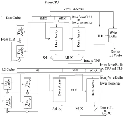
Fig. 1. Illustration of the Conventiona1 Cache System
II BLOOM FILTER PROCESS
The binary Bloom filter is an M-bit vector, with initially set to 0. There are two actions available:
programming and query. When programming an element ai in set P , the k bit positions (in the M-bit vector)
indexed by the k hash functions are set to 1. On a query on an element aj , if all of the bits in the M-bit
vector indexed by the k hash functions have values of 1, then the query result is positive (likely existence).
Otherwise, the result is negative (definite nonexistence).
The Bloom filter is utilized to check the approximate nonmembership of a set. When applied to reducing tag
comparisons, each cache way is equipped with a Bloom filter. A query to the B l o o m filter (e.g., “is
address 0×100 in thecache way?”) gives either of two results: negative (definite nonexistence) and positive
(likely existence).
Note that a negative result from the Bloom filter guarantees nonexistence, i.e., a cache way miss. Thus, before the
tag structure in each cache way is accessed, first the Bloom filter per cache way is looked up. If the Bloom filter
indicates nonexistence, then tag comparison for the cache way is avoided, thereby saving the energy that would
have been consumed in tag comparison. Both: 1) the smaller energy consumed to access the Bloom filter
rather than the tag; and 2) the high prediction accuracy for cache way misses reduce the energy consumed in tag
comparison. For instance, in the case of a cache way miss, using the Bloom filter produces a net energy gain
as long as the following relationship holds:
EB < p × ET
97 |
P a g e
www.ijarse.com
respectively,2 and p is the cache miss prediction accuracy of the Bloom filter (= number of negative
results/number of total cache way misses).
The Bloom filter is described as follows. Assume a set P = {a1, a2, . . . , aN } of N elements (P corresponds to
a cache way and N is the number of tags in the cache way) and k distinct hash functions, each of which takes
ai as the input and outputs an index of log2 M bits as the result.
The programming of a binary Bloom filter corresponds to the cache line-fill. When a new cache line starts to
reside in a cache way, the Bloom filter associated with the cache way is programmed with the tag of the new
cache line. The query corresponds to a cache access for reading or writing. The Bloom filter can give a positive
result, i.e., likely existence, even in the case of a cache miss, which is called a false positive.
2.1
S-CBF:SRAM-Based CBF Implementation
CBF implementation consisting of an SRAM array of counts, a shared up/down counter, a zero- comparator, and a
small controller. We will refer to this implementation as S-CBF. The architecture of S-CBF is depicted in Fig. 2.
Updates are implemented as read-modify-write sequences asfollows: 1) the count is read from the SRAM; 2) it
is
adjusted
using the counter; and 3) it is written back to the SRAM. The probe operation is implemented as a readfrom the SRAM, and a compare with zero using the zero-comparator. A small controller coordinates this sequence of
actions.
Fig. 2. S-CBF architecture: an SRAM hold
In this optimization was proposed to speedup probe operations and to reduce their power. Specifically, an extra bit
Z is added to each count. When the count is nonzero the Z is set to false and when the count is zero, the Z is set
to true. Probes can now simply inspect Z. The Z bits can be implemented as a separate SRAM structure which is
98 |
P a g e
www.ijarse.com
architectures.
2.2
LFSRs
A maximum-length-bit LFSR sequences through states. It goes through all possible code permutations except
one. The LFSR consists of a shift register and a few embedded XNOR gates fed by a feedback loop. Each LFSR
has the following defining parameters:
i. Width, or size, of the LFSR (it is equal to the number of bits in the shift register);
ii. Number and positions of taps (taps are special locations in the LFSR that have a connection with the
feedback loop);
iii. Initial state of the LFSR which can be any value except one (all ones for XNOR feedback).
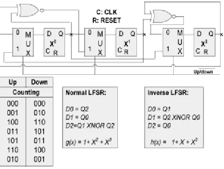
Without the loss of generality, we restrict our attention to the Galois implementation of LFSRs. State transitions
proceed as follows. The non-tapped bits are shifted from the previous position. The tapped bits are XNOR with
the feedback loop before being shifted to the next position. The combination of the taps and their locations can be
represented by a polynomial. Fig. 3 shows an 8-bit maximum-length Galois LFSR, its taps, and polynomial.
Fig. 3. Eight-bit Maximum-Length LFSR.
Fig. 4. Three-Bit Maximum-Length Up/Down LFSR.
The superposition of the two LFSRs (the original and its re- verse) forms a reversible “up/down” LFSR. The
up/down LFSR consists of a shift register similar to the one used for the unidi- rectional LFSR; a 2-to-1 multiplexer
per bit to control the shift direction; and twice as many XNOR gates as the unidirectional LFSR. Fig. 4 shows the
99 |
P a g e
www.ijarse.com
both up and down directions. In general, it is possible to construct a maximum-length up/down LFSR of any width
with two or six XNOR gates (i.e., four or eight taps) counters, has a delayof . Counters with a Manchester
carry-chain, carry lookahead and binary tree carry propagation have delay of though at the cost of
more energy and area. In applications where the count sequence is unimportant [e.g., pointers of circular
first-inputs–first-outputs (FIFOs) and frequency dividers], an LFSR counter offers a speed-power-area efficient
solution. The delay of an LFSR is nearly independent of its size. Specifically, the LFSR delay consists of a
flip-flop delay, an XNOR gate delay, and a feedback loop delay. The feedback loop delay is the propagation delay
of the last flip-flop output to the input of the furthest XNOR gate from the last flip-flop. Ignoring secondary
effects on the feedback path, the delay of an n-bit maximum length LFSR is O and independent of the
counter size. These characteristics make LFSRs a suitable counter choice for CBFs.
2.3
L-CBF Implementation
L-CBF includes a hierarchical decoder and a hierarchical output multiplexer. The core of the design is an array of
up/down LFSRs and zero detectors. The L-CBF design is divided into several partitions where each row of a
partition consists of an up/down LFSR and a zero detector.
L-CBF accepts three inputs and produces a single-bit output is-zero. The input operation select specifies the type of
operation: INC, DEC, PROBE, and IDLE. The input address specifies the address in question and the input reset is used
to initialize all LFSRs to the zero state. The LFSRs utilize two non-overlapping phase clocks generated internally from
an external clock.
We use a hierarchical decoder for decoding the address to minimize the energy-delay product. The decoder
consists of a pre-decoding stage, a global decoder to select the appropriate partition, and a set of local decoders,
one per partition. Each partition has a shared local is-zero output. A hierarchical multiplexer collects the local
is-zero signals and provides the single-bit is-zero output.
III IMPLEMENTATION
3.1
Partial Tag-Enhanced Bloom Filter
In case of a singleton entry, the original BF does not specify whether the incoming address is present in the cache
way. To be able to check the presence of the incoming address in thecase of a singleton
,
we propose the use ofa partial tag for each BF entry. Fig. 5 shows a partial tag-enhanced counting Bloom filter.
A BF entry has the tuple <C, Z, S, P>, where C is the counter, Z is the zero flag, S is the singleton flag,
and P is the partial tag. In our experiments, the size of the partial tag is small, 3 bits. Thus, compared to the
original Bloom filter, the partial tag-enhanced Bloom filter has an overhead of 4 bits (including the S flag) per
100 |
P a g e
www.ijarse.com
Fig. 5. Bloom Filter with a Partial Tag.
On each entry/exit (program/de-program) of address to/from the Bloom filter, the corresponding partial tag is
calculated in bitwise XOR operations as follows:
PTagnew = PTagold XOR PTagin //BF entry (program)
PTagnew = PTagold XOR PTagout //BF exit (de-program)
where PTagold and PTagnew represent the old and newly calcu- lated partial tags, respectively.
PTagin and PTagout represent the partial tags of the incoming (i.e., newly fetched) and outgoing (i.e., evicted)
cache lines, respectively. Such a partial tag manipulation gives the partial tag of the currently existing address
inthe case of a singleton entry.
For instance, assume that a BF entry has the following sequence of entries and exits: A1− in, A3−in, A5−in,
A3−out, A2−in, A1−out, and A5 out. After the exit of the last address A5, the corresponding BF entry
becomes a singleton entry because it contains only one address, i.e., A2, and its partial tag contains that of A2,
which is the only existing address are “1”.
Fig. 6: Partial Tag-Enhanced Bloom Filter Operation.
Fig. 6 shows a pseudo code of the partial tag-enhanced Bloom filter operation when k = 1 Compared to the
101 |
P a g e
www.ijarse.com
(lines 3–5 and 10– 11). If the counter of the corresponding BF entry is not zero, then the singleton check and
partial tag match are performed. If there is a mismatch between the partial tags of singleton entry and the
incoming address, the access is a miss for the corresponding way.
In the singleton cases where the partial tag comparison gives a match and in non singleton cases, subsequent
tag comparison needs to be performed (“likely hit” case in line 5). Note that when multiple (k > 1) hash functions
are used, if all the Bloom filter entries hashed by the k hash functions are singletons, all the singleton entries give
the same partial tag. Thus, in the case of multiple hash functions, the singleton test in line 4 checks to see if all the
k S flags.
IV CONCLUSION
In this project a multistep tag comparison method to reduce the energy consumed in tag comparison within
highly associative L2 caches. We presented a partial tag-enhanced Bloom filter to improve the accuracy of
cache miss prediction. We also explained hot/cold checks (with dynamic timeout tracking) as a cache hit
prediction method. To further reduce tag comparisons, a partial tag comparison that takes place during cold
checks. Finally, a method to determine the tradeoff between energy consumption and performance, which will be
particularly useful for latency- critical programs. The proposed method reduces the total cache energy consumption
by 8.86% as compared to existing methods and by 10.07% when zero awareness is applied. In future, we will
investigate the effectiveness of the proposed method in multicore environments.
REFERENCES
[1] A. Malik, B. Moyer, and D. Cermak, “A low power unified cache architecture providing power and
performance flexibility,” in Proc. Int. Symp. Low Power Electron. Design, IEEE January 2011..
[2] K. Osada, K. Yamaguchi, and Y. Saitoh, “SRAM immunity to cosmic-ray-induced multierrors based on
analysis of an induced parasitic bipolar effect,” IEEE J. Solid-State Circuits, May 2009
[3] J. Dai and L. Wang, “Way-tagged cache: An energy efficient L2 cache architecture under write through policy,”
in Proc. Int. Symp. Low Power Electron. Design, IEEE, March 2010.
[4] R. Min, W. Jone, and Y. Hu, “Phased tag cache: An efficient low power cache system,” in Proc. Int. Symp.
Circuits System, IEEE, June 2009.
[5] A. Moshovos, G. Memik, B. Falsafi, and A. Choudhary, “Jetty: Filtering snoops for reduced energy
consumption in smp servers,” in Proc. Ann. Int. Conf. High-Performance Comput. Arch.,
[6] P. Alfke, “Efficient shift registers, LFSR counters, and long pseudo- random sequence generators,” Xilinx,
102 |
P a g e
www.ijarse.com
[7] B. S. Amrutur, “Design and analysis of fast low power SRAMs,” Ph.D. dissertation, Elect. Eng. Dept., Stanford
Univ., Stanford, CA.
[8] M. Mamidipaka, K. Khouri, N. Dutt, and M. Abadir, “Analytical models for leakage power estimation of
memory array structures,” in Proc. Int. Conf. Hardw./Softw. Co-Design Syst. Synth.
[9] X. N. Chen and L. S. Peh, “Leakage power modeling and optimization of interconnection network,” in Proc.
Int. Symp. Low Power Electron. Des.
[10]T. Ishihara and F. Fallah, “A way memoization technique for reducing power consumption of caches in