Scholarship at UWindsor
Scholarship at UWindsor
Electronic Theses and Dissertations Theses, Dissertations, and Major Papers
2011
The Optical Response of Hydrogenated Amorphous Silicon
The Optical Response of Hydrogenated Amorphous Silicon
Jasmin Thevaril
University of Windsor
Follow this and additional works at: https://scholar.uwindsor.ca/etd
Recommended Citation Recommended Citation
Thevaril, Jasmin, "The Optical Response of Hydrogenated Amorphous Silicon" (2011). Electronic Theses and Dissertations. 440.
https://scholar.uwindsor.ca/etd/440
Hydrogenated Amorphous Silicon
by
Jasmin Joseph Thevaril
A Dissertation
Submitted to the Faculty of Graduate Studies
Through the Department of Electrical and Computer Engineering
In Partial Fulfillment of the Requirements for
The Degree of Doctor of Philosophy at the
University of Windsor
Windsor, Ontario, Canada
2011
c
Amorphous Silicon
by
Jasmin J. Thevaril
APPROVED BY:
Dr. J. Sabarinathan
University of Western Ontario
Dr. C. Rangan
Department of Physics
Dr. J. Wu
Department of Electrical with Computer Engineering
Dr. C. Chen
Department of Electrical with Computer Engineering
Dr. N. Kar
Department of Electrical with Computer Engineering
Dr. S. K. O’Leary
Department of Electrical with Computer Engineering
Dr. S. Das, Chair of Defense
Faculty of Graduate Studies
Previous Publication
I. Co-Authorship Declaration
I hereby declare that this thesis incorporates material that is the result of
research undertaken under the supervision of my supervisor, Dr. S. K. O’Leary.
Re-sults related to this research are reported in Chapters 2 through 6, inclusive.
I am aware of the University of Windsor’s Senate Policy on Authorship and I
certify that I have properly acknowledged the contributions of the other researchers
to my thesis, and I have obtained written permission from my co-author to include
the aforementioned materials in my thesis.
I certify that, with the above qualification, this thesis, and the research to
which it refers to, is the product of my own work.
II. Declaration of Previous Publication
This thesis includes 4 original papers that have been previously published/submitted
Chapter 2 The role that conduction band tail states play in determining the optical response of hydro-genated amorphous silicon, J. J. Thevaril and S. K. O’Leary, Solid State Communications, v 151, no. 7, pp. 730-733, 2011.
Published
Chapter 3 A dimensionless joint density of states formalism for the quantitative characterization of the optical response of hydrogenated amorphous silicon, J. J. Thevaril and S. K. O’Leary, Journal of Applied Physics,v 107, no. 8, pp. 083105-1-6, 2010
Published
Chapter 4 A universal feature in the optical absorption spec-trum associated with hydrogenated amorphous sil-icon: A dimensionless joint density of states anal-ysis, J. J. Thevaril and S. K. O’Leary, submitted toJournal of Applied Physics, on June 17, 2010.
Major
revi-sions required
Chapter 5 Defect absorption and optical transitions in hydro-genated amorphous silicon, J. J. Thevaril and S. K. O’Leary, Solid State Communications, v 150, no. 37-38, pp. 1851-1855, 2010
Published
I certify that I have obtained a written permission from the copyright owner(s) to include the above published materials in my thesis. I certify that the above
ma-terial describes work completed during my registration as a graduate student at the
University of Windsor.
I declare that, to the best of my knowledge, my thesis does not infringe upon
anyone’s copyright nor violate any proprietary rights and that any ideas, techniques,
quotations, or any other material from the work of other people included in my thesis,
published or otherwise, are fully acknowledged in accordance with standard
referenc-ing practices. Furthermore, to the extent that I have included copyrighted material
that surpasses the bounds of fair dealing within the meaning of the Canada Copyright
Act, I certify that I have obtained a written permission from the copyright owners to include such materials in my thesis.
I declare that this is a true copy of my thesis, including any final revisions, as
ap-proved by my thesis committee and the Graduate Studies office, and that this thesis
Through the use of a general empirical model for the density of states functions,
one that considers valence band band, valence band tail, conduction band band, and
conduction band tail electronic states, the sensitivity of the joint density of states
function to variations in the conduction band tail breadth, all other parameters being
held fixed at nominal hydrogenated amorphous silicon values, is examined. It is
found that when the conduction band tail is narrower than the valence band tail, its
role in shaping the corresponding spectral dependence of the joint density of states
function is relatively minor. This justifies the use of a simplified empirical model for
the density of states functions that neglects the presence of the conduction band tail
states in the characterization of the optical response.
A simplification of such an empirical model for the density of state functions
asso-ciated with hydrogenated amorphous silicon is then suggested, reducing the number
of independent modeling parameters from six to five as a result. As a consequence
of this simplification, it is found that one is able to cast joint density of states
eval-uations into a dimensionless formalism, this formalism providing an elementary and
effective platform for the determination of the underlying modeling parameters from
experiment. This simplification is justified by showing, for reasonable hydrogenated
amorphous silicon modeling parameter selections, that the joint density of states
acterization of the optical response associated with hydrogenated amorphous silicon,
a critical comparative analysis of a large number of different optical absorption data
sets is then considered. When these data sets are cast into this dimensionless
frame-work, a trend is observed that is almost completely coincident for all of the data
sets considered. This suggests that there is a universal character associated with the
optical absorption spectrum of hydrogenated amorphous silicon.
Finally, the role that defect states play in shaping the optical response of this
My supervisor, Dr. S. K. O’Leary, has enabled me to pursue my studies to the best
of my ability. His guidance and support have been unparallelled and I feel lucky to
have found such a great mentor. I would like to thank my supervisor. The scientific
approach and positive thinking that he has provided was a great base from which
to conduct my research. I am indebted to my supervisor for his support, patience,
guidance, and tons of hours of analysis and discussion of my research. I am sure that
everything I learned from him will be valuable throughtout my scientific career. I also
extend my sincerest gratitude towards my commitee members, Drs. C. Chen, N. Kar,
C. Rangan, and J. Wu, for their valuable guidance, encouragement, and leadership
throughout the course of this thesis. I am grateful to them for generously advising
me and for driving me on the right path towards the successful completion of this
thesis.
A special thank you to Dr. M. Ahmadi, the former Graduate Co-ordinator, Dr. X.
Chen, the Graduate Co-ordinator, Dr. M. A. Sid-Ahmed, the Department Head of
Electrical and Computer Engineering and Dr. J. Frank, the Dean of Graduate
Stud-ies, for mentoring me during the challenging times of my Ph.D studies.
Last, but most importantly, I want to thank my family for their support,
encour-agement, and patience. Mom, your unending love and encouragement kept me going
throughout my degree. My dad got me hooked into science and technology and
pro-vided me with invaluable advice, and allowed me to realize what I can achieve. My
husband, my son, and my brother, always encouraged me and taught me never to
Declaration of Co-Authorship / Previous Publication . . . iii
Abstract . . . v
Dedication . . . vii
Acknowledgements . . . viii
List of Tables . . . xii
List of Figures . . . xiii
List of Abbreviations and Symbols . . . xxiii
1 Introduction 1 1.1 Introduction to disordered semiconductors . . . 1
1.2 Distribution of atoms . . . 4
1.3 Device applications . . . 9
1.4 The optical response . . . 10
1.5 Distributions of electronic states . . . 14
1.6 Relation between the optical absorption spectrum and the DOS functions 19 1.7 Free electron density of states . . . 23
1.8 A review of empirical density of states models . . . 29
1.9 Modeling of the optical response . . . 40
1.10 Objective of this thesis . . . 53
1.11 Thesis organization . . . 56
References . . . 59
2 The sensitivity of the optical response of hydrogenated amorphous silicon to variations in the conduction band tail breadth 62 2.1 Introduction . . . 63
2.2 Analytical framework . . . 64
2.3 JDOS evaluation and analysis . . . 67
2.4 Conclusion . . . 75
References . . . 76
3.2 Modeling the distribution of electronic states . . . 82
3.3 JDOS formalism . . . 85
3.4 The imaginary part of the dielectric function . . . 89
3.5 The utility of the dimensionless JDOS formalism . . . 91
3.6 Conclusions . . . 94
References . . . 97
4 A universal feature in the optical absorption spectrum associated with hydrogenated amorphous silicon: A dimensionless joint density of states analysis 100 4.1 Introduction . . . 101
4.2 Modeling the optical response of a-Si:H . . . 102
4.3 The experimental data of Cody et al. . . 104
4.4 The experimental data of Viturro and Weiser and the experimental data of Reme˘s . . . 109
4.5 Critical comparative analysis . . . 116
4.6 Conclusions . . . 123
References . . . 124
5 Defect absorption and optical transitions in hydrogenated amor-phous silicon 128 5.1 Introduction . . . 129
5.2 Analytical framework . . . 131
5.3 Results . . . 134
5.4 Comparison with experiment . . . 140
5.5 Conclusions . . . 141
References . . . 144
6 Conclusions 148 References . . . 151
Appendix A Copyright Release - Journal of Applied Physics 152
Appendix B Copyright Release - Solid State Communications 154
1.1 The nominal DOS modeling parameter selections employed for the em-pirical DOS models described in this section. These modeling param-eters are representative of a-Si:H. . . 32
2.1 The nominal a-Si:H modeling parameter selections employed for the purposes of this analysis. These modeling parameters relate to Eqs. (2.5) and (2.6). . . 67
4.1 The model parameter selections corresponding to the fits to the exper-imental a-Si:H optical absorption data sets of Codyet al.[17] depicted in Figure 4.1. The number of excluded data points and the presence of a difference between the experimental results and the corresponding fits, for each data set considered, are also indicated. . . 106 4.2 The model parameter selections corresponding to the fits to the
exper-imental a-Si:H optical absorption data sets of Viturro and Weiser [27] depicted in Figure 4.3. The number of excluded data points and the presence of a difference between the experimental results and the cor-responding fits, for each data set considered, are also indicated. . . . 111 4.3 The model parameter selections corresponding to the fits to the
exper-imental a-Si:H optical absorption data sets of Reme˘s [28] depicted in Figure 4.5. The number of excluded data points and the presence of a difference between the experimental results and the corresponding fits, for each data set considered, are also indicated. . . 116
5.1 The nominal a-Si:H modeling parameter selections employed for the purposes of this analysis. . . 137 5.2 The a-Si:H modeling parameter selections employed for the purposes
1.1 A schematic depiction of the distribution of silicon atoms within c-Si and a-Si. The atoms are represented by the solid circles. The bonds are represented by the solid lines. The scale of the disorder within a-Si has been exaggerated for the purposes of illustration. . . 5 1.2 The coordination numbers associated each silicon atom in a
represen-tative sample of a-Si. The geometry has been exaggerated for the purposes of illustration. . . 7 1.3 A schematic representation of dangling bonds within a-Si. The atoms
are represented by the solid spheres. The dangling bonds are repre-sented by the dotted lines. The Si-Si bonds are reprerepre-sented by the solid lines. The ratio of the dangling bonds to the Si-Si bonds within a-Si has been exaggerated for the purposes of illustration. . . 8 1.4 The intensity of light as a function of the depth, z, from the surface
of the material, z = 0, for light normally incident on a material and propagating from the left, in the absence of reflection. . . 11 1.5 The spectral dependence of the optical absorption coefficient, α(~ω),
associated with hypothetical crystalline and amorphous semiconductors. 13 1.6 A schematic representation of the distributions of electronic states
as-sociated with a hypothetical amorphous semiconductor. . . 15 1.7 A schematic representation of the wavefunctions associated with
local-ized and extended electronic states. This figure is taken after Mori-gaki [25]. . . 16 1.8 The distributions of electronic states associated with a hypothetical
amorphous semiconductor. The conduction band and valence band mobility edges are depicted with the dashed lines. The defect states have been neglected. . . 18 1.9 The number of optical transitions allowed from a single-spin state in
experimental data points of Klazeset al. [27] are represented with the
solid points. . . 24
1.11 The representation of an electron confined within a cubic volume, of dimensions, L×L×L, surrounded by infinite potential barriers. . . . 26
1.12 The quantum numbers, nx, ny, and nz, shown in the first octet of three-dimensionaln-space. The density of such points is unity. . . 28
1.13 The empirical DOS model of Tauc et al. [30]. . . 31
1.14 The empirical DOS model of Chen et al.[31]. . . 33
1.15 The empirical DOS model of Redfield [32]. . . 35
1.16 The empirical DOS model of Cody [33]. . . 37
1.17 The empirical DOS model of O’Leary et al. [34]. . . 39
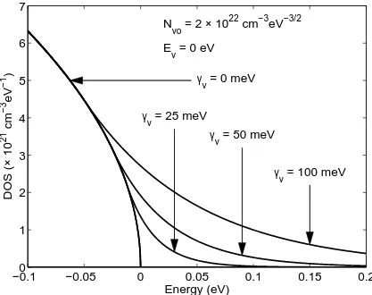
1.18 The valence band DOS function, Nv(E), for a number of selections of γv, plotted on a linear scale. This function, specified in Eq. (1.31) with EvT set to Ev− 1 2γv, is evaluated assuming the nominal DOS modeling parameter selectionsNvo = 2×1022 cm−3eV−3/2 and Ev = 0 eV for all cases. The abscissa axis represents the energy, E, while the ordinate axis depicts the corresponding valence band DOS value. . . 41
1.19 The valence band DOS function, Nv(E), for a number of selections of γv, plotted on a logarithmic scale. This function, specified in Eq. (1.31) with EvT set to Ev − 1 2γv, is evaluated assuming the nominal DOS modeling parameter selections Nvo = 2×1022 cm−3eV−3/2 and Ev = 0 eV for all cases. The abscissa axis represents the energy, E, while the ordinate axis depicts the corresponding valence band DOS value. 42 1.20 The conduction band DOS function,Nc(E), for a number of selections of γc, plotted on a linear scale. This function, specified in Eq. (1.32) with EcT set to Ec + 1 2γc, is evaluated assuming the nominal DOS modeling parameter selections Nco = 2×1022 cm−3eV−3/2 and Ec = 1.7 eV for all cases. The abscissa axis represents the energy, E, while the ordinate axis depicts the corresponding conduction band DOS value. 43 1.21 The conduction band DOS function, Nc(E), for a number of selec-tions of γc, plotted on a logarithmic scale. This function, specified in Eq. (1.32) withEcT set to Ec+ 1 2γc, is evaluated assuming the nominal DOS modeling parameter selections Nco = 2×1022 cm−3eV−3/2 and Ec = 1.7 eV for all cases. The abscissa axis represents the energy, E, while the ordinate axis depicts the corresponding conduction band DOS value. . . 44
all cases, the DOS modeling parameters are set to their nominal values tabulated in Table 1.1. . . 47 1.24 The valence band and conduction band DOS functions associated with
a-Si:H. The nominal DOS modeling parameter selections tabulated in Table 1.1 are employed for the purposes of this analysis. EvT is set to Ev− γ2v and EcT is set to Ec+
γc
2 for the purposes of this figure. The
critical energies, EvT and EcT, that separate the square-root distribu-tions from the exponential distribudistribu-tions, are clearly depicted. Repre-sentative VBB-CBB, VBB-CBT, VBT-CBB, and VBT-CBT optical transitions, are also shown. . . 50 1.25 The factors in the JDOS integrand, Nv(E) and Nc(E+~ω), and the
resultant product, Nv(E)Nc(E+~ω), for the case of ~ω set to 2.1 eV. The nominal DOS modeling parameter selections, tabulated in Table 1.1, are employed for the purposes of this analysis. Ranges of energy, corresponding to VBB-CBB, VBB-CBT, and VBT-CBB op-tical transitions, are depicted. VBT-CBT opop-tical transitions do not occur for this selection of~ω. This figure is taken after O’Leary [36]. 51 1.26 The factors in the JDOS integrand, Nv(E) and Nc(E+~ω), and the
resultant product, Nv(E)Nc(E+~ω), for the case of ~ω set to 1.4 eV. The nominal DOS modeling parameter selections, tabulated in Table 1.1, are employed for the purposes of this analysis. Ranges of energy, corresponding to VBB-CBT, VBT-CBB, and VBT-CBT op-tical transitions, are depicted. VBB-CBB opop-tical transitions do not occur for this selection of~ω. This figure is taken after O’Leary [36]. 52 1.27 The valence band and conduction band DOS functions associated with
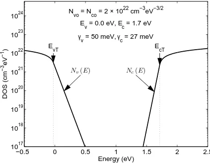
is determined assuming the nominal a-Si:H parameter selectionsNvo = 2×1022 cm−3eV−3/2, E
v = 0.0 eV, andγv = 50 meV. The conduction band DOS function,Nc(E), specified in Eq. (2.6), is determined assum-ing the nominal a-Si:H parameter selectionsNco= 2×1022cm−3eV−3/2, Ec= 1.7 eV, and γc = 27 meV. Only differences between the energies Ev and Ec will impact upon the obtained JDOS results. The critical points at which the band states and tail states interface,EvT and EcT,
are clearly marked with the dotted lines and the arrows. . . 68 2.2 The JDOS function,J(~ω), associated with a-Si:H, determined through
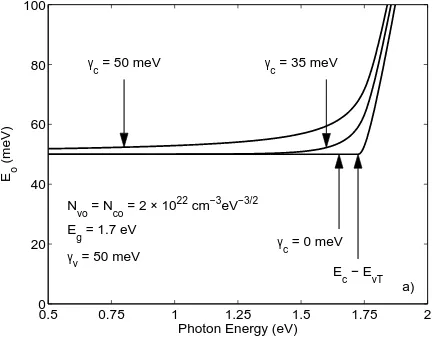
an evaluation of Eq. (2.2), for various selections of γc. For all cases, Nvo, Nco, Ev, Ec, and γv are held at their nominal a-Si:H values, i.e., Nvo = Nco = 2 ×1022 cm−3eV−3/2, Eg ≡ Ec− Ev = 1.7 eV, and γv = 50 meV. . . 69 2.3 The dependence of Eo, as defined in Eq. (2.8), on the photon energy,
~ω, for a number of selections of γc. For all cases, Nvo, Nco, Ev, Ec, and γv are held at their nominal a-Si:H values, i.e., Nvo = Nco = 2×1022 cm−3eV−3/2, Eg ≡Ec−Ev = 1.7 eV, andγv = 50 meV. . . . 71 2.4 The dependence ofEo, as defined in Eq. (2.8), on the conduction band
tail breadth, γc, for the photon energy, ~ω, set to 1 eV. For all cases, Nvo, Nco, Ev, Ec, and γv are held at their nominal a-Si:H values, i.e., Nvo =Nco = 2×1022 cm−3eV−3/2, Eg ≡Ec−Ev = 1.7 eV, and γv = 50 meV. The approximate analytical expression forEo, i.e., Eq. (2.9), is also depicted with the dotted line. . . 73 2.5 The dependence ofγv onγc. Results from the experiments of Sherman
et al. [29], Tiedje et al. [30], and Winer and Ley [31], are depicted. Results obtained from the modeling analysis of O’Leary [13] are also shown. . . 74
3.1 The valence band DOS function,Nv(E), for a number of selections of γv. This function, specified in Eq. (3.3) with EvT set to Ev −
1 2γv, is
evaluated assuming the nominal modeling parameter selections Nvo = 2×1022cm−3eV−3/2 andEv = 0 eV for all cases. The abscissa axis rep-resents the energy,E, while the ordinate axis depicts the corresponding valence band DOS value. . . 84 3.2 The dimensionless JDOS function, J (z), plotted as a function of z. . 87 3.3 The sensitivity of the JDOS function,J(~ω), to variations in the
crit-ical energy at which the exponential and square-root valence band distributions interface, EvT. All other modeling parameters are set to
points. Our calculated result is indicated with the solid line. The characteristic energy,Ed, is indicated with the arrow. We assume that Nvo = Nco = 2.38×1022 cm−3eV−3/2, Eg = 1.68 eV, γv = 48 meV, R2o = 10 ˚A2, andEd= 3.4 eV for the purposes of this analysis. We see that there is almost complete agreement between our model and the experimental results of Jacksonet al. [2], except for ~ω <1.4 eV. . . 90 3.5 Three a-Si:H optical absorption data sets plotted as a function of the
photon energy. The data sets considered include that corresponding to Cody et al. [18] (the TH = 293 K data set depicted in Figure 1
of Cody et al. [18]), plotted with the solid green points, Reme˘s [19] (the standard GD-a data set depicted in Figure 5.2 of Reme˘s [19]), plotted with the solid red points, and Viturro and Weiser [20] (the CH = 1 % data set depicted in Figure 4 of Viturro and Weiser [20]),
plotted with the blue solid points. The optical absorption spectral dependencies obtained through our theoretical analysis, for the cases ofγv = 68.9 meV andEg = 1.73 eV,γv = 91.2 meV andEg = 1.57 eV, and γv = 193 meV and Eg = 1.53 eV, are depicted using the green, red, and blue solid lines, respectively, these parameter selections being made in order to fit the theoretical results with the experimental data of Codyet al.[18], Reme˘s [19], and Viturro and Weiser [20], respectively; for all cases, we set Nvo = Nco = 2.38×1022 cm−3eV−3/2. The online version is depicted in color. . . 93 3.6 The rescaled a-Si:H optical absorption data sets and the
dimension-less JDOS function, J (z), plotted as a function of the independent variable, z. The data sets considered include that corresponding to Cody et al. [18] (the TH = 293 K data set depicted in Figure 1 of
Cody et al. [18]), plotted with the solid green points, Reme˘s [19] (the standard GD-a data set depicted in Figure 5.2 of Reme˘s [19]), plotted with the solid red points, and Viturro and Weiser [20] (the CH = 1 %
with the solid and open colored points. The solid colored points cor-respond to experimental data that is not believed to be influenced by defect absorption while the open colored points correspond to experi-mental data that is believed to be influenced by defect absorption. The color scheme is indicated in the legend within the figure. The identifi-cation of each data set borrows directly from the classifiidentifi-cation scheme employed by Codyet al. [17]; see Figure 1 of Codyet al.[17]. The fits to these experimental data sets are depicted with the corresponding colored lines. The model parameter selections for these fits, i.e., the correspondingγv and Eg values, are indicated in Table 4.1. The online version of this figure is depicted in color. . . 105 4.2 The rescaled experimental a-Si:H optical absorption data sets of Cody
et al. [17] and the dimensionless JDOS function, J (z), plotted as a function of the independent variable, z. The rescaled experimental data is represented with the solid and open colored points. The solid colored points correspond to rescaled experimental data that is not believed to be influenced by defect absorption while the open colored points correspond to rescaled experimental data that is believed to be influenced by defect absorption. The color scheme is indicated in the legend within the figure. The identification of each data set borrows directly from the classification scheme employed by Cody et al. [17]; see Figure 1 of Cody et al. [17]. The dimensionless JDOS function, J (z), plotted as a function of z, is also shown with the solid black line. The online version of this figure is depicted in color. . . 108 4.3 The experimental a-Si:H optical absorption data sets of Viturro and
plotted as a function of the independent variable, z. The rescaled ex-perimental data itself is represented with the solid points; for the case of Viturro and Weiser [27] there are no experimental points that are believed to be contaminated with defect absorption. The color scheme is indicated in the legend within the figure. The identification of each data set borrows directly from the classification scheme employed by Viturro and Weiser [27]; see Figure 4 of Viturro and Weiser [27]. The dimensionless JDOS function,J (z), plotted as a function of z, is also shown with the solid black line. The online version of this figure is depicted in color. . . 112 4.5 The experimental a-Si:H optical absorption data sets of Reme˘s [28] and
the corresponding fits. The experimental data itself is represented with the solid points; for the case of Reme˘s [28] there are no experimental points that are believed to be contaminated with defect absorption. The HW70 a-Si:H film of Reme˘s [28] is not considered as it exhibits a spectral variation that is distinct from the other spectra for high values of ~ω; it is depicted with the open points. The color scheme is indicated in the legend within the figure. The identification of each data set borrows directly from the classification scheme employed by Reme˘s [28]; see Figure 5.2 of Reme˘s [28]. The fits to these experimental data sets are depicted with the corresponding colored lines. The model parameter selections for these fits, i.e., the corresponding γv and Eg values, are indicated in Table 4.3. The online version of this figure is depicted in color. . . 114 4.6 The rescaled experimental a-Si:H optical absorption data sets of Reme˘s [28]
for the experimental a-Si:H optical absorption data sets of Cody et al. [17]. The ordinate values for this plot are obtained by dividing each experimental value,αexpt, by the corresponding fit value, αfit, the
abscissa axis being the corresponding photon energy, ~ω. The online version of this figure is depicted in color. . . 117 4.8 Deviations between the experimental results and the corresponding fits
as determined through a ratio of the experimental and fit results for the experimental a-Si:H optical absorption data sets of Viturro and Weiser [27]. The ordinate values for this plot are obtained by dividing each experimental value,αexpt, by the corresponding fit value, αfit, the
abscissa axis being the corresponding photon energy, ~ω. The online version of this figure is depicted in color. . . 119 4.9 Deviations between the experimental results and the corresponding fits
as determined through a ratio of the experimental and fit results for the experimental a-Si:H optical absorption data sets of Reme˘s [28]. The ordinate values for this plot are obtained by dividing each experimental value, αexpt, by the corresponding fit value,αfit, the abscissa axis being
the corresponding photon energy,~ω. The online version of this figure is depicted in color. . . 120 4.10 Deviations between the experimental results and the corresponding fits
as determined through a ratio of the experimental and fit results for the experimental a-Si:H optical absorption data sets of Codyet al.[17], Viturro and Weiser [27], and Reme˘s [28]. The ordinate values for this plot are obtained by dividing each experimental value, αexpt, by the
corresponding fit value,αfit, the abscissa axis being the corresponding
photon energy, ~ω. For the optical absorption values not influenced by defect absorption, 219 of the 290 experimental points of Cody et al.[17], 117 of the 176 experimental points of Viturro and Weiser [27], and 136 of the 181 experimental points of Reme˘s [28], lie between β1αfit
and βαfit, for the specific case of β set to 1.1. . . 121
4.11 The fraction of the experimental points between 1βαfit and βαfit as a
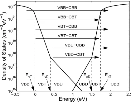
is determined assuming the nominal a-Si:H parameter selectionsNvo = 2×1022 cm−3eV−3/2, E
v = 0.0 eV, γv = 50 meV, Ev−EvT = 35 meV, γvD = 130 meV, and EvD −Ev = 400 meV. The conduction band
DOS function, Nc(E), specified in Eq. (5.6), is determined assum-ing the nominal parameter selections Nco = 2 × 1022 cm−3eV−3/2, Ec = 1.7 eV, γc = 27 meV, EcT−Ec = 35 meV, γcD = 80 meV, and Ec−EcD = 200 meV. The critical points at which the band states and
tail states interface,EvT and EcT, are clearly marked with the dashed
lines and the arrows. The critical points at which the tail states and defect states interface,EvD and EcD, are also marked with the dashed
lines and the arrows. Representative VBB-CBB, VBB-CBT, VBT-CBB, VBT-CBT, VBD-VBT-CBB, and VBD-CBT optical transitions are depicted. Representative VBB-CBD, VBT-CBD, and VBD-CBD op-tical transitions are not depicted as they are found to make relatively minor contributions to the JDOS function. . . 135 5.2 The JDOS function,J(~ω), associated with a-Si:H, determined through
an evaluation of Eq. (5.2). For the purposes of this analysis, we per-formed this evaluation with and without the defect states taken into account. In the absence of defects,Nv(E) andNc(E) are as specified in Eqs. (5.3) and (5.4), respectively. With defects taken into account, Nv(E) andNc(E) are as specified in Eqs. (5.5) and (5.6), respectively. The modeling parameters are set to their nominal a-Si:H values for the purposes of this analysis; recall Table 5.1. EcT−EvT and EcT−EvD,
attributable to the VBB-CBB optical transitions is shown with the solid blue line. The contribution attributable to the VBB-CBT opti-cal transitions is shown with the solid red line. The contribution at-tributable to the VBT-CBB optical transitions is shown with the solid green line. The contribution attributable to the VBT-CBT optical transitions is shown with the solid yellow line. The contribution at-tributable to the VBD-CBB optical transitions is shown with the solid purple line. The contribution attributable to the VBD-CBT optical transitions is shown with the solid light blue line. The contributions to the JDOS function attributable to the VBB-CBD, VBT-CBD, and VBD-CBD optical transitions are not depicted as they are found to make relatively minor contributions to the JDOS function. The mod-eling parameters are set to their nominal a-Si:H values for the purposes of this analysis; recall Table 5.1. EcT −EvT and EcT −EvD, critical
energies in our JDOS analysis, are clearly marked with the dashed lines and the arrows. The online version is in color. . . 138 5.4 The optical absorption spectrum, α(~ω), associated with a-Si:H. The
experimental data of Reme˘s [33] is depicted with the solid points; this experimental data set corresponds to the “standard GD-a” data set de-picted in Figure 5.2 of Reme˘s [33]. The fit to this data set, determined using the modeling parameter selections specified in Table 5.2, is shown with the solid line. The fit of the lower portion of this spectrum to an exponential function,αoDexp
~ω EoD
, is shown with the dashed line; the fit was obtained for experimental data with ~ω <1.4 eV. The dashed line corresponding to this fit has been extrapolated out to 1.45 eV so that it is observable. The determined value of EoD corresponding to
a-C amorphous carbon
a-Ge amorphous germanium
γc breadth of the conduction band tail
γv breadth of the valence band tail
c-Si crystalline silicon
CBB conduction band band
CBT conduction band tail
Ec conduction band band edge
EcT conduction band critical energy
Nc(E) conduction band density of states function
Nco conduction band DOS prefactor
DOS density of states
HW hot-wire
a-Si:H hydrogenated amorphous silicon
2(~ω) imaginary part of the dielectric function
J(~ω) joint density of states function
JDOS joint density of states
Si silicon
n, n(~ω) the refractive index
Ev valence band band edge
EvT valence band critical energy
Nv(E) valence band density of states function
Nvo valence band DOS prefactor
VBB valence band band
Introduction
1.1
Introduction to disordered semiconductors
Much of the progress that has occurred in electronics over the years has arisen as
a result of making the constituent electron devices within electronic systems faster,
smaller, cheaper, and more reliable. These developments have occurred as a
conse-quence of a detailed and quantitative understanding of the material properties of the
materials used in the fabrication of these devices. Electron devices are fabricated
from conductors, insulators, and semiconductors. While conductors and insulators
have been well understood for many years, interest in the material properties of
semi-conductors really only found its genesis with the fabrication of the first transistor in
1947 [1, 2]; prior to that time, semiconductors were considered a laboratory
curios-ity. Since that time, however, there has been a considerable amount of study into
the material properties of these materials. As further progress in electronics will
un-doubtedly require an even greater understanding of the properties of these materials,
it seems likely that interest in the material properties of semiconductors will remain
intense for many years to come.
are electron devices that require larger sizes in order to be useful. Displays [3, 4],
scanners [5], solar cells [6, 7], and x-ray image detectors [8], for example, are all large
area electron devices. The focus in large area electronics, as this field is now referred
to as, is on substrates of the order of a square-meter [9]. This contrasts with the
sub-micron device feature focus of conventional electronics. As crystalline silicon
(c-Si), the material which dominates conventional electronics, can not be deposited over
large areas, alternate electronic materials must be employed instead for large area
electron device applications [10, 11]. Typically, the electronic materials employed
for large area electronics are deposited as thin films over a substrate. Examples
of such materials include hydrogenated amorphous silicon (a-Si:H), polycrystalline
silicon (poly-Si), amorphous selenium (a-Se), and amorphous carbon (a-C). These
materials are collectively referred to as disordered semiconductors, as the distribution
of their constituent atoms does not possess the long-range order characteristic of a
crystalline semiconductor.
Progress in large area electronics has occurred through advances in our
under-standing of the material properties of disordered semiconductors. The study of such
semiconductors was initiated in the 1950s. Initially, chalcogenide semiconducting
glasses [12–14], such as As2Se3 and GeS2, were the focus of attention; chalcogenide
glasses refer to those that include the elements sulfur (S), selenium (Se), and tellurium
(Te), the chalcogen elements referring to those in column VI of the periodic table.
Pioneering studies into the material properties of these glasses, which are fabricated
by cooling from a melt [11], allowed researchers to first probe the important role that
disorder plays in shaping the electronic properties of these materials [12, 13, 15, 16].
In addition, a number of interesting device applications were implemented as a result
of these studies. For example, the first xerographic copying machine was fabricated
Interest in amorphous silicon (a-Si) began in the 1960s. Initially, a-Si was
pre-pared through sputtering or thermal evaporation [11]. Unfortunately, the material
that was produced was of extremely poor quality. Defects, arising as a consequence of
dangling bonds and vacancies, led to distributions of electronic states deep within the
gap region. This rendered the material extremely difficult to dope. In addition, the
disorder present made the resultant electron and hole transport very poor. In
partic-ular, the mobilities found in a-Si are orders of magnitude lower than those found for
c-Si. As a result, initially at least, a-Si did not attract much attention.
Hydrogenated amorphous silicon (a-Si:H) was a late arrival in the study of
disor-dered semiconductors [11]. It was found to exhibit much improved electronic
proper-ties when contrasted with that of its unhydrogenated counterpart. As a consequence,
it is considered much more appropriate for electron device applications. This
ma-terial was first fabricated in the late 1960s [11] through the use of glow discharge
deposition [17]. Since that time, a variety of deposition techniques, such as
hot-wire (HW), chemical vapour deposition (CVD), plasma enhanced chemical vapour
deposition (PECVD), and others, have been employed in order to produce this
mate-rial [18]. The improved electronic properties of a-Si:H were found to arise primarily as
a consequence of the passivation of the dangling bonds with hydrogen atoms. These
passivated dangling bonds do not contribute to the electronic states within the gap.
As a consequence, the number of electronic states within the gap is greatly reduced for
a-Si:H. This makes the material much more suitable for electron device applications.
There are a number of features associated with a-Si:H that make it a useful
ma-terial for electron device applications. In particular, it can be doped [19], it exhibits
a reasonable photoconductive response [11], and junctions may be readily formed [20]
using a-Si:H. Using modern plasma deposition techniques, a-Si:H may be
silicon based, many of the device processing techniques that have been developed for
the case of c-Si can also be employed for the case of a-Si:H. Finally, the same plasma
deposition technique that is used to fabricate the material itself may also be used
to deposit the dielectric and passivation layers needed for the realization of actual
devices [22].
1.2
Distribution of atoms
Crystalline silicon (c-Si) is a tetrahedrally bonded material. That is, each silicon
atom within c-Si is bonded to four other nearest neighbor silicon atoms. Ideally,
the bonding environment about each such atom is exactly the same as all of the
other silicon atoms within the crystal. This tetrahedral structure is thus repeated
periodically throughout the entire volume of the crystal. As a consequence, ideal c-Si
is said to possess long-range order. A two-dimensional schematic representation of
the long-range order characteristic of c-Si is shown in Figure 1.1 [23]. A defect within
c-Si corresponds to any departure from this perfect order.
In amorphous silicon (a-Si), however, such long-range order is not present. While
most silicon atoms within a-Si are bonded to four other silicon atoms, there are
vari-ations in the bonding environment from one silicon atom to the next. In particular,
variations in the bond lengths and bond angles occur. Dangling bonds are also found,
although it should be noted that dangling bonds are much rarer than their
tetrahe-dral counterparts; within a-Si, there are typically of the order of 1019 dangling bonds
per cm3 [11] while there are of the order of 1023 tetrahedral bonds per cm3, i.e.,
there is one dangling bond for every 10,000 tetrahedral bonds in a-Si. As a result
of these variations in the bond lengths and bond angles, a-Si is said to possess no
long-range order. Owing to the fact that the environment around any given silicon
crystalline
silicon
amorphous
silicon
form of short-range order. A two-dimensional representation of the short-range order
characteristic of a-Si is also depicted in Figure 1.1 [23].
Ideal a-Si corresponds to a fully bonded tetrahedral network of silicon atoms,
i.e., each silicon atom is bonded to four other silicon atoms. While such a continuous
random network may be ideal for the case of a-Si, disorder is present, even within the
framework of this ideal theoretical construct, i.e., variations in the bond lengths and
bond angles occur, these being inherent to the amorphous state. Any departure from
such an ideal network corresponds to the presence of a defect within a-Si. Vacancies
and dangling bonds are examples of defects that are present within a-Si. These
defects may be characterized in terms of the coordination number associated with each
silicon atom, the coordination number being the number of nearest neighbor atoms
associated with the atom in question. In an ideal a-Si network, all atoms are fully
coordinated, i.e., the coordination number associated with each silicon atom is four.
In contrast, with defects being present, variations in the coordination number of the
constituent silicon atoms within a-Si are found. Such variations in the coordination
number, corresponding to the specific case of a-Si, are schematically represented in
Figure 1.2.
Within an a-Si network, the displacement of one silicon atom from its usual
posi-tion will create dangling bonds with its four neighboring silicon atoms, each
neighbor-ing silicon atom havneighbor-ing a danglneighbor-ing bond [18]. A schematic representation of silicon
dangling bonds within a-Si is shown in Figure 1.3. For the case of a-Si:H, however,
Si-Si bonds, Si-H bonds, and silicon dangling bonds are found. Detailed studies have
found that the hydrogen atoms within a-Si:H, which are present in copious
quanti-ties during the deposition process and in the resultant a-Si:H films, bond to most of
the dangling bonds that are present within a-Si; most device-quality a-Si:H films are
Co-ordination Numbers
4
3
2
1
bonds found within a-Si:H is thus substantially reduced when contrasted with that of
its unhydrogenated counterpart, a-Si; there are typically of the order of 1015 dangling bonds per cm3 within device quality a-Si:H [11]. Many of the hydrogen atoms that are present within a-Si:H are singly coordinated with their host silicon atoms.
1.3
Device applications
Disordered semiconductors are employed in a variety of device applications. Early
applications of disordered semiconductors include the aforementioned a-Se
photocon-ductor based xerographic copying machine that was introduced to the market in the
1950s and the a-Si:H based photovoltaic solar cell that was introduced to the market
in the 1970s. Specifically focusing on the case of a-Si:H, this being the most widely
used disordered semiconductor today, current major applications for this material
in-clude displays, solar cells, thin-film opto-electronic devices, photoreceptors, sensors,
light emitting diodes, x-ray imagers, and scanners [3–8]. New applications are being
devised on a yearly basis.
At present, the primary use of a-Si:H is for electronic displays. These displays
cur-rently have a large market value, i.e., billions of dollars. Electronic displays are used
in televisions, computers, automobiles, telecommunication systems, and biomedical
systems. Each application has its own special requirements and customized
optimiza-tions must be performed with these requirements in mind. The diversity of electronic
display offerings will continue to grow as new applications are developed. Variations,
in terms of size, speed, power requirements, color range, brightness, contrast, and
many other parameters, are being offered [24].
Solar cells is another area in which a-Si:H is finding use. Solar cells are
semiconductor-based electron devices that are capable of producing electricity from solar energy
cells may be connected together into an array. At present, a-Si:H based solar cells
have an efficiency that ranges between 10 to 12 % [6, 7]. The solar cell panels should
last for twenty or more years, with low maintenance and low environmental impact.
That is, they do not produce air pollution, operate quietly, and do not interfere with
the natural environment.
1.4
The optical response
The performance of many of the devices fabricated from disordered
semiconduc-tors depends critically on the optical properties of these materials. Light attenuates
in intensity as it propagates through a material. Specifically, for monochromatic light,
i.e., all photons having the same value of photon energy, the intensity of light
dimin-ishes exponentially as it passes through a material. For the case of light normally
incident on a material, as shown in Figure 1.4, in the absence of any reflection, for
light propagating from the left, the intensity of the light, as a function of the depth
from the surface of the material, z, may be expressed as
I(z) = Ioexp(−αz), (1.1)
whereIo denotes the intensity at the surface of the material, z = 0, andα represents
the optical absorption coefficient. This coefficient describes the rate at which this
exponential attenuation occurs. A quantitative determination of this optical
absorp-tion coefficient,α, for various values of photon energy, will allow for the quantitative
analysis of the optical response of these materials. This in turn will allow for the
quantitative prediction of the device performance of many disordered semiconductor
based devices. Optimization of proposed designs may thus be considered.
op-light
Material
I(z)
I
0z
Figure 1.4: The intensity of light as a function of the depth, z, from the surface of the
material,z= 0, for light normally incident on a material and propagating from the left, in
tical absorption coefficient, α, depends on the photon energy, ~ω, i.e., α(~ω). From
the spectral dependence of the optical absorption coefficient, insights into the
char-acter of these materials may be gleaned. In a disorderless crystalline semiconductor,
the optical absorption spectrum terminates abruptly at the energy gap. In an
amor-phous semiconductor, however, the optical absorption spectrum instead encroaches
into the otherwise empty gap region. In Figure 1.5, the optical absorption spectrum
associated with a hypothetical crystalline semiconductor is contrasted with that of its
amorphous counterpart. While the optical absorption spectrum terminates abruptly
at the energy gap for the case of the hypothetical crystalline semiconductor, for the
case of an amorphous semiconductor, three distinct regions are observed. The
low-absorption region, i.e., α < 100 cm−1, denoted Region A in Figure 1.5, exhibits a
broad exponential dependence that encroaches deeply into the otherwise empty gap
region. The mid-absorption region, i.e., 100 cm−1 < α < 104 cm−1, Region B in
Figure 1.5, exhibits a sharp exponential increase corresponding to increased photon
energies, its breadth being much narrower than that exhibited by Region A. This
region is often referred to as the Urbach tail region, its breadth being referred to as
the Urbach tail breadth. It plays an important role in the physics of amorphous
semi-conductors, and has been the focus of a considerable amount of analysis. Finally, the
high-absorption region, i.e., α > 104 cm−1, denoted Region C in Figure 1.5, exhibits
an algebraic functional dependence.
This thesis aims to develop models that will allow for the quantitative analysis
of the spectral dependence of the optical absorption coefficient, α(~ω), associated
with a-Si:H. These models will stem from empirical models for the distributions of
electronic states, these distribution of electronic states models being rooted in a-Si:H
phenomenology. The ultimate aim of this analysis is to provide a framework for the
1
1.2
1.4
1.6
1.8
2
2.2
10
−110
010
110
210
310
4Energy (eV)
α
(cm
−1
)
crystalline semiconductor amorphous
semiconductor
A
B
C
Figure 1.5: The spectral dependence of the optical absorption coefficient, α(~ω),
the identification of general trends in these spectra. From the insights gleaned from
this study, greater understanding into the material properties of this semiconductor
will be obtained. These insights could be used in order to improve the performance
of future generations of a-Si:H based devices.
1.5
Distributions of electronic states
The disorder present within a-Si and a-Si:H has a profound impact on the
dis-tributions of electronic states. Accordingly, the electronic properties associated with
these materials are somewhat distinct from those exhibited by c-Si [11]. In a
dis-orderless material, these distributions terminate abruptly at the valence band and
conduction band band edges. This leads to a well defined energy gap that separates
the distribution of electronic states associated with the valence band from that
as-sociated with the conduction band. In contrast, in a-Si and a-Si:H, distributions of
electronic states encroach into the otherwise empty gap region. These tail states, as
the encroaching distributions of electronic states are often referred to as, are
associ-ated with the intrinsic disorder associassoci-ated with a-Si and a-Si:H, i.e., the unavoidable
variations in the bond lengths and bond angles. Defects, i.e., dangling bonds and
vacancies, are responsible for states deeper in the gap region. A schematic
represen-tation of these distributions of electronic states is depicted in Figure 1.6.
Detailed analyzes have demonstrated that some of the electronic states associated
with the tail states are actually localized by the disorder. That is, the wavefunctions
associated with such states are confined to a small volume rather than extending
throughout the entire volume of the material; all the wavefunctions associated with
ideal (disorderless) crystalline semiconductors extend throughout the entire volume
of the material. A comparison of the wavefunctions associated with localized and
demon-Energy
Distribution of Electronic States
defect states
valence band tail states
conduction band tail states valence band
band states
conduction band band states
extended electronic states
localized electronic states
strated that there exist critical energies, termed mobility edges, which separate the
localized electronic states from their extended counterparts, one associated with the
valence band, the other associated with the conduction band. That is, there is a
mo-bility edge associated with the valence band that separates the localized valence band
electronic states from their extended counterparts. Similarly, there is a mobility edge
associated with the conduction band that separates the localized conduction band
electronic states from their extended counterparts. These mobility edges are depicted
in Figure 1.8. The difference in energy between these mobility edges is referred to as
the mobility gap.
In the study of crystalline semiconductors, the periodicity inherent to the
dis-tribution of atoms allows for the quantitative determination of the energy levels of
the electronic states in terms of the electron wave-vector, ~k. The distributions of
electronic states that result may thus be characterized in terms of a band diagram
that specifies how the electronic energy levels vary with ~k. In the case of a
disor-dered semiconductor, however, such as a-Si and a-Si:H, the disorder renders~k a poor
quantum number. As a result, band diagrams can not be used for the analysis of
these materials. Nevertheless, as it is the nearest neighbor environment that
primar-ily determines the electronic character of a material, it seems reasonable to expect
the existence of bands within a-Si and a-Si:H, of similar shape and character to those
found within c-Si. As a consequence, it is expected that many of the properties found
for a-Si and a-Si:H are similar to those exhibited by c-Si.
In order to provide a quantitative framework for the determination of the
prop-erties associated with disordered semiconductors, an alternate approach to the band
diagrams used for the analysis of crystalline semiconductors must be sought. It is
found that the distributions of electronic states associated with these materials may be
Energy
Distribution of Electronic States
mobility gap
valence band conduction band
valence band mobility edge
conduction band mobility edge
states (DOS) functions, Nv(E) and Nc(E), respectively, Nv(E) ∆E and Nc(E) ∆E
representing the number of valence band and conduction band electronic states, per
unit volume, between energies [E, E+ ∆E]. This means of characterizing the
cor-responding distributions of electronic states may be employed both for crystalline
semiconductors and their amorphous counterparts.
1.6
Relation between the optical absorption
spec-trum and the DOS functions
For the specific case of a-Si:H, Jacksonet al.[26] developed a relationship between
the spectral dependence of the imaginary part of the dielectric function, 2(~ω), and
the valence band and conduction band DOS functions, Nv(E) and Nc(E),
respec-tively. This relationship is key to the analysis presented in this thesis. Accordingly, a
review of the analysis of Jackson et al. [26], relating 2(~ω) withNv(E) andNc(E), is presented in this section. The application of this relationship to the interpretation
of the optical properties associated with a-Si:H will be presented later in the thesis.
Jackson et al. [26] employ a linear response approach within the framework of
a one-electron formalism, i.e., many electron effects are neglected. Assuming
zero-temperature statistics, i.e., that all valence band states are completely filled and that
all conduction band states are completely empty, Jackson et al. [26] contend that
2(~ω) = (2πq)2
2 V
X
v,c
|~η·R~v,c|2δ(Ec−Ev−~ω), (1.2)
where q is the electron charge, V is the illuminated volume, ~η is the polarization
vector, andR~v,c=< c|~r|v > is the dipole matrix element associated with the valence
band and conduction band electronic states, |v> and |c>, respectively, the sum in
band; as this expression for2(~ω) is expressed in terms of the dipole matrix elements,
the general approach adopted by Jacksonet al. [26] is referred to as a dipole operator
based formalism. For unpolarized light, on average,|~η·R~v,c|2 reduces to
|Rv,c|2
3 , where
|Rv,c| denotes the amplitude of the dipole matrix element. Accordingly, Eq. (1.2)
reduces to
2(~ω) = (2πq)2
2 3V
X
v,c
|Rv,c|2δ(Ec−Ev−~ω). (1.3) Defining the average squared dipole matrix element
[R0(~ω)]2 ≡ P
v,c|Rv,c|2δ(Ec−Ev−~ω) P
v,cδ(Ec−Ev −~ω)
, (1.4)
Jackson et al. [26] conclude that
2(~ω) = (2πq)2
2 3V [R
0
(~ω)]2X v,c
δ(Ec−Ev −~ω). (1.5)
Thus far, the expression for 2(~ω) that has been derived, i.e., Eq. (1.5), applies
equally to both c-Si and a-Si:H. In order to facilitate a direct comparison between
the spectral dependencies of [R0(~ω)]2 associated with these two distinct materials, it would seem reasonable that this matrix element should be normalized by the number
of optical transitions corresponding to each material. The number of optical
tran-sitions from any given single-spin state in the valence band, associated with a-Si:H
and c-Si, are shown in Figure 1.9. In a-Si:H, the number of optical transitions from
any given single-spin state in the valence band is 2ρAV, ρA denoting the density of
silicon atoms within a-Si:H. In contrast, for the case of c-Si, the number of optical
transitions from any given single-spin state in the valence band is four; all of these
Energy
k
E
F4
a-Si:H c-Si
2
ρ
AV
Figure 1.9: The number of optical transitions allowed from a single-spin state in the valence band for the cases of c-Si and a-Si:H. For the case of a-Si:H, there are 2ρAV possible
occur from any given single-spin state in the valence band associated with a-Si:H is
greater than that associated with c-Si, and thus, it might be expected that the dipole
matrix elements associated with these transitions are of a lesser magnitude than those
associated with c-Si. Thus, a normalized average squared dipole matrix element,
R2(
~ω)≡[R0(~ω)]2
2ρAV 4
, (1.6)
is introduced, this matrix element being normalized by the ratio of the number of
optical transitions allowed for the case of a-Si:H with respect to that allowed for the
case of c-Si. Accordingly, Eq. (1.5) reduces to
2(~ω) = (2πq) 2 1
3ρAR
2(
~ω) 4 V2
X
v,c
δ(Ec−Ev−~ω). (1.7)
From the definition of a single-spin state, it may be seen that
Nv(E) = 2 V
X
v
δ(E−Ev), (1.8)
and
Nc(E) = 2 V
X
c
δ(E−Ec). (1.9)
By introducing the joint density of states (JDOS) function
J(~ω)≡ Z ∞
−∞
Nv(E)Nc(E+~ω), (1.10)
from Eqs. (1.8) and (1.9), it can be shown that
J(~ω) = 4 V2
X
v,c
Thus, using Eq. (1.11), Eq. (1.7) may be represented as
2(~ω) = (2πq)2
1 3ρAR
2(
~ω)J(~ω). (1.12)
For the specific case of a-Si:H, where ρAis roughly 5×10²²per cm−3, Eq. (1.12) may be simply expressed as
2(~ω) = 4.3×10−45R2(~ω)J(~ω), (1.13)
whereR2(~ω) is in units of ˚A2 and J(~ω) is in units of states2eV−1cm−6. It is upon this expression that the subsequent analysis is built.
The spectral dependence of the optical absorption coefficient, α(~ω), may be
determined by noting that
α(~ω) = ω
n(~ω)c2(~ω), (1.14)
wheren(~ω) denotes the spectral dependence of the refractive index and crepresents
the speed of light in a vacuum. For the purposes of this analysis, the spectral
depen-dence ofn(~ω) is determined by fitting a tenth-order polynomial to the experimental
data of Klazes et al. [27]; the original experimental data is depicted in Figure 4 of
Klazes et al.[27]. The resultant fit, and the original experimental data, are depicted
in Figure 1.10. This fit is only valid over the range of the experimental data of Klazes
et al. [27], i.e., for 0.77 eV <~ω <3.2 eV.
1.7
Free electron density of states
In light of the important role that the form of the valence band and conduction
0.5
1
1.5
2
2.5
3
3.5
3.4
3.6
3.8
4
4.2
4.4
4.6
4.8
5
Energy (eV)
n
experimental data
resultant fit
of the optical absorption spectra, it is obvious that they must be determined in order
for this analysis to proceed. It is instructive to consider the form of the density of
states for the free electron case. Consider an electron confined within a cubic volume,
of dimensions L×L×L, surrounded by infinite potential barriers; see Figure 1.11.
According to quantum mechanics, in steady-state, the wavefunctions associated with
this electron may be described by Schr¨odinger’s equation, i.e.,
− ~
2
2m∇
2
Ψ (~r) +V (~r) Ψ (~r) =EΨ (~r), (1.15)
where~denotes the reduced Planck’s constant,mrepresents the mass of the electron,
V (~r) is the potential energy, and E is the electron energy; in three-dimensions, ∇2
represents the mathematical operator ∂x∂22 +
∂2
∂y2 +
∂2
∂z2. If the electron is free within
the cubic volume, i.e., V (~r) = 0 for 0 ≤ x ≤ L, 0 ≤ y ≤ L, and 0 ≤ z ≤ L, and if
the potential is infinite elsewhere, then it may be shown that
Ψ (~r) = Ψnx,ny,nz(x, y, z) =
2 L
3/2
sinπnx L x
sinπny L y
sinπnz L z
, (1.16)
where nx, ny, andnz denote the quantum numbers, i.e., positive integers, associated
with electron motion in the x, y, and z directions, respectively. It should be noted
that on account of the electron spin, there are actually two electronic states associated
with each unique selection of nx, ny, and nz.
Substituting the solution for the wavefunction, i.e., Eq. (1.16), back into Schr¨odinger’s
equation, it is seen that
Enx,ny,nz = ~2 2m πnx L 2 + πny L 2 + πnz L 2 , (1.17)
y
x
L
L
L
z
V(x,y,z) = 0 - inside box
V(x,y,z) =
∞
- outside box
L
If one was to consider each unique combination of quantum numbers, nx, ny, andnz,
as a unique point in a contellation of such points in the first octet of three-dimensional
n-space, such as that shown in Figure 1.12, for sufficiently high energies, i.e., when the
granularity of these points becomes a continuum, it is seen that the radial quantum
number, i.e., the radius within which all selections of nx, ny, and nz, yield energies
less than or equal to E,
˜ n(E) =
r
2mL2E
~2π2 . (1.18)
Thus, the number of electronic states, per unit volume, up to and including energy
E, may be expressed as an integral over the DOS function, i.e.,
Z E
−∞
N(u) du= 2
4π 3
1 8
1
L3 n˜(E) 3
, (1.19)
where the factor of two refers to the two spin levels per unique selection ofnx,ny, and
nz, the factor of 43π denotes the prefactor for a spherical volume, the factor of eight in the denominator corresponding to the fact the nx,ny, andnz integers only occupy
the first octet of three-dimensional n-space, and the factor of L3 represents the fact
that this is defined on a per unit volume basis; there is a unity density of points in
the first octet of three-dimensionaln-space. Differentiation of Eq. (1.19) yields
N(E) = √
2m3/2 π2
~3
√
E. (1.20)
It is seen that this DOS function has no dependence onL. That is, when the electron
becomes completely free, i.e., when L → ∞, the DOS function is exactly the same.
This square-root DOS function, also known as the free-electron DOS, will form the
0
1
2
3
4
0
1
2
3
4
0
1
2
3
4
n
zn
x
n
y
Figure 1.12: The quantum numbers, nx, ny, and nz, shown in the first octet of
1.8
A review of empirical density of states models
The exact form of the DOS functions associated with disordered semiconductors
remains the focus of considerable debate. There are fundamental questions related
to the nature of the band states and the tail states associated with each band. In
addition, the form of the defect states remains unknown. In fact, despite many
years of study, the exact role that disorder plays in shaping these DOS functions
remains unknown. Even for the case of a-Si:H, the most well studied disordered
semiconductor, the band tailing that occurs has been attributed both to disorder [28]
and to the presence of hydrogen atoms [29]. As a consequence, a specification for the
DOS functions, Nv(E) and Nc(E), that stems directly from first-principles, would
likely be too complex in order to allow for insights into the material properties of
these semiconductors to be gleaned.
For the purposes of materials characterization, and in order to predict device
per-formance, a number of empirical models for the valence band and conduction band
DOS functions, Nv(E) andNc(E), respectively, associated with disordered
semicon-ductors, have been devised. These models provide an elementary means whereby
the properties associated with disordered semiconductors may be determined. Most
empirical DOS models are built upon disordered semiconductor phenomenology. A
brief review of the empirical DOS models that have been developed for the analysis
of the optical properties of disordered semiconductors is provided next.
In 1966, Tauc et al. [30] introduced an empirical model for the valence band
and conduction band DOS functions. Tauc et al.[30] assumed the free electron DOS
That is, Tauc et al. [30] assumed that
Nv(E) =
0, E > Ev
Nvo p
Ev−E, E ≤Ev
, (1.21)
and
Nc(E) = Nco p
E−Ec, E ≥Ec
0, E < Ec
, (1.22)
where Nvo and Nco denote the valence band and conduction band DOS prefactors,
respectively, Ev and Ec representing the valence band and conduction band band
edges. This model for the DOS functions associated with a disordered semiconductor,
i.e., Eqs. (1.21) and (1.22), forms the basis for the most common interpretation for the
determination of the energy gap associated with such semiconductors. The resultant
DOS functions, for the nominal selection of DOS modeling parameters tabulated in
Table 1.1, are depicted in Figure 1.13. The use of this model in determining the
energy gap associated with a disordered semiconductor is further discussed in the
literature.
In 1981, Chenet al.[31] improved on the empirical DOS model of Taucet al.[30]
by grafting an exponential distribution of valence band tail states onto the
square-root distribution of valence band band states, the conduction band DOS function,
−0.5
1
0
0.5
1
1.5
2
2
3
4
5
6
7
8
9
10
x 10
21
N
c(
E
)
N
v(
E
)
Energy (eV)
DOS (cm
−3
eV
−1
)
Table 1.1: The nominal DOS modeling parameter selections employed for the empirical DOS models described in this section. These modeling parameters are representative of a-Si:H.
Parameter (units) Tauc et Chen et Redfield [32] Cody [33] O’Leary et al. [30] al. [31] al.[34]
Nvo (cm−3eV−3/2) 2×10²² 2×10²² - 2×10²² 2×10²² Nco (cm−3eV−3/2) 2×10²² 2×10²² - 2×10²² 2×10²² Nvo∗ (cm−3eV−3/2) - 5×10²¹ 5×10²¹ -
-Nco∗ (cm−3eV−3/2) - - 5×10²¹ -
-Ev (eV) 0.0 0.0 0.0 0.0 0.0
Ec (eV) 1.7 1.7 1.7 1.7 1.7
Ev−EvT (meV) - - - - 25
EcT −Ec (meV) - - - - 13.5
γv (meV) - 50 50 50 50
γc (meV) - - 27 - 27
Chen et al. [31] assumed that
Nv(E) =
Nvo∗ exp
Ev −E γv
, E > Ev
Nvo p
Ev −E, E ≤Ev
, (1.23)
and
Nc(E) = Nco p
E−Ec, E ≥Ec
0, E < Ec
, (1.24)
whereNvo∗ denotes the valence band tail DOS prefactor andγv represents the valence
band tail breadth, Nvo, Nco, Ev, and Ec being as defined earlier. The resultant
DOS functions, for the nominal selection of DOS modeling parameters tabulated in
Table 1.1, are depicted in Figure 1.14.
In an effort to understand how the valence band tail states and the conduction