ABSTRACT
HAN, Sungkee. Fabrication and Device Characterization of Alternative Gate Stacks Using the Non Self-Aligned Gate Process (Under the direction of Carlton M. Osburn)
In order to improve MOSFET transistor performance, aggressive scaling of devices has continued. As lateral device dimensions continue to scale down, gate oxide thicknesses must also be scaled down. According to the 2001 International Technology Roadmap for Semiconductor (ITRS) for sub-micron technology, an equivalent oxide thickness (EOT) less than 1.0 nm is required for high performance devices. However, at this thickness SiO2 has reached its scaling limit due to the high tunneling current, especially in low power devcies. The use of high K dielectrics may circumvent this impediment since physically thicker dielectrics can be used to reduce gate leakage while maintaining the same level of inversion charge. In this study, we used an alternative, non self-aligned gate process to fabricate both NMOS and PMOS devices with a variety of high K gate dielectric and metal gate electrode materials; finally their electrical properties were characterized.
Wet and dry etching process for alternative high K gate dielectrics (HfO2, ZrO2, La2O3, Y2O3) and metal gate electrodes (Pt, Ru, RuO2, Ta, TaN) were studied. Wet etching of Pt and TaN required periodic re-baking of the photoresist to re-establish adhesion to the substrate. Reactive ion etch (RIE) processes were developed for RuO2, Ru/W, Ta/W gate electrodes. A mixture of oxygen and fluorine plasma was effective in patterning RuO2 electrodes. However, for Ru gate electrodes, etch rates only up to 6.7 nm/min could be obtained even with the optimized addition of a few percent Cl2 to O2; this etch rate was considerably slower than that of photoresist. Rather than using a hard mask to etch the Ru gate, a laminated gate composed of a thin Ru layer (3 nm) covered with a thicker W film (100 nm) was successfully dry etched. The etching characteristics of various high K gate dielectrics depended not only on the materials, but also on how they were deposited, including the substrate pretreatment and post deposition anneal conditions. For instance, jet vapor deposited (JVD) HfO2 would etch in BOE (10% HF), while other HfO2 films required dry etching. Similarly, rapid thermal CVD (RTCVD) ZrO2 required dry etching while other ZrO2 films could be wet etched in BOE.
good C-V characteristics were observed for HfO2 (JVD) and ZrO2 (JVD and RTCVD) except for the devices having TaN gate electrodes. Due to over-etching, a large die-to-die variability was observed with TaN gated capacitors. The measured EOT values for HfO2 and ZrO2 films ranged from 1.28 to 2.25 nm and 1.86 to 2.62 nm, respectively. The RTCVD HfO2 and JVD ZrO2 had the same gate leakage as reported values, while slightly higher leakages were observed with JVD HfO2 and RTCVD ZrO2. Nevertheless, most of the devices having HfO2 or ZrO2 dielectrics met the low operating power gate leakage specifications (0.81 A/cm2 at 1.0 V) for the 100 nm and 70 nm ITRS technology nodes in our experimental splits. Devices made with physical vapor deposited (PVD) HfO2 had the thinnest EOT (0.9 nm with Ru/W gate and 1.2 nm with poly-silicon gate).
The effect of forming gas annealing, 10% H2 in 90 % N2, on PVD HfO2 was studied. We found that H2 annealing showed significant enhancements in drive current and channel mobility. But even with H2 annealing, HfO2 still had lower mobility than high quality SiO2. In order to further enhance its interface quality, D2 forming gas annealing, 10% H2 in 90 % N2, was performed. Even though the detailed mechanism has not been revealed, D2 annealing gave a greater increase in device current and mobility than H2.
degrade during the poly-silicon process. Experiments were designed with Hf silicate dielectrics to separately examine the thermal degradation during the high temperature poly-silicon activation cycle and chemical reaction during and after the poly-silicon CVD process. Al gated Hf silicate devices revealed no significant degradation even with pre-metal annealing temperatures up to 1000 ºC. Devices having different sources of poly-silicon gates (LPCVD poly-poly-silicon, LPCVD amorphous poly-silicon, and sputter deposit amorphous silicon) and metal gates were compared to examine the chemical reactions with the poly-silicon. Regardless of the depositions method, all devices with poly-silicon gates showed considerable degradation. Even though the high thermal budget itself had a negligible effect, the combination of high temperature annealing and the presence of silicon gates degraded Hf-based dielectrics.
FABRICATION AND DEVICE CHARACTERIZATION OF
ALTERNATIVE GATE STACKS USING THE NON SELF-ALIGNED
GATE PROCESS
by
SUNGKEE HAN
A dissertation submitted to the Graduate Faculty of North Carolina State University
in partial fulfillment of the requirements for the Degree of
Doctor of Philosophy
MATERIALS SCIENCE AND ENGINEERING
Raleigh, NC April 2003
APPROVED BY:
____________________________ ____________________________ Dr. Carlton M. Osburn Dr. Jon-Paul Maria
Co-chair of Advisory Committee Co-chair of Advisory Committee
____________________________ ____________________________
BIOGRAPHY
Sungkee Han was born on April 24, 1971 in Seoul Korea. When he was 18, his family moved to New York City. He attended John Bowne High School in Flushing, New York and graduated in 1991. In that same year, he entered Rensselaer Polytechnic Institute, Troy, New York. In 1995, he completed his bachelor of science in Materials Science and Engineering and began graduate school at North Carolina State University in Raleigh, North Carolina. In May 1998, he received his Master of Science degree in Materials Science and Engineering. In June of 1998, he enrolled in the Materials Science and Engineering Ph.D. program. During the course of his research under the direction of Dr. Carlton Osburn, he studied new device integration strategies for high K gate dielectric and new gate electrode materials that meet the 70 and 50 nm technology nodes at the SRC/SEMATECH Center for Front End Processes. In August 2003, he received his Doctor of Philosophy degree in Materials Science and Enginerring.
ACKNOWLEDGMENTS
I would like to express my sincere appreciation to my advisory committee members, Dr. Carlton Osburn, Dr. Jon-Paul Maria, Dr. Gerald Lucovsky and Dr. George Rozgonyi for providing guidance in the research and review of this thesis. I owe special thanks to my advisor, Dr. Carlton Osburn. Without his guidance and financial support this work would not have been possible. I also thank Dr. Jon-Paul Maria who serves as co-chairman of my advisory committee.
My sincere thanks are extended to members of the North Carolina State University Microelectronics Laboratory. In particular, my sincere thanks go to J. O’Sullivan, Harold Morton and Dr. D.Ginger Yu who provided invaluable assistance in the clean room.
I am grateful to current and former member of Dr.Osburn’s group, Kam Y. Lee, Indranil De and Indong Kim who have been excellent friends and colleagues throughout the years.
Sufficient thanks cannot be given to my parents, Moo Woo and Yon Ja Han, for their love and support. Special thank also goes to my one and only brother and his wife, Sung Dal Han and Yon Hee Han. Without their support, it would have been impossible to succeed in my study.
Last, but not least, I would like to thank to all of my friends, especially Se-Hwan Chung, Hoon Jae Yim, Ha Joon Hwang, Seung Wook Moon, Sung Joon Doh, Hyung Min Bae, Sung Won Ha, Dong Wook Jung, Joon Goo Hong, Jae Hoon Lee, You Seok
Suh, Ji Sang Hwang, Jin Ho Lee and Hyung Jik Lee, for their encouragement and support during my graduate study at NCSU.
TABLE OF CONTENTS
List of Tables………....vii
List of Figures……….viii
Chapter 1: Introduction 1.1. Scaling of Gate Oxide……….………1
1.2. Alternative High Dielectric Constant Gate Insulator Materials………..4
1.3. Metal Gate Candidates………...7
1.4. Outline of the Dissertation………...…9
1.5. Reference………...………11
Chapter 2: Device Fabrication Incorporating Alternative Gate Stack 2.1. Processing Issues Related to MOS Device Fabrication and Performance………….23
2.2. Replacement Gate Process……….24
2.3. Non-self Aligned Gate Process………..25
2.4. ERC 6 Mask Set……….26
2.5. Device Fabrication using the Non-self Aligned Gate Process………...28
2.6. Gate Dielectrics and Gate Metal Electrodes Deposition Methods……….30
2.7. Reference………33
Chapter 3: Etching of High K Gate Dielectrics and Gate Metal Candidates 3.1. Introduction……….…………...38
3.2. Experimental Procedure……….39
3.3. Results and Discussion………...41
3.3.1. Metal Gate Electrode Etching……….41
3.3.1.1. Platinum………...41
3.3.1.2. Tantalum Nitride………..42
3.3.1.3. Ruthenium Oxide……….43
3.3.1.4. Ruthenium, Tungsten, and Tantalum……… …..44
3.3.2. High K Dielectric Etching………..45
3.3.3. Device Characteristics………46
3.4. Summary and Conclusion………..47
3.5. Reference………...49
Chapter 4: Device Characterizations of Alternative Gate Stacks Using the Non-self Aligned Process 4.1. Introduction………59
4.2. Experimental Procedure……….59
4.3.1. Device Characteristics of Control Oxide……….62
4.3.2. Capacitance Voltage (C-V) and Gate Leakage (Ig-Vg) Characteristics of HfO2 and ZrO2……….62
4.4.3. Device Characteristics……….62
4.4.3. Effect of Forming Gas Anneal: H2 vs. D2………66
4.4. Conclusions……….67
4.5. Reference………69
Chapter 5: Gate Leakage Current Behavior of HfO2 and Hf Silicate with Poly-silicon and Metal Gate Electrode 5.1. Introduction………..…….104
5.2. Experimental……….105
5.3. Results……….………..107
5.3.1. Variability of Gate Leakage Current with Poly-silicon Gate……….107
5.3.2. Compatibility of Poly-silicon Gate on Hf Silicate……….109
5.4. Summary and Conclusion……….111
5.5. Reference………..113
Chapter 6: Gate Leakage Characteristics of Hf Silicate Alloys and Effect of Nitridation 6.1. Introduction………..……….129
6.2. Experimental……….131
6.3. Results……….…………..132
6.3.1. Gate Leakage of Hf Silicate Alloys………...132
6.3.2. Effect of Nitridation………...132
6.4. Conclusion………134
6.5. Reference………..136
Chapter 7: Summary and Conclusion 7.1. Non-self Aligned Gate Process and ERC 6 Mask Set………..151
7.2. Etching of High K Gate Dielectrics and Gate Metal Electrodes………..152
7.3. Device Characterization of Alternative Gate Stacks Using the Non-self Aligned Gate Process………153
7.4. Gate Leakage Current Behavior of HfO2 and Hf Silicate with Poly-silicon and Metal Gate Electrode………..154
7.5. Gate Leakage Characteristics of Hf Silicate and Effect of Nitridation……….155
7.6. Future Work………..155
Appendix A……….157
Appendix B……….164
Appendix C……….173
LIST OF TABLES
Table 1.1. Key properties of high K dielectric candidates………..6 Table 2.1. Summary of structures in ERC 6 mask set………...27 Table 2.2. Matrix of high K dielectrics and gate electrode materials………28
Table 2.3. High K dielectrics and metal gate electrodes deposition methods
and their deposition condition………..31
Table 3.1. Deposition methods and conditions for high K dielectric
and gate electrodes candidates………..40 Table 3.2. Etch rate, resistivity and their corresponding nitrogen content…………43 Table 3.3. Optimized etching recipes for metal gate electrode candidates…………45 Table 3.4. Etch process and etch rate for high K gate dielectrics candidates………46 Table 4.1. Deposition sources and their deposition methods for high K
Dielectric………...60 Table 4.2. Deposition sources and their deposition methods for gate
Electrodes………..61 Table 4.3. Equivalent oxide thickness of each dielectrics (the values
extracted from C-V measurements)………..63 Table 4.4. Summary of peak mobility and universal mobility scattering
parameters of before and after D2 and H2 forming gas annealing
(substrate doping = 3x10¹⁸/cm3)………...67 Table 5.1. HfO2 and Hf silicate deposition methods and their deposition
LIST OF FIGURES
Figure 1.1. Measured and simulated gate leakage currents for SiO2 dielectrics…..…21 Figure 1.2. Conduction and valance band calculations for high K gate
dielectric candidate materials……….…21 Figure 1.3. Energy level diagram of (a) midgap metal gates and (b) dual metal
Gate………22 Figure 1.4. Work function of metal gate candidates………22 Figure 2.1. Schematic illustration of replacement gate process: a) conventional
device fabrication using sacrificial gate oxide; b) oxide deposition and CMP planarization etch back; c) etch out sacrificial gate
stack; d) deposit new gate stack and pattern gate electrode……….……..35 Figure 2.2. Non-self aligned gate process chip layout (ERC6)………36
Figure 2.3. Schematic illustration of non-self aligned gate process: (a) grow and pattern 1000 Å thick oxide and form junction; (b) deposit LPCVD oxide over diffusions and pattern gate and contact regions; (c) deposit gate dielectric and electrode; (d) pattern and
etch gate electrode/dielectric and deposit and pattern contact metal…….37 Figure 3.1. AES analysis of: a) as deposited Pt film; (b) Pt film after standard
descum (300 Watts, 1 min of O2 Plasma); (c) Pt film after Ar+ ion
milling (80 Watts, 20 sccm at 60 mtorr for 3 minutes)……….…….52 Figure 3.2 XPS analysis of : a) TaN film on 4 inch wafer (low nitrogen
concentration); and b) TaN film on 6 inch wafer (high nitrogen
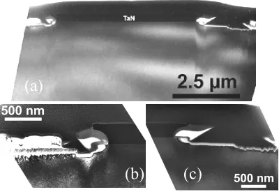
concentration………..53 Figure 3.3. The cross-section TEM view of the transistor with SiO2/TaN gate
stack: (a) overall view, (b) magnified TaN left edge view and
(c) magnified TaN right edge view………54 Figure 3.4. Etch rate of RuO2 film in O2/CHF3 plasma as a function of
CHF3/(O2+CHF3) ratio………...………55 Figure 3.5. Etch rate of Ru film in O2/Cl2 plasma as a function of Cl2/(O2+Cl2)
Figure 3.6. a) SEM micrograph Ru/W film etched in O2/Cl2 (20 sccm/1 sccm), at 40 mtorr, 150 Watts and b) SEM micrograph Ru/W film etched
in SF6/O2 (18 sccm/2 sccm), at 40 mtorr, 150 Watts……….56 Figure 3.7. a) NMOS subthreshold characteristics of MBE La2O3 with Ta/W
gate and b) PMOS ID-VG Characteristics of PVD HfO2 with Ru/W
gate……….57 Figure 3.8. a). Id-Vd characteristics of La2O3-TaN NMOS device and b) Id-Vd
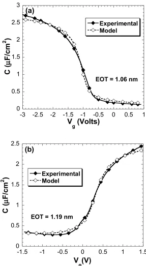
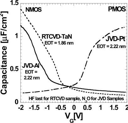
characteristics of HfO2 (JVD)-Pt PMOS device………58 Figure 4.1. High-frequency C-V characteristics of (a) NMOS capacitance and
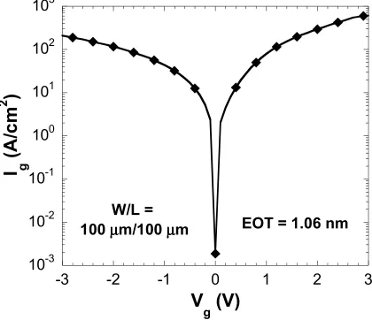
(b) PMOS capacitors……….…….72 Figure 4.2. NMOS Ig-Vg characteristic of control oxide (EOT = 1.06 nm) from
100 µm x 100 µm capacitor……….……..73
Figure 4.3. NMOS channel mobility of control oxide (Nif = 4.8 x10¹⁰/cm2, HxL
= 29.1 Å2)………..74
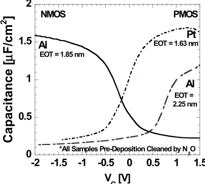
Figure 4.4. C-V characteristics of JVD HfO2. Al samples received 600˚C 20min FG post-deposition anneal, while Pt samples got 600˚C, 20min N2
annealing………75 Figure 4.5. C-V curves of ZrO2 with different metal gates. RTCVD samples
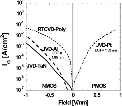
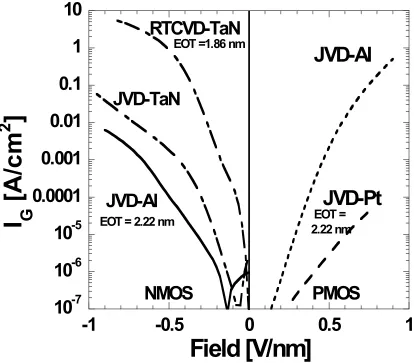
received, 900°C, 30sec N2 annealing while JVD samples got 550°C, 20min FG post-deposition annealing……….……76 Figure 4.6. Gate leakage characteristics of HfO2 with different gate electrodes…….77
Figure 4.7. Gate leakage characteristics of ZrO2 with different gate electrodes……..78
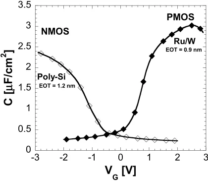
Figure 4.8. C-V characteristics of PVD HfO2 with poly-silicon (NMOS) and
Ru/W (PMOS) gate electrodes………..79 Figure 4.9. Gate leakage characteristics of PVD HfO2 with (a) poly-silicon
gates (NMOS) and (b) Ru/W (PMOS) gates……….………80 Figure 4.10. Subthreshold characteristics of (a) NMOS JVD and RTCVD HfO2
and (b) PMOS JVD HfO2 devices……….…………81 Figure 4.11. Subthreshold characteristics of (a) NMOS JVD and RTCVD ZrO2
Figure 4.12. Subthreshold characteristics of (a) NMOS PVD HfO2 with
poly-silicon and (b) PMOS PVD HfO2 with Ru/W gate electrodes….….83 Figure 4.13. Subthershold characteristics of La2O3 NMOS device with
TaN gate electrode……….…84 Figure 4.14. Id-Vd characteristics of JVD HfO2 with Al gated device………...85 Figure 4.15. Id-Vd characteristics of RTCVD HfO2 with poly-silicon gated
devices………...86 Figure 4.16. Id-Vd characteristics of JVD ZrO2 with TaN gated device……….87 Figure 4.17. Id-Vd characteristics of JVD ZrO2 Al gated NMOS device………88 Figure 4.18. Id-Vd characteristics of MBE La2O3 with TaN gated NMOS device…….89 Figure 4.19. Id-Vd characteristics of JVD HfO2 Pt gated PMOS device………90 Figure 4.20. Id-Vd characteristics of JVD ZrO2 with Pt gated PMOS device………….91 Figure 4.21. Extracted NMOS mobility (JVD and RTCVD HfO2, JVD and
RTCVD ZrO2, and MBE La2O3 devcies)………..………92 Figure 4.22. Extracted NMOS mobility of PVD HfO2 with poly-silicon gate…….….93 Figure 4.23. Extracted PMOS mobility (JVD HfO2 and JVD ZrO2)……….94 Figure 4.24. Extracted PMOS mobility of PVD HfO2 with poly-silicon gate….……..95 Figure 4.25. Gate leakage characteristics of HfO2 (1.2 nm) with poly-silicon
gates before and after H2 annealing……….………..96 Figure 4.26. C-V characteristics of HfO2 (1.2 nm) with poly-silicon gates
before and after H2 annealing………97 Figure 4.27. Id-Vg characteristics of HfO2 (1.2 nm) with poly-silicon gates
before and after H2 annealing………98 Figure 4.28. Mobility characteristics of HfO2 (1.2 nm) with poly-silicon gates
before and after H2 annealing………..………..99 Figure 4.29. Gate leakage characteristics of HfO2 (1.2 nm) with poly-silicon
gates before and after D2 annealing……….100
Figure 4.30. C-V characteristics of HfO2 (1.2 nm) with poly-silicon gates
before and after D2 annealing……….……….101 Figure 4.31. Id-Vg characteristics of HfO2 (1.2 nm) with poly-silicon gates
before and after D2 annealing. Id-Vg characteristics with H2
annealing are also shown to compare with D2 annealing………102 Figure 4.32. MOSFET mobility characteristics of HfO2 (1.2 nm) with
poly-silicon gates, before and after D2 annealing. Mobility characteristics with H2 annealing are also shown to compare
with D2 annealing……….103
Figure 5.1. Gate leakage characteristics of (a) PVD HfO2 with LPCVD poly-silicon gate electrode deposited at 550 ºC and (b) MOCVD
HfO2 with LPCVD poly-silicon gate electrode deposited at 650 ºC…...118 Figure 5.2. (a) PMOS gate leakage characteristics of PVD HfO2 with
Ru/W gate electrode and (b) NMOS gate leakage characteristics
of JVD HfO2 with Al gate electrode………..…..120 Figure 5.3. Gate leakage characteristics of MOCVD Hf silicate with
(a) LPCVD poly-silicon gate electrodes deposited at 650 ºC and
(b) Al metal gate electrodes……….…122 Figure 5.4. Histogram representations of gate leakage variability for both
poly-silicon and metal gate electrodes……….123 Figure 5.5. PVD HfO2 gate leakage characteristics of before and after breakdown..124
Figure 5.6. C-V Characteristics of Hf silicate capacitors with four different
temperatures (600 ºC, 800 ºC, 900 ºC, and 1000 ºC)………..….125 Figure 5.7. EOT variations with four different annealing temperature
(600 ºC, 800 ºC, 900 ºC, and 1000 ºC)………126 Figure 5.8. C-V characteristics of (a) three different silicon gates (LPCVD
poly-silicon, LPCVD amorphous silicon, and PVD amorphous
silicon) and (b) two different (Al and TaSixNy) metal gates………127 Figure 5.9. Gate leakage characteristics of (a) LPCVD amorphous-silicon,
(c) LPCVD poly-silicon, (c) PVD amorphous silicon, and
(d) metal gate electrodes………..128 Figure 6.1. Schematic illustration of (ZrO2)•(SiO2) phase separation after
xii
high temperature annealing under oxidizing conditions………..143
Figure 6.2. Gate leakage current (corrected for 1 nm EOT) at -1 V gate bias
for different silicate composition……….144 Figure 6.3. (a) C-V characteristics of Hf silicate/poly-silicon gate stack with
different nitridation conditions and (b) C-V characteristics of Hf
silicate/Al gate stack with different nitridation conditions………..145 Figure 6.4. (a) Interfacial and surface nitridation effect on EOT (Hf silicate
with Al gate) and (b) Interfacial and surface nitridation effect on
flat band voltages (Hf silicate with Al gate)………...147 Figure 6.5. (a) Interfacial and surface nitridation effect on EOT (Hf silicate
with poly-silicon gate) and (b) Interfacial and surface nitridation
CHAPTER 1
Introduction
1.1. Scaling of Gate Oxide
SiO2 has served as a nearly perfect gate dielectric for integrated circuit (IC) applications for more than 40 years. The primary reasons for this are that SiO2 (a) passivates the Si surface with a low surface-state density ~1-3 x 10¹⁰ (eV-cm2)-1; (b) serves as a patternable mask, forming a amorphous layer, for the localized diffusion of dopants into Si for p-n junction fabrication; (c) is an insulator with a large energy gap (~9 eV) and very few trap states. In order to meet the demands for improved transistor performance (e.g. improving circuit speed, reducing power and increasing packing density) the microelectronics revolution has continued, and IC density is quadrupling every three years [1-3]. Since the scaling of minimum feature sizes in MOSFETs has been the major driving for this revolution, gate oxide thickness must also be approximately linearly scaled down with channel length to maintain the same amount of gate control over the channel [4-6]. According to the 2002 International Technology Roadmap for Semiconductor (ITRS) [7] an equivalent oxide thickness (EOT) less than 1.0 nm is needed for a high performance microprocessor (MPU) for sub 100 nm Technology node. However, the scaling of conventional SiO2 gate dielectric into the sub 100 nm regimes aggravates serious problems.
spectroscopy (EELS), and they revealed that the full band gap of SiO2 was obtained for two monolayers of SiO2 [8]. Since the thickness of each SiO2 monolayer is about 3.5-4.0 Å, this will set a physical limit of SiO2 of 7-8 Å. Aside from its physical limitation, there is a practical limit for scaling down of the SiO2 thickness. Even though transistors with 13-15 Å thick gate oxide are still usable for high performance applications, they show high gate leakage current density (1-10 A/cm2) and may not be suitable for low power applications [9-10]. According to the Timp et al. SiO2 gate dielectrics thinner than 10-12 Å result in no improvement in transistor drive current [11-13]. Yu et al. also reported similar results [14].
High gate tunneling current is a major impediment to use the SiO2 as a gate dielectric in scaled MOSFETs. As the oxide thickness scales down below 1.5 nm, the direct tunneling gate-to-channel leakage current for SiO2 increases exponentially with decreasing oxide thickness [15-17]. Figure 1.1 shows experimental gate oxide tunneling currents for various oxide thicknesses from 3.5 nm to 1.4 nm, over a voltage range where direct tunneling dominates. When the gate leakage current becomes equal to the off-state source to drain sub-threshold leakage, the SiO2 thickness limit will be reached [16]. As shown in the Figure 1.1, the SiO2 gate dielectric thickness limit occurs at around 1.6 nm for devices with 100 nm gate length designed for 1.0V operation [15-17].
carrier quantization: (i) since the surface charges are located in localized energy levels above the edge of conduction band, additional band bending is required for the same amount of the inversion charge and (ii) the charge distribution is peaked further from the surface than classical theory would predict [22]. Due to the formation of a depletion layer near the polysilicon gate/oxide interface, a significant decrease in gate capacitance in inversion has been observed [21]. Lower polysilicon doping density, thinner gate oxide and high substrate doping results in an increase the polysilicon depletion effect. Both quantum mechanical quantization and polysilicon depletion effectively increase the separation of the gate and the inversion charge. This results in reduced gate control of channel inversion charge and can be interpreted as an increase in oxide thickness [23]. Dopant diffusion through the thin gate oxide, especially boron diffusion out of p+ polysilicon gate, is another problem in scaled MOSFETs. Boron penetration is enhanced when the gate oxide is scaled down [24]. In order to minimize gate dopant penetration through the gate oxide, the thermal cycle following the polysilicon implantation needs to be minimized.
1.0 nm), using an oxide/nitride stack is not beneficial since its high gate leakage and high interface trap density most likely will degrade device performance [31].
1.2. Alternative High Dielectric Constant Gate Insulator Materials
Higher dielectric constant (K) gate insulators may circumvent the problems facing conventional SiO2 gate insulators. With these alternative materials, physically thicker dielectrics can be used while maintaining the same level of inversion charge since the electric field is inversely related to the thickness of the dielectric layer. This reduces the probability of electrons and holes tunneling through the dielectric. Provided that band offsets are sufficiently large, the use of thicker dielectric layers results in less gate leakage current, thereby permitting further scaling of the dielectric thickness.
1.2.1. Materials Properties Requirements
In order to be used as a gate insulator, the alternative high K gate dielectric must meet a set of criteria, such as: appropriate barrier height, high dielectric constant, ability to form a stable interface with Si as well as the gate electrode at thermal stability, and has a good dielectric-silicon interface (low interface state densities, low fixed charge and smooth surface) to achieve high channel mobility.
dielectrics in series, the lowest capacitance layer will dominate the overall capacitance and set an oxide thickness-scaling limit. Furthermore, formation of a barrier layer increases the process complexity since it requires deposition or growth of an additional ultra thin dielectric. Due to this reason, it is desirable to have a high K dielectric that will be thermodynamically stable on Si.
It is essential that dielectric with a higher permittivity than SiO2 be used. But at the same time, the permittivity must be balanced with the band offset, which is the barrier height for tunneling process. Key properties (dielectric constants, band gaps and band offsets) of candidate materials are summarized in Table 1.1 and Figure 1.2 [32,33]. In order to have low gate leakage current, it is desirable to use a high K gate dielectric with large band offset. It is most likely that those oxide candidates with band offset less than 1.0 eV will not be used in gate dielectric applications.
1.2.2. High Dielectric Constant Gate Insulator Candidates Materials
Table 1.1. Key properties of high K dielectric candidates [32,33].
Materials Diele. Constant (K) Band Gap (eV) CB Offset (eV) VB Offset (eV)
SiO2 3.9 8.9 3.5 4.4
Si3N4 7 5.1 2.4 4.4
Al2O3 9 8.7 2.8 4.9
Y2O3 15 5.6 2.3 2.6
La2O3 30 4.3 2.3 2.6
TiO2 80 3.5
Ta2O5 26 4.5 0.3 3.0
ZrSiO4/ HfSiO4
13-26 1.5 3.4
HfO2 25 1.5 1.5 3.4
ZrO2 25 3.4 1.4 3.3
formation to temperatures as high as 900 ºC. C.H. Lee et al. showed ultra thin, high quality rapid thermal CVD deposition of ZrO2 on Si [48]. They showed for an EOT of 9 Å a low leakage current of 20 mA/cm2 at -1 V gate bias. Wilk et al. reported that an EOT less than 18 Å for a 50 Å Hf6Si29O65 film, which yields a dielectric constant ~11 [49]. Qi et al. studied sputtered silicate films (12% Zr); For an EOT of 14.5 Å; they reported a low leakage of 3.3x10⁻³ A/cm2 at –1.5 V [63].
In addition to HfO2 and ZrO2, La2O3 and Y2O3 have also been considered as alternative gate dielectric candidates due to their thermodynamic stability on Si and relatively high effective dielectric constant (~16-27) [66-70]. Chin at el. achieved ultra thin (EOT ~4.8 Å) La2O3 layers with good dielectric integrity and relatively low leakage current of 0.06 A/cm2 at -1 V gate bias [66].
For the past several years, there has been a significant advancement in the field of alternative high K gate dielectrics. Thermally robust candidates, mainly HfO2 and its silicates showed very promising results. But in spite of these improvements, no clear winner has been declared and none of the candidates fulfill all the gate dielectric requirements such as good interface and reliability, high thermal stability and process comparability with current CMOS technology.
1.3. Metal Gate Candidates
1.3.1. Problems with Poly-silicon Gates and Needs for Metal Gates
transconductance of the transistor [72]. A poly-silicon depletion layer is formed at the poly-silicon/gate oxide interface where the active poly-silicon dopant concentration is low. Conventional CMOS processes use n+ poly-silicon gates for NMOS and p+ gates for PMOS, which is accomplished by ion implantation and subsequent annealing. But since shallow junctions are need for sub micron devices, the energy of implantation and dopant activation temperatures are substantially constrained. This results in less than desired active dopant in the poly-silicon gate, especially at the oxide interface. Dopant segregation during silicidation and dopant evaporation during activation anneals also reduce the poly-silicon doping density [72]. Even in the absence of dopant depletion, as poly-silicon thicknesses are scaled down in the sub micron regime, the poly-silicon sheet resistance gets larger, and can limit the MOSFET circuit’s speed. Dopant penetration is another problem. During the dopants activation thermal cycle, some of the boron dopant penetrates through the thin gate oxide and shifts the device threshold voltage.
1.3.2. Metal Gate Electrode Candidates
To integrate n-channel and p-channel devices, dual metal gate electrodes are needed in order to have appropriate metal work functions for each device. For conventional device operation, the optimum work functions are within 0.2 eV of the conduction and valance band edge of Si [75]. There have been some efforts to use a single metal gate electrode with mid-gap workfunction to simplify the fabrication process. These attempts were not successful with deep sub micron devices due to either threshold voltages that were too large for low voltage operation or degraded short channel characteristics. The energy diagrams of NMOS and PMOS threshold voltage for midgap and dual metal gates are illustrated in Figure 1.3.3. Even though a midgap metal gate can simplify the device fabrication process, it requires a low substrate doping to achieve reasonable threshold voltage and is not suitable for realistic devices [75]. Misra et al. extracted work functions of different metals by evaluating the flat band voltages on SiO2, ZrO2 and ZrSiO4 [73]. As summarized in Figure 1.3.4. they found that the work function of Al, Ta, TaN, Mo, Ti, Hf, Zr, V were near the conduction band of Si, while Pt, Ru, Rh, Co, Pb, RuO2 were near the valance band; so that these metals appear to be the potential candidates for NMOS and PMOS gate electrodes, respectively.
1.4. Outline of the Dissertation
NMOS and PMOS devices characteristics of advanced gate stacks and their thermal/chemical stability through the series of electrical measurements.
1.5. Reference
[1] G.E. Moore, Cramming More Components Onto Integrated Circuits, Electronics, 38, No.8, p.114 (1965)
[2] G.E. Moore, “Progress in Digital Integrated Electronics,” Tech. Dig. Int. Electron Device Meet., p.11 (1975)
[3] G.E. Moore, “Lithography and The Future of Moore’s Law,” SPIE, Vol 2438, p.2 (1995)
[4] R.H. Dennard, F.H. Gaensslen, L. Kuhn and H-N Yu, “Design of Micron MOS Switching Devices,” Tech. Dig. Int. Electron Device Meet., p.168 (1972)
[5] R.H. Dennard, F.H. Gasensslen, H-N Yu, V.L. Rideout, E. Bassous and A.R. LeBlanc, “Design of Ion Implanted MOSFETs With Very Small Physical Dimensions,” IEEE J. Solid-State Circuits, SC-9, p.256 (1974)
[6] R.H. Dennard, “Scaling Challenges for DRAM and Microprocessors in The 21st Century.” ULSI Science and Technology/1997, H.Z. Massoud, H. Iwai, C. Claeys and R.B. Fair, “The Electrochemical Society, Inc., p.519 (1997)
[7] International Technology Roadmap for Semiconductors (ITRS), 2002 Edition, Dec., 2002, Semiconductor Industry Association
[8] D.A. Muller, T. Sorsch, S. Moccio, F.H. Baumann, K.Evans-Lutterodt, and G. Timp, “TITLE”, Nature, 399, p.758 (1999)
[10] B.E. Weir, P.J. Silverman, M.A. Alam, F. Baumann, D. Monroe, A. Ghetti, J.D. Bude, G.L. Timp, A. Hamid, T.M. Oberdick, N.X. Zhao, Y. Ma, M. M. Brown, D. Hwang, T.W. Sorsch, and J. Madic, “Gate Oxides in 50 nm Devices: Thickness Uniformity Improves Projected Reliability”, Tech. Dig. Int. Electron Device Meet., p.437 (1999)
[11] G. Timp, A. Agarwal, F. H. Baumann, T. Boone, M. Buonanno, R. Cireli, V. Donnelly, M. Foad D. Grant, M. Green, “Low Leakage, Ultra-thin Gate Oxides for Extremely High Performance sub-100nm nMOSFETs”, Tech. Dig. Int. Electron Device Meet., p.930 (1997)
[12] G. Timp, K.K. Bourdelle, J.E. Bower, F.H. Baumann, T. Boone, R. Cirelli, K. Evans-Lutterodt, J. Garno, A. Ghetti, H. Gossmann, “Progress toward 10nm CMOS Devices”, Tech. Dig. Int. Electron Device Meet., p.615 (1998)
[13] G. Timp, J.Bude, K.K. Bourdelle, J. Garno, A. Ghetti, H. Gossmann, M. Green, G. Forsyth, Y. Kim R. Kleimann, “The Ballistic Nano-transistor”, Tech. Dig. Int. Electron Device Meet., p.55 (1999)
[14] B. Yu, H. Wang, C. Riccobene, Q. Xiang, and M. Lin, “Limits of Gate-Oxide Scaling in Nano-Transistors” Symp. on VLSI Tech. Dig., p. 90 (2000)
[15] K.F. Schuegraf, C.C. King, and C. Hu, ”Ultra-thin Silicon Dioxide Leakage Current and Scaling Limit,” Symp. On VLSI Tech. Dig., p. 18 (1992)
[17] P. Zeitzoff, “Front-End Trends, Challenges, and Potential Solutions for The 180 – 100 nm IC Technology Generations,” Semiconductor Fabtech, 10th edition, p.275 (1999) [18] S-H. Lo, D.A. Buchanan, Y. Taur, L-K. Han, and E. Wu, “Modeling and Characterization of n+ and p+ polysilicon-Gated Ultra-thin Oxides,” Symp. on VLSI Tech. Dig., p. 149 (1997)
[19] M.J. van Dort, P.H. Woerlee, and A.J. Walker, “A Simple Model for Quantization Effects in Heavily-Doped Silicon MOSFET’s at Inversion Conditions,” Solid Sate Electron., Vol.37, No. 3, p.411 (1994)
[20] J.R. Hauser and K. Ahmed, “Characterization of Ultra-Thin Oxides Using Electrical C-V and I-V Measurement,” National Institute of Standard and Technology, Gaitersburg, MD, March 23-26 (1998)
[21] C.-L. Huang and N.D. Aroa, “Measurement and Modeling of MOSFET I-V Characteristics with Polysilicon Depletion Effect,” IEEE Trans. Electron Devices, Vol 40, p. 2330 (1993)
[22] J.A. Lopez-Villanueva, I. Melchov, F. Gamiz, J. Banqueri, and J.A. Jimeneg-Tejoda, “A Model For the Quantized Accumulation layer in Metal –Insulator-Semiconductor Structures“, Solid State Electron., Vol 38, p.203 (1995)
[23] S. Thompson, P. Packan, and M. Bohr, “MOS Scaling: Transistor Challenges for the 21st Century,” Intel Tech. Journal, p.1, Q3 (1998)
[25] S.V. Hattangady, R. Kraft, D.T. Grider, M.A. Douglas, G.A. Brown, P.A. Tiner, J. W. Kuehne, P.E. Nicollian, and M.F. Pas, “Ultrathin nitrogen-profile engineered gate dielectric films”, Tech. Dig. Int. Electron Device Meet., p.495 (1996)
[26] Y. Wu, and G.Lucovsky, “Ultrathin nitride/oxide (N/O) gate dielectrics for p+ -polysilicon gated PMOSFETs prepared by a combined remote plasma enhanced CVD/thermal oxidation process”, IEEE Electron Device Letters, Vol. 19, p.367 (1998) [27] X.W. Wang, Y. Shi, and T.P. Ma, “Extending gate dielectric scaling limit by use of nitride or oxynitride”, Symp. On VLSI Tech. Dig., p.109 (1995)
[28] K.A. Ellis, and R.A. Buhrman, “Time-dependent diffusivity of boron in silicon oxide and oxynitride”, Appl. Phys. Lett. Vol 74, p. 967 (1999)
[29] K.A. Ellis, and R.A. Buhrman, “Boron Diffusion in Silicon Oxides and Oxynitrides”, J. Electrochem. Soc. Vol 145, p. 2068 (1998)
[30] H. Yang, and G. Lucovsky, “Integration of ultrathin (1.6~2.0 nm) RPECVD oxynitride gate dielectrics into dual poly-Si gate submicron CMOSFETs”, Tech. Dig. Int. Electron Device Meet., p.245 (1999)
[31] M. Khare, X.W. Wang, and T.P. Ma, “Transconductance in Nitride-Gate or Oxynitride Gate Transistor”, IEEE Electron Device Letters, Vol. 20, No. 1, p.57 (1999) [32] J. Robertson, “Band Offsets of Wide-band-gap Oxides and Implications for Future Electronic Devices”, J. Vac. Sci. Technol. B, Vol. 18, p.1785 (2000)
[34] Y. Momiyama, H. Minakata, and T. Sugii, “Ultra-Thin Ta2O5/SiO2 Gate Insulator with TiN Gate Technology for 0.1 mm MOSFETs,” Symp. On VLSI Tech. Dig., p.135 (1997)
[35] D. Park, Y-C. King, Q. Lu, T-J. King, C. Hu, A. Kalnitsky, S-P. Tay, and C-C. Cheng, “Transistor Characteristics with Ta2O5 Gate Dielectrics,” IEEE Electron Device Letters, Vol. 19, No. 11, p.441 (1998)
[36] H.F. Luan, S.J. Lee, C.H. Lee, S.C. Song, Y.L. Mao, Y. Senzaki, D. Robert, and D.L. Kwong, “High Quality Ta2O5 Gate Dielectrics with Tox,eq<10Å,” Tech. Dig. Int. Electron Device Meet., p.609 (1998)
[37] X. Guo, T.P. Ma, T. Tamagawa, and B.L. Halpern, “High Quality Ultra-Thin TiO2/Si3N4 Gate Dielectric for Giga Scale MOS Technology,” Tech. Dig. Int. Electron Device Meet., p.377 (1998)
[38] S.A. Campbell, D.C. Gilmer, X-C. Wang, M-T. Hsieh, H-S. Kim, W. L. Gladfelter, and J. Yan, “MOSFET Transistors Fabricated with High Permitivity TiO2 Dielectrics,” IEEE Trans. Electron Devices, Vol 44, p. 104 (1997)
[39] R.A. McKee, F.J. Walker, and M.F. Chisholm, “Crystalline Oxides on Silicon: The First Five Monolayers,” Phys. Rev. Lett. Vol 81, p. 3014 (1998)
[40] K.J. Hubbard, and D.G. Schlom, “Thermodynamic Stability of Binary Oxides in Contact with Silicon,” J. Mater. Res., Vol. 11, p. 2757 (1996)
[42] A. Chin, C. C. Liao, C. H. Liu, W. J. Chen, and C. Tsai “Device and Reliability of High-K Al2O3 Gate Dielectric with Good Mobility and Low Dit,” Symp. On VLSI Tech. Dig., p.135 (1999)
[43] A. Chin, Y. H. Wu, S. B. Chen, C. C. Liao, and W. J. Chen, “High Quality La2O3 and Al2O3 Gate Dielectrics with Equivalent Oxide Thickness 5-10 Å,” Symp. On VLSI Tech. Dig., p.16 (2000)
[44] D.A. Buchanan, E.P. Gusev, E. Cartier, H. Okorn-Schmidt, K. Rim, M.A. Gribelyuk, A. Mocuta, A. Ajmera, M. Copel, S. Guha, N. Bojarczuk, A. Callegari, C. D Emic, P. Kozlowski, K. Chen, R.J. Fleming, P.C. Jamison, J. Browin, and R. Ardnt, “80 nm Poly-silicon Gated n-FETs with Ultra-Thin Al2O3 Gate Dielectric for ULSI Application,” Tech. Dig. Int. Electron Device Meet., p.223 (2000)
[45] B.H. Lee, L.Kang, W.-J. Qi, R. Nieh, Y. Jeon, K. Onishi, and J.C. Lee, “Ultrathin Hafnium Oxide with Low Leakage and Excellent Reliability for Alternative Gate Dielectric Application,” Tech. Dig. Int. Electron Device Meet., p.133 (1999)
[46] S.J. Lee, H.F. Luan, W.P. Bai, C.H. Lee, T.S. Jeon, Y. Senzaki, D. Roberts, and D.L. Kwong, “High Quality Ultra Thin CVD HfO2 Gate Stack with Poly-Si Gate Electrode,” Tech. Dig. Int. Electron Device Meet., p. 31 (2000)
[47] M. Copel, M. Gribelyuk, E. Gusev, “Structure and Stability of Ultrathin Zirconium Oxide Layers on Si(001),” Apple. Phys. Lett. Vol 76, p. 436 (2000)
[49] G.D. Wilk, R.M. Wallace, and J. M. Anthony, “Hafnium and Zirconium Silicates for Advanced Gate Dielectrics,” J. Appl. Phys. Vol 87, p.484 (2000)
[50] L.K. Kang, Y. Jeon, K. Onishi, B.H. Lee, W.-J. Qi, R. Nieh, S. Gopalan, and J.C. Lee, “Single-layer Thin HfO2 Gate Dielectric with n+ Polysilicon Gate,” Symp. On VLSI Tech. Dig., p.44 (2000)
[51] Y. Ma, Y. Ono, L. Stecker, D.R. Evans, and S.T. Hus, “Zirconium Oxide Based Gate Dielectrics with Equivalent Oxide Thickness of Less Than 1.0 nm and Performance of Submicron MOSFET using a Nitride Gate Replacement Process,” Tech. Dig. Int. Electron Device Meet., p. 149 (1999)
[52] W.-J. Qi, R. Nieh, B.H. Lee, L. Kang, Y. Jeon, K. Onishi, T. Nagi, S. Banerjee, and J.C. Lee, “MOSCAP and MOSFET Characteristics using ZrO2 Gate Dielectric Deposited Directly on Si,” Tech. Dig. Int. Electron Device Meet., p. 63 (1999)
[53] W.-J. Qi, R. Nieh, B.H. Lee, K. Onishi, L. Kang, Y. Jeon, J.C. Lee, V. Kaushik, B.-Y. Neuyen, L. Prabhu, K. Eisenbeiser, and J. Finder, “Performance of MOSFETs with Ultra Thin ZrO2 and Zr Silicate Gate Dielectrics,” Symp. On VLSI Tech. Dig., p.40 (2000)
[54] S.A. Campbell, R. Smith, N. Hoilien, B. He, and W.L. Gladfelter, “Group IVB Metal Oxides: TiO2, ZrO2, and HfO2 as High Permitivity Gate Insulators,” MRS Workshop, New Orleans, LI, June 1-2, p.9 (2000)
[56] M. Houssa, V.V. Afanas’ev, A. Stesmans, and M.M. Heyns, “Variation in the Fixed Charge Density of SiOx/ZrO2 Gate Dielectric Stacks During Postdeposition Oxidation,” Appl. Phys. Lett. Vol 77, p. 1885 (2000)
[57] T. Yamaguchi, H. Satake, N. Fukushima, and A. Toriumi, “Band Diagram and Carrier Conduction Mechanism in ZrO2/Zr-silicate/Si MIS Structure Fabricated by Pulsed-laser-ablation Deposition,” Tech. Dig. Int. Electron Device Meet., p.19 (2000) [58] L. Manchanda, M.L. Green, R.B. van Dover, M.D. Morris, A. Kerber, Y. Hu, J.-P. Han, J.-P.J. Silverman, T.W. Sorsch, G. Weber, V. Donnelly, K. Pelhos, F. Klemens, N. A. Ciampa, A. Kornblit, Y.O. Kim, J.E. Bower, D. Barr, E. Ferry, D. Jacobson, J. Eng, B. Bush, and H. Schulte, “Si-Doped Aluminates for High Temperature Metal-Gate CMOS:Zr-Al-Si-O, A Novel Gate Dielectric for Low Power Applications,” Tech. Dig. Int. Electron Device Meet., p.23 (2000)
[59] L. Kang, K. Onishi, Y. Jeon, B.H. Lee, C. Kang, W.-J. Qi, R. Nieh, S. Gopalan, R. Choi, and J.C. Lee, “MOSFET Devices with Polysilicon on Single-Layer HfO2 High-K Dieletrics,” Tech. Dig. Int. Electron Device Meet., p.35 (2000)
[60] B.H. Lee, R. Choi, L. Kang, S. Gopalan, R. Nieh, K. Onishi, Y. Jeon, W.-J. Qi, C. Kang, , and J.C. Lee, “Characteristics of TaN Gate MOSFET with Ultrathin Hafnium Oxide,” Tech. Dig. Int. Electron Device Meet., p.39 (2000)
[61] G.D. Wilk, and R.M. Wallace, “Electrical Properties of Hafnium Silicate Gate Dielectrics Deposited Directly on Silicon,” Appl. Phys. Lett. Vol 74, p.2854 (1998)
[63] W.-J. Qi, R. Nieh, E. Dharmarajan, B.H. Lee, Y. Jeon, L. Kang, K. Onishi, and J.C. Lee, “Ultrathin Zirconium Silicate Film with Good Thermal Stability for Alternative Gate Dielectric Application,” Appl. Phys. Lett. Vol 77, p. 1704 (2000)
[64] G. Lucovsky, G.B. Rayner, Jr., “Microscopic Model for Enhanced Dielectric Constants in Low Concentration SiO2-rich Noncrystalline Zr and Hf Silicate Alloys,” Appl. Phys. Lett. Vol 77, p. 2912 (2000)
[65] R.Therrien, B. Rayner and G. Lucovsky, “Electrical Performance of MOS Devices with Plasma Deposited ZrO2-SiO2 Pseudo-Binary Silicate Alloys,” ECS Ext. Abst. PV 00-1, Abst. No. 490 (2000)
[66] A. Chin, Y.H. Wu, S.B. Chen, C.C. Liao, and W.J. Chen, “High Quality La2O3 and Al2O3 Gate Dielectrics with Equivalent Oxide Thickness 5-10 Å,” Symp. On VLSI Tech. Dig., p.16 (2000)
[67] S. Guha, E. Cartier, M.A. Gribelyuk, N.A. Bojarczuk, and M.C. Copel, “Atomic Beam Deposition of Lanthanum and Yttrium Based Oxide Thin Films for Gate Dielectrics,” Appl. Phys. Lett. Vol 77, p. 2710 (2000)
[68] Y.H. Wu, M.Y. Yang, A. Chin, W.J. Chen, and C.M. Kwei, “Electrical Characteristics of High Quality La2O3 Gate Dielectrics with Equivalent Oxide Thickness of 5 Å,” IEEE Electron Device Letters, Vol 21, p. 341 (2000)
[69] J. Kwo, M. Hong, A.R. Kortan, K.T. Queeney, Y.J. Chabal, J.P. Mannaerts, T.
[70] J.J. Chambers, and G.N. Parsons, “Yttrium Silicate Formation on Silicon: Effect of Silicon Preoxidatioin and Nitridation on Interface Reaction Kinetics,” Appl. Phys. Lett. Vol 77, p. 2385 (2000)
[71] IEEE Trans. Electron Devices, “High performance damascene metal gate MOSFETs for 0.1 µm regime”, Vol 47, p. 1028 (2000)
[72] C.Y. Wong, J.Y.Sun, Y. Taur, C.S. Oh, R. Angelucci, and B. Davari, “ “ Tech. Dig. Int. Electron Device Meet., p.238 (1988)
[73] V. Misra, G. Heuss, and H. Zhong, “Advanced Metal Electrodes for High-K Dielectrics,” MRS Workshop, New Orleans, LI, June 1-2, p.5 (2000)
[74] H. Zhong, G. Heuss, and V. Misra, “Electrical Properties of RuO2 Gate Electrodes for Dual Metal Gate Si-CMOS,” IEEE Electron Device Letters, Vol 21, p. 593 (2000) [75] I. De, D. Johri, A. Srivastava, C.M. Osburn, “Impact of Gate Workfunction on Device Performance at the 50 nm Technology Node”, Solid-State-Electronics, Vol 44, No. 6, p. 1077 (2000)
Figure 1.1 Measured and simulated gate leakage currents for SiO2 dielectrics [16].
Figure 1.3. Energy level diagram of (a) midgap metal gates and (b) dual metal gate.
Figure 1.4. Work function of metal gate candidates [76]. Al (4.08) Ta (4.19) Mo (4.20)
Sr V (4.30) Ti (4.33)
Sn (4.42) W (4.52) Cr
Ru (4.71)Rh (4.80)
Co (4.97) Pb (4.98) Ni (5.10) Re Ir (5.27) Pt (5.34)
Ec (4.05)
Ev (5.17)
Single Midgap
Dual
Vacuum
Si
1.1
E
cE
vΦ
BE
c
E
vΦ
BPt
Φ
BTa
CHAPTER 2
Device Fabrication Incorporating Alternative Gate Stack
2.1. Processing Issues Related to MOS Device Fabrication and Performance
Many alternative, high K gate dielectrics and gate metal candidates are degraded
by high junction annealing temperatures, so that conventional MOSFET device
fabrication processes flow can not be used. Successful incorporation of these materials
requires that the thermal budget after the gate stack formation be reduced. New schemes,
required to incorporate these materials during device fabrication, pose an entirely new set
of process constraints. Ideally, the new processing technologies should be such that new
materials can be easily incorporated without requiring major changes. Two alternative
approaches have been identified to achieve this aim: 1) a process requiring the formation
of junctions at low temperatures and 2) a process reversing the order of junction and gate
stack formation.
The low temperature junction approach self aligns the junction to the gate stack
but requires low temperature (450 – 500 ºC) junction activation annealing [1-3]. This
process is essentially the same as conventional device fabrication except the dopant
activation and ion implantation damage removal annealing is done at low temperature.
Even though this approach can easily be integrated into existing processes having
self-align junctions, low temperature annealing has not been established. With low dopant
activation temperatures, not all of the dopant may activate resulting in high sheet
not be possible at such a low temperature, so that high junction leakage is expected.
Reversing the order of the gate stack and the junction formation processes require
forming the gate dielectric and electrode after the junction annealing step. Thus the
thermal budget after the gate stack formation can be minimized, thereby making the
process compatible with use of high K dielectrics and metal gate electrodes. There are
two different ways to reverse junction and gate stack processes. The first approach is the
non-self aligned gate process, and the other approach is the replacement gate process.
2.2. Replacement Gate Process
Figure 2.1 shows the process flow for the self-aligned replacement gate process
[4-7]. Fabrication starts with the conventional self aligned process using a poly-silicon
gate through junction silicide formation. After that a SiO2 layer is deposited over the
entire wafer and then the wafer is chemical mechanical polished (CMP) down to the
poly-silicon gate level. As shown in Figure 2.1 (c) the sacrificial poly-silicon gate is then
removed followed by the removal of the sacrificial gate oxide. The desired high K
dielectric is deposited over the wafer followed by gate electrode metal. This metal layer
is patterned either by polishing back to the original poly-silicon level using a second
CMP or by lithography and conventional etching. The gate is then self-aligned with
respect to the source and drain, and there is a minimal overlap of the gate metal on thin
dielectric over the heavily doped junctions. Additional oxide is deposited followed by
conventional contact hole opening and the interconnect metallization.
In addition to its process complexity, the replacement gate process poses other
sacrificial poly-Si. When the sacrificial gate oxide is etched using BOE, some or all of
the sidewall oxide will also etch. This leads to the increase in the area of the overlap of
the gate electrode over the junction, thus increasing the capacitance, and decreasing the
speed of the device. Another concern with this approach is the selectivity of the CMP
process. It is necessary to remove all the gate metal off the field region without eroding
the electrode in the gate area. Depending on the gate electrode material, entirely new
CMP processes and slurries may be required.
2.3. Non-self Aligned Gate Process
A novel non-self aligned process and a new mask set, ERC-6, has been developed
in this work to facilitate more rapid evaluation of alternative, high K dielectrics and new
gate electrode materials. This process has only 31 steps, as compared to 66 steps for a
replacement gate process. This process forms the junctions before the gate stack and thus
allows the use of dielectrics and gate electrodes that are not able to withstand normal
junction annealing temperatures.
In this process, since the gate is not self-aligned to the junctions, it is necessary
that the gate mask be designed in such a manner that for worst case alignment the
electrode overlaps the junctions. This requires that the gate overlap be quite large
compared to that in a self-aligned process; thus the total layout area and device overlap
capacitance are also larger. Although this non-self aligned gate process is not
competitive for high performance applications, it has been used here to quickly evaluate
2.4. ERC 6 Mask Set
A new mask set, ERC 6, was designed to facilitate more rapid evaluation of
alternative, high k dielectrics and new gate electrode materials within FEP Center. An
issue with most of these new candidates is their limited thermal stability. The thermal
cycles associated with junction formation are too long for most of these material systems.
Figure 2.2. shows a superposition of all 4 mask set levels in the ERC 6 mask set.
• Level 10, the dark-field junction level, for junction area definition
• Level 20, the light-field contact level, for source/drain contact and gate area
definition
• Level 30, the light-field gate electrode level, for gate dielectric and gate electrode
definition
• Level 40, the dark-field contact metal level, for source/drain metal contact
formation
The mask set was patterned onto 5X quartz reticles, which were designed for GCA
steppers. Feature dimensions are reduced 5 times when transferred to the wafer. The
reticle dimensions were 5” x 5” and 0.090 mils thick. The mask set was manufactured by
DuPont Photomask, Inc. The ERC 6 chip die is divided into a 5x10 array of 2 mm x 1
mm cells (wafer dimensions), most of which are laid out horizontally. Six cells
containing transistor devices are rotated 90º in order to include orthogonal structures.
Table 2.1. Summary of structures in ERC 6 mask set
Structures Description Cells
Resolution targets Determine the smallest feature size resolved at
each lithography level. A1, J1, F3, A5, F5 24 devices: W=50µm, L=50µm I2, DE4(F),
B4, F5 21 devices: W =10 µm, L=0.6, 0.7, 0.8, 0.9, 1,
1.5, 2, 2.5, 3, 3.5, 4, 5, 6, 7, 10, 15, 25, 30, 50, 70, 100 µm
D1, FG2(B), A4,
Directly probe-able
MOSFET 21 devices: W = 3 1.5, 2, 2.5, 3, 3.5, 4, 5, 6, 7, 10, 15, 25, 30, 50, µm, L=0.6, 0.7, 0.8, 0.9, 1, 70, 100 µm
CD2(F), E2, I3, I5
24 devices: W = 1 µm, L = 2, 3, 4, 5, 7, 10, 15, 20, 50 µm
W = 5 µm, L = 2, 3, 4, 5, 7, 10, 15, 20, 50 µm
W = 10 µm, L = 2, 3, 4, 5, 7, 10, 15, 20, 50 µm
FG2(F), D3, H4
21 devices: W =50 µm, L=0.6, 0.7, 0.8, 0.9, 1, 1.5, 2, 2.5, 3, 3.5, 4, 5, 6, 7, 10, 15, 25, 30, 50, 70, 100 µm
G3, C5
6 devices: W=100µm, L=100µm A3, E5 Indirectly probe-able
MOSFET 16 devices: W = 10 1.5, 2, 2.5, 3, 3.5, 4, 5, 7, 10, 15, 20 µm, L = 0.6, 0.7, 0.8, 0.9, 1, µm E1
16 devices: W = 3 µm, L = 0.6, 0.7, 0.8, 0.9, 1, 1.5, 2, 2.5, 3, 3.5, 4, 5, 7, 10, 15, 20 µm
CD2(B), B3, G5
MOS Capacitors Three different areas: 105 ,104 , 103µm2 F1, F4, H3, J3, I4, D5 Sheet resistance
Measurement
Van der Pauw and 4-point probe structures for sheet resistance measurement.
I1, E3, B5
structures 4-point probe structures for sheet resistance measurement.
J2, G4
Contact resistance measurement
structures
TLTR-EE and TLTR-CE structures for contact resistance measurement.
2.5 Device Fabrication using the Non-self Aligned Gate Process
The non-self aligned process has been used to fabricate devices having a variety
of high K gate dielectrics and gate metals produced in the FEP research center. A
detailed matrix of high K dielectrics, gate electrodes and total number of wafers
processed is summarized in Table 2.2. The non-self aligned gate process is schematically
shown in Figure 2.3 and in detail in Appendix A. The starting substrates were (100)
oriented, lightly doped, 100 and 150mm n and p-type silicon wafers. All the wafers went
Table 2.2. Matrix of high K dielectrics and gate electrode materials Run Name Wafer
Size
Number of Wafers
Dielectrics Gate Electrodes
NMOS 1 & PMOS 2
100 mm 50 SiO2, TiO2,
ZrO2,Ta2O5, ZrSiO2
Al & TiN
NMOS 2 & PMOS 2
100 mm 50 SiO2, HfO2, ZrO2,
SiO2/Si3N4
Al, Pt, TaN and Poly-silicon NMOS 3 &
PMOS 3
150 mm 50 SiO2, HfO2,
ZrO2,La2O3
Al, Pt, TaN and Poly-silicon NMOS 4 &
PMOS 4
100 mm 50 HfO2, ZrO2 Ru, Ta and n+/p+
Poly-silicon NMOS 5-7 &
PMOS 5-7
150 mm 150 (HfO2)0.7•(Al)0.3, (ZrO2)0.7•(Al)0.3,
(TiO2)0.7•(Al)0.3, HfO2,
ZrO2, Y2O3,
and La2O3
Ru, Ta and n+/p+ Poly-silicon
NMOS 8 & PMOS 8
though an RCA clean and then a 6.5 nm sacrificial oxide was grown. The wafers were
implanted through the sacrificial oxide in order to have an appropriate threshold voltage
for 70 nm technology nodes. A boron dose of 3.4x1013 cm-2 at 25 keV was implanted into
the p-type substrates, and a phosphorus dose of 1.3x1013 cm-2 at 28 keV was implanted
into the n-type substrates. After an RCA clean and 30 sec BOE dip to remove the
sacrificial oxide, a 100 nm thick field oxide was thermally grown at 1000 ºC for 6.7 min,
and a subsequent anneal was performed at 950 ºC for 60 min in N2 ambient to give a
uniform channel doping profile near the silicon surface (~1018/cm3). The thick oxide was
then patterned with a GCA800 DSW i-line lithography stepper and etched in a buffered
HF solution to define the source/drain junction. The contact junctions were implanted
with arsenic (As75) at a dose of 1.5x1015 cm-2 at 15 keV for NMOS devices and BF2 at a
dose of 1x1015 cm-2 at 19 keV for the PMOS devices to have a junction depth around 100
nm. Following the junction implantation, the dopants were activated by either rapid
thermal anneal (RTA) at 1000 ºC for 10 sec or furnace anneal at 950 ºC for 10 min in N2
ambient. After the junction formation, 100 nm LPCVD oxide was deposited. Both the
contact holes and the gate regions were then opened using optical lithography and
buffered oxide etching as shown in figure 2.3. Following the gate area definition, the high K gate dielectrics and gate metals were deposited. The gate stacks were defined by
optical lithography, and appropriately etched. For each gate dielectric and electrode
material, etching recipes had to be developed and optimized. Detailed discussion of
etching of different dielectrics and gate electrodes will be presented later. After the gate
stack was completed, lift-off lithography was performed to pattern contact metal. A
onto the substrate and patterned by a lift-off process. The thin backside oxide was then
removed and aluminum was evaporated on the backside for substrate contact. A forming
gas anneal at 400 ºC for 30 min was carried out for oxide controls and for some of the
splits.
2.6 Gate Dielectrics and Gate Metal Electrodes Deposition Methods
The deposition methods for the high K dielectrics and metal gate electrodes used
in this work are summarized in Table 2.3. [8-12]. Control oxides for baseline wafers
were grown by rapid thermal oxidation (RTO) in an RTP system at NCSU (N2, 880˚C
50Torr, 30sec). TiO2/Si3N4 was deposited in the jet vapor deposition (JVD) system at
Yale [9]. Diluted silane and a N2+He jet vapor source were used to form the bottom
nitride layer, while the upper TiO2 film was deposited using a jet of titanium and atomic
oxygen vapor. TiO2 gate dielectric was also prepared in a MOCVD system at the
University of Minnesota [10]. Titanium tetrakis-isopropoxide was used as a precursor in
an argon carrier gas and the film received a 30 min post deposition anneal in an oxygen
furnace at 750 ºC. Rapid thermal chemical vapor deposition (RTCVD) was used to
deposit Ta2O5 at the University Texas at Austin using TaC12H30O5N2+O2 precursor [8].
After the deposition, post deposition annealing was performed in O2 or H2/O2 ambient to
improve film quality and reduce leakage current. Three different sources for both ZrO2
and HfO2 were used: Jet Vapor Deposition (JVD) (at Yale), Rapid Thermal CVD
(RTCVD) (at UT Austin) and DC Magnetron Sputtering (PVD) (at UT Austin). For ZrO2
and HfO2 films deposited by RTCVD, NH3-based interface layers were grown at 700 °C
ZrO2 films were performed at 500 °C for 3 min using O2 + C16H36HfO4 and 500 °C for 2
min using O2 + C16H36O4Zr precursors, respectively. After the dielectric deposition,
in-situ post-deposition annealing was performed in an N2 ambient at 700 – 900 °C for 30 sec
for both films. JVD of ZrO2 and HfO2 were performed at room temperature. For JVD
Table 2.3. High K dielectrics and metal gate electrodes deposition methods and their deposition condition
Materials Deposition Method Deposition Condition HfO2 DC Magnetron Sputtering at 20°C for 10 sec
ZrO2 Sputtering(PVD) Reoxdiation at 500°C in N2 for 40 sec
HfO2 Rapid Thermal CVD At 500°C for 3 min using O2 and
ZrO2 (RTCVD) C16H36HfO4/C16H36O4Zr/ TaC12H30O5N2
Ta2O5
HfO2 Metal Organic CVD
ZrO2 (MOCVD) 350°C using HF(NO3)4
TiO2
HfO2 Jet Vapor Deposition (JVD) Mixture of Hf/Zr and O2 jet vapor at
ZrO2 350°C
TiO2/Si3N4
Y2O3 Remote Plasma Enhanced
CVD (RPECVD)
At 400°C using O2 and Y(tmhd)3
La2O3 Molecular Beam Epitaxy
(MBE)
La was evaporated in O2 ambient at 900°C
RuO2/Ru/
Ta/W
RF Magnetron Sputtering At 100 W in Ar ambient
HfO2 we compared N2 plasma with an HF last treatment for pre-deposition cleaning, and
we compared N2 to forming gas for the 600˚C post deposition annealing. Films of ZrO2
had the same cleaning process but had different post deposition steps, such as 20min
350˚C forming gas, 10sec. 400˚C forming gas or 5sec. 600˚C, N2 ambient rapid thermal
processing. NH3 surface pre-treatment (700 ˚C for 30 sec at 1 atm) were done for PVD
HfO2 and ZrO2. Both Hf and Zr were deposited by DC magnetron sputtering at 20 ºC, 30
mtorr. After the PVD depositions, in order to form a metal oxide, Hf and Zr films were
oxidized in an N2 ambient for 40 sec at 600 ºC and for 40 sec at 500 ºC, respectively.
For the La2O3 films, La was deposited by reactive co-evaporation in an MBE
system; then the La2O3 film was grown in an O2 ambient of 2×10⁻⁵ Torr. For the La2O3
splits, an additional oxide/nitride interface was added before deposition to study the
interface properties. Rapid thermal processing at 900˚C in N2 ambient was performed for
post deposition annealing.
For gate electrodes, low-temperature (800˚C) in-situ doped and conventional
disk-doped poly gates were used as a reference for comparing other metal gate electrodes. For
metal gates, commercially available TaN was used or Pt was deposited using magnetron
sputtering. To enhance Pt adhesion to the dielectric, a 20 min, 500˚C N2 annealing was
performed. Ru films were deposited using a RF magnetron sputtering system. After the
Ru deposition, in-situ W was deposited on top of Ru to have better contact with probe
2.7. Reference
[1] T. Ushiki, Y. Hirano, H. Shimada, and T. Ohmi, “High Performance, Metal-Gate
SOI CMOS Fabricated by Ultraclean, Low-Temperature Process Technologies,” SPIE,
Vol. 2875, p.28 (1995)
[2] C. Hashimoto and H. Ushizaka, “A Low Temperature MOS LSI Process,” IEEE
Electron Device Letters, Vol. 9, No.3, p. 130 (1988)
[3] K. Tomita, T. Migita, S. Shimonishi, T. Shibata, T. Ohmi, and T. Nitta,
“Eliminating Metal Sputter Contamination in Ion Implanter for
Low-Temperature-Annealed, Low-Reverse-Bias-Current Junction,” J. Electrochem. Soc., Vol.142, No. 5, p.
1692 (1995)
[4] A. Chatterjee, R.A. Chapman, G. Dixit, J. Kuehne, S. Hattangady, H. Yang, G.A.
Brown, R. Aggrawal, U. Erdogan, Q. He, M. Hanratty, D. Rogers, S. Murtaza, S.J. Fang,
R. Kraft, A.L.P. Rotondaro, J.C. Hu, M. Terry, W. Lee, C. Fernando, A. Konecni, G.
Wells, D. Frystak, C. Bowen, M. Bowen, M. Rodder, and I.-C. Chen, “Sub-100nm Gate
Length Metal Gate NMOS Transistors Fabricated by a Replacement Gate Process,” Tech.
Dig. Int. Electron Device Meet., p.821 (1997)
[5] A. Chatterjee, R.A. Chapman, K. Joyner, M. Otobe, S. Hattangady, M. Bevan,
G.A. Brown, H. Yang, Q. He, D. Rogers, S.J. Fang, R. Kraft, A.L.P. Rotondaro, M.
Terry, K. Brennan, S.-W. Aur, J.C. Hu, H-L Tsai, P. Jones, G. Willk, M. Aoki, M.
Rodder and I.-C. Chen, “CMOS Replacement Gate Transistors using Tantalum Pentoxide
Gate Insulator,” Tech. Dig. Int. Electron Device Meet., p.777 (1998)
[6] A. Yagishita, T. Saito, K. Nakajima, S. Inumiya, Y. Akasaka, Y. Ozawa, G.
Performance Metal Gate MOSFETs Fabricated by CMP for 0.1µm Regime,” Tech. Dig.
Int. Electron Device Meet., p.785 (1998)
[7] Y. Ma, D.R. Evnas, T. Nguyen, Y. Ono, and S.T. Hsu, “Fabrication and
Characterization of Sub-Quarter Micron MOSFET’s with a Copper Gate Electrode”,
IEEE Electron Device Letters, Vol. 20, No.5, p. 254 (1999)
[8] H.F. Luan, S.J. Lee, C.H. Lee, S.C. Song, Y.L. Mao, Y. Senzaki, D. Robert, and
D.L. Kwong, “High Quality Ta2O5 Gate Dielectrcis with Tox,eq<10Å,” Tech. Dig. Int.
Electron Device Meet., p.609 (1998)
[9] X. Guo, T.P. Ma, T. Tamagawa, and B.L. Halpern, “High Quality Ultra-Thin
TiO2/Si3N4 Gate Dielectric for Giga Scale MOS Technology,” Tech. Dig. Int. Electron
Device Meet., p.377 (1998)
[10] S.A. Campbell, D.C. Gilmer, X-C. Wang, M-T. Hsieh, H-S. Kim, W. L.
Gladfelter, and J. Yan, “MOSFET Transistors Fabricated with High Permitivity TiO2
Dielectrics,” IEEE Trans. Electron Devices, Vol 44, p. 104 (1997)
[11] S.J. Lee, H.F. Luan, W.P. Bai, C.H. Lee, T.S. Jeon, Y. Senzaki, D. Roberts, and
D.L. Kwong, “High Quality Ultra Thin CVD HfO2 Gate Stack with Poly-Si Gate
Electrode,” Tech. Dig. Int. Electron Device Meet., p. 31 (2000)
[12] C.H. Lee, H.F. Luan, S.J. Lee, T.S. Jeon, W.P. Bai, Y. Sensaki, D. Roberts, and
D.L. Kwong, “MOS Characteristics of Rapid Thermal CVD ZrO2 and Zr Silicate Gate
Deep S/D Junciton
Sacrificial Gate Oxide
Dielectric Spacer Poly Si
Silicide
LDD Junction
a)
Deep S/D Junciton
Sacrificial Gate Oxide Poly Si
LDD Junction Oxide
Deep S/D Junciton LDD Junction
Oxide
Deep S/D Junciton
High k Gate Oxide LDD Junction
Oxide Metal Gate
b)
c)
d)
Figure 2.2. Non-self aligned gate process chip layout (ERC6)
A
B
C
D
E
F
G
H
I
J
S i W afer J u n c tio n
T hick O xide
Si W afer J u n c tio n
L PC V D O xide
Si W afer G ate M etal
G ate D ielectric
Si W afer G ate M etal
G ate D ielectric C ontact M etal
a )
b )
c )
d )
CHAPTER 3
Etching of High K Gate Dielectrics and Gate Metal Candidates
3.1 Introduction
As device dimensions are scaled down to the sub micron regime, problems arise
due to limitations of the materials and processes used in conventional MOSFET
fabrication. According to the International Technology Roadmap for Semiconductors
(ITRS) [1], the equivalent oxide thicknesses required for the 50 and 70 nm technology
nodes are 0.7 and 1.0 nm, respectively. At these thickness, pure SiO2 exhibits high gate
leakage currents. The use of higher dielectric constant (K) insulators can potentially
reduce this leakage since they use physically thicker dielectrics while maintaining the
required capacitance. Metal gate electrodes also are needed to minimize dopant
depletion, boron penetration and to lower the sheet resistance of gate lines. Accordingly,
high K gate dielectrics and metal gates are being widely studied for next generation
devices, especially for low-power applications [1-13]. Use of these new materials
requires the development of new integration processes, including selective etching of the
high K gate dielectrics and the metal gate electrodes [13]. First it is necessary to etch the
gate metals stopping on the high K dielectric. In some cases the gate electrode may be
composed of two layers of metal, e.g. W on Ru. Then it is necessary to etch the high K
dielectric layers and stop on the underlying silicon.
This chapter reports reactive ion etching (RIE) and wet etching of HfO2, ZrO2,
![Table 1.1. Key properties of high K dielectric candidates [32,33].](https://thumb-us.123doks.com/thumbv2/123dok_us/1449785.1177607/22.612.100.550.93.353/table-key-properties-high-k-dielectric-candidates.webp)
![Figure 1.1 Measured and simulated gate leakage currents for SiO2 dielectrics [16].](https://thumb-us.123doks.com/thumbv2/123dok_us/1449785.1177607/37.612.195.452.434.638/figure-measured-simulated-gate-leakage-currents-sio-dielectrics.webp)