ABSTRACT
WILLIAMS, JAMES ALFRED. Experimentation in Replacement Lithography,
Reductive Desorption, and Scanning Probe Imaging on Various Metal Substrates.
(Under the direction of Christopher B. Gorman.)
The works presented are a study of the fundamental interactions of molecular
electronic schemes using Scanning Tunneling Lithography and Electrochemistry.
Through the use of Self-Assembled Monolayers (SAM) the desorption, adsorption,
and replacement of molecules on gold, platinum, and palladium substrates were
characterized. SAMs were electrochemically desorbed and monitored via Faradaic
response. Replacement Lithography was used to selectively replace portions of the
SAM to explore changes in the conductivity of the replaced region. Through the
use of apparent height response the replacement of SAMs were monitored. The
contributions of chemically bound functional groups to the substrates were then
Experimentation in Replacement Lithography, Reductive Desorption, and
Scanning Probe Imaging on Various Metal Substrates
by
James Alfred Williams
A dissertation submitted to the Graduate Faculty of
North Carolina State University
in partial fulfillment of the
requirements for the Degree of
Doctor of Philosophy
Chemistry
Raleigh, NC
2010
APPROVED BY:
_______________________________ _______________________________ Dr. Bruce Novak, Chemistry Dr. Lin He, Chemistry
______________________________ _______________________________ Dr. Edmond Bowden, Chemistry Dr. Christopher B. Gorman, Chemistry
ii
DEDICATION
iii
BIOGRAPHY
James Alfred Williams was born in Fayetteville, North Carolina on May 6, 1980.
Born into the military family of Michael and Mary Williams, he lived in many different
states and the Philippines along with his brother and sister, Michael and Rebecca.
Nearing the end of his father’s military career, the family returned to North Carolina.
James proceeded with his education at Cape Fear High School graduating salutatorian in
1998. While in high school, he also attended Fayetteville Technical Community College
to gain college credit in Statistics, Civil War History, and Sociology. After graduating,
James attended Campbell University majoring Mathematics and Chemistry in the spring
of 2001. The following fall, he began attending the Graduate Program at North Carolina
State University. In 2004, James achieved a Master in the Science of Chemistry, after
iv
ACKNOWLEDGMENTS
I would like to thank, Dr. Christopher Gorman for his guidance in the
conceptualization and preparation of this project. In addition, I would to thank Ryan
Furrier, Drew Wassel, Stephen Krämer, and Grace Credo for sharing the potential of
Scanning Tunneling Microscopy and introducing me to the world on molecular
electronics. Also, I express my appreciation to Matt Lewis and Eric Tucker for their aid
in discuss and preparation of Replacement Lithography Methodologies. Finally, I would
like to express my gratitude towards the rest of the Gorman Group for their aid in my
v
TABLE OF CONTENTS
LIST OF FIGURES………... vii
LIST OF TABLES………. xii
Chapter 1: Patterned Self Assembled Monolayers via Scanning Probe Lithography…... 1
1.1. Introduction……….. 2
1.2. Elimination Lithography……….. 3
1.3. Addition Lithography………... 8
1.4. Substitution Lithography……….. 13
1.5. Apparent Height……… 17
1.6. Concluding Thoughts………... 20
1.7. References………. 21
Chapter 2: Alkanethiol Reductive Desorption from Self-Assembled Monolayers on Gold, Platinum, and Palladium Substrates………. 24
2.1. Introduction……… 25
2.2. Experimental……….. 27
2.3. Results and Discussion……….. 29
2.4. Conclusions………... 46
2.5. References……….. 48
Chapter 3: Scanning Tunneling Microscopy-Based Replacement Lithography on Self-Assembled Monolayers: Comparison of Gold, Palladium, and Platinum Substrates………. 50
3.1. Introduction……… 51
3.2. Results and Discussion……….. 52
3.3. Conclusions………... 56
3.4. Experimental……….. 57
3.5. References……….. 60
Chapter 4: Replacement of Thioacetate and Isonitrile Ferrocene Moieties into a Dodecane Thiolate Monolayer on Gold and Platinum……….. 62
4.1. Introduction……… 63
4.2. Results and Discussion……….. 64
vi
4.4. Experimental……….. 72
4.5. References……….. 75
Chapter 5: Replacement of Alkyl Isonitriles into Dodecanethiolate Self-Assembled Monolayers on Gold and Platinum………... 76
5.1. Introduction……… 77
5.2. Results and Discussion……….. 78
5.3. Conclusions………... 84
5.4. Experimental……….. 85
5.5. References……….. 88
Chapter 6: Adventitious Replacement of 11-Ferroceneundecanethioacetate into Dodecanethiolate Self-Assembled Monolayers on Gold……….. 89
6.1. Introduction……… 90
6.2. Results and Discussion……….. 91
6.3. Conclusions………... 97
6.4. Experimental……….. 97
vii
LIST OF FIGURES
Figure 1.1. 300nm X 300nm scanned image via STM of an n-octadecyl mercaptan SAM with a centralized 50nm X 50nm
patterned region fabricated under varying relative humidity from ~75% for images (a), (b), (d), and (f) and ~6% for (c) and (e). Also the imaged surface in (a) represents a prepatterned surface; whereas, (b)-(e) contain the patterned feature at a bias of 3.0V and (f) at -3.0V. Reprinted from
reference 5. Copyright 1996, American Chemical Society…………. 5
Figure 1.2. (a) 1-octadecyne, (c) 1-dodecyne, and (e) 1,4-diethynyl
benzene electrografted patterned on hydride terminated Si with the top row being height images and the corresponding
bottom frictional images (b), (d), and (f) respectively. Reprinted from reference 22. Copyright 2003, American
Chemical Society. ………... 9
Figure 1.3. (a) An array of features scaling from 45nm- 920nm in diameter generated by varying the contact time during the MHA writing phase with contact time increasing from A-I backfilled with ODT and developed with magnetic nanoparticles. (b) Lines produced by varying writing speeds from 0.1µm/s to 1.3µm/s creating line widths of 120nm to 60nm scaled from A-F. (c) A study of contact time versus feature diameter plotted via analysis of (a). (d) A plot of writing speed compared to fabricated line widths produced in (b). Reprinted from
reference 25. Copyright 2002, WILEY-VCH Verlag GmbH.………... 11
Figure 1.4. Polygons written with MHA preformed with varying writing times. The darkened square 3µm x 3µm region was patterned afterwards by writing with ODT. Reprinted from reference 26. Copyright 1999, American Association for the Advancement
of Science. ………..………... 12
Figure 1.5. (A) An AFM image of C10S SAM prior to fabrication. (B) Patterning of two 10 nm x 50 nm C18S lines with 20 nm
spacing. (C) Removal of one of the C18S lines and reintroduction of the C10S into the region. (D) Fabricating another C18S
line 65nm in length. Reprinted from reference 39.
viii
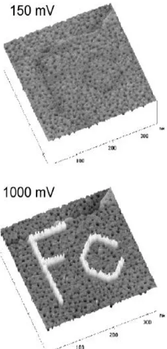
Figure 1.6. Replacement lithography images showing an electroactive FcC11S replaced into a C12S-SAM. Also illustrated is bias dependent apparent height contrast shown by the darkened Fc at 150mV and brightened Fc at 1000mV with a set point current of 10pA. Reprinted from reference 33. Copyright 2003,
American Chemical Society.………... 19
Figure 1.7. A series of replacement lithography experiments imaged by STM with FcC11S as replacing molecule and background monolayer indicated at the left side of each image. Each scanned image illustrates the effect of varying the applied bias within each monolayer while maintaining constant humidity ~55% and writing speed 20nm/s. Reprinted from reference 45.
Copyright 2004, American Chemical Society.………... 20
Figure 2.1. Cyclic voltammograms of desorption responses for C8S-SAM
on (A) gold and (B) platinum. The potential was scanned at 20 mV/s in 100µM C8SH / 0.1 M KOH/Ethanol
solution..………... 31
Figure 2.2. Cyclic voltammograms of the faradic responses of ferricyanide ion at C12S-SAMs on (A) gold, (B) platinum, and (C) palladium substrates as the monolayer is reductively desorbed from the surface. The potential was scanned at 100 mV/s in 10 mM K3Fe(CN)6/1M KNO3. Some of the curves are annotated with the potential at which the electrode was held prior to obtaining the faradaic response of the ferricyanide ion. The faradaic response monotonically increased as the holding potential of the
electrode became more negative. ………... 32
Figure 2.3. Desorption profiles of ▲C12S-SAM, ● C10S-SAM, ■ C8S-SAM on (A) gold, (B) platinum, and (C) palladium substrates. Each point represents an average of three trials and error bars are 90% confidence intervals. Lines represent Boltzmann Sigmoidal fits of the data and are drawn in solid blue lines for C12S-SAM, dashed red lines for C10S-SAM, and dash-dotted black lines for C8S-SAM desorption profiles. Derivatives of
ix
Figure 2.4. Representation of 20%, 50%, and 80% of total desorption (e.g. maximum faradaic response of ferricyanide) versus alkyl chain length of the SAM (with linear fit to the three points) on ■ gold (solid line), ▲ platinum (dashed line), and ● palladium
(dotted line). ………... 37
Figure 2.5. Removal of a dodecanethiolate SAM from gold due to RD (solid lines) and readsorption via OA (dotted lines) as the
potential of the desorbing solution was stepped to more negative potentials and more positive potentials, respectively. These experiments were performed in (A) 100 µM dodecanethiol and (B) 250 µM dodecanethiol. These data were fit to Boltzmann Sigmoidal functions as in Figures 2.3 A-C and derivatives of these fits are shown for (C) 100 µM dodecanethiol and (D) 250 µM dodecanethiol analogous to the data in
Figures 2.3 D-F.………..………... 41
Figure 2.6. Removal of a dodecanethiolate SAM from platinum due to RD (solid lines) and readsorption via OA (dotted lines) as the
potential of the desorbing solution was stepped to more negative potentials and more positive potentials, respectively. The protocol for the experiments and the format of these data are identical to
those shown in Figure 2.5. ………... 43
Figure 2.7. Redox response of potassium cyanide (under the same conditions reported in Figure 2.2) on (solid line) PtOx and (dashed line)
bare Pt prepared as described in the text..………. 45
Figure 3.1. Schematic illustrating the process of replacement lithography. ………... 51
Figure 3.2. STM images of replacement lithography on gold, palladium, and platinum (the pattern indicates the metal). The molecule
Fc-C11SAc was replaced into a C12S-SAM. Imaging conditions: image sizes 125 X 125 nm; for Au and Pd, 1.7 V scan bias, 10 pA set-point current, and 3 nm Z range; for Pt, 1.9 V scan bias, 10 pA set-point current, and 3 nm Z range. RL conditions: ~55%
relative humidity and biases of 3.4, 3.1, and 3.55 V, respectively,
x
Figure 3.3. Graphs and STM images indicating the percentage of
Fc-C11SAc replacement versus replacement bias on C12S-SAMs on gold, palladium, and platinum. The images are annotated with the biases used to generate each line. Lines on the graphs are solely a guide to the eye. Imaging conditions: Vbias ) 1.7 V (Au, Pd) and 1.9 V (Pt); Iset ) 10 pA, Z-scale ) 3 nm, and XY-scale ) 300 nm X 150 nm. Error bars shown represent the magnitude of
the 95% confidence interval of the data.………... 54
Figure 3.4. Graphs of percentage of Fc-C11SAc replacement versus replacement bias on C12S-SAMs on unetched platinum and palladium. The STM image (inset) is of a C12S-SAM on palladium imaged at 1.0 V, set-point 10 pA, scan size 400 nm2, and Z-scale 3 nm. Error bars shown represent the magnitude of the 95% confidence
interval of the data.………..……….. 55
Figure 4.1. Graph of apparent height versus Line Number of Ferrocene-C11S- Au on a C12S-Au background monolayer. Inset shows an STM image which is actually that of a single line that is repeatedly scanned. Scan biases are listed next to the corresponding
line number.……….……... 66
Figure 4.2. Variation in apparent height versus applied bias for a line of Fc-C11-SAc replaced into a C12S-Au background SAM at a constant set point current of 10 pA. Inset shows a series of representative STM images of the same line that were used to
generate the graph. ………... 67
Figure 4.3. STM images that track single lines of replaced molecules. (A) Fc-SAc on replaced into a C12S-SAM on gold, (B) Fc-NC replaced into a C12S-SAM on on gold, (C) Fc-SAc replaced into a C12S-SAM on on platinum, and (D) Fc-NC replaced into a C12S-SAM on on platinum. Underneath the images are labeled indicating the scan bias at which each line
was imaged.………... 68
Figure 4.4. Graphs of apparent height of either ferrocenyl thiol or isonitrile lines versus applied bias. Each set of data are fit to a Boltzmann sigmoid fit, and a grey dashed line is provided to indicate the
xi
Figure 4.5. Graphical representative derived of the statistical fits from Figure 4.4 with (A) Fc-SAu,(B) Fc-NCAu, (C) Fc-SPt, and (D) Fc-NCPt. Vertical lines are added to guide the eye to
peak positions. ………... 71
Figure 5.1. STM images that track the apparent height of lines of C10NC replaced into in dodecanethiolate SAMs on gold and platinum
substrates………... 80
Figure 5.2. Schematic showing process used to quantify the apparent height contrast for each STM image collected: (A) raw image; (B) fit
to a sum of two Gaussians……….81
Figure 5.3. Graphs of apparent height of (A) C8NC-Au, (B) C10NC-Au, (C) C12NC-Au, (D) C8NC-Pt, (E) C10NC- Pt, and (F) C12NC-Pt.
Each set of data was fit with a Boltzmann sigmoid fit.………... 82
Figure 5.4. Graphical representation of derivates taken of Boltzmann fits from Figure 5.2 (A) C8NC-Au, (B) C10 NC-Au, (C) C12 NC-Au, (D) C8NC-Pt, (E) C10NC- Pt, and (F) C12NC-Pt. A vertical
line at the peaks was added to guide the eye. ………... 83
Figure 5.5. Graphs of IR data for isonitriles synthesis with C8NC represented by the solid line response, C10NC the dashed line, and C12NC
the dotted line……….………... 86
Figure 6.1. STM images that track areas of Adventitious Replacement. Fc-SAc replaced into a C12S-SAM on gold with the
concentrations of Fc-SAc listed on top of the images and
the time each image was taken listed at its side. ………... 92
Figure 6.2. Graphs representing the percentage of adventitious replacement of Fc-SAc overtime taken at various concentrations: (A) 10 µM,
(B) 25 µM, (C) 50 µM, and (D) 100 µM……….………….. 93
Figure 6.3. Graphs of background monolayer versus adventitious replacement overtime fit with exponential functions. Concentrations for each graph labeled as (A) 10 µM, (B) 25 µM, (C) 50 µM, and
xii
LIST OF TABLES
Table 5.1. Peak positions extracted from the derived sigmodial fits by chain
length..………...83
Table 6.1. Rate constants listed by concentrations from exponential fits in
1
Chapter 1
Patterned Self Assembled Monolayers via Scanning Probe Lithography
2
1.1.Introduction
Upon looking back into human history one finds diverse forms of lithography to
communicate ideas and creeds. The substrates include cave walls, tablets, and canvas
used for paintings, carvings, and diverse forms of writing and art. Each of these
substrates requires a different form of lithography: the process of elimination for carving
or the process of addition for painting and writing.
In tracing the development of each form of lithography, the simplest and most
useful means of fabrication dominated the earliest efforts. Initially the use of a series of
markings on individual tools allowed the identification and possession of personal
effects. The concept of elimination lithography rests on the precept that features removed
from the surface are fabricated through a series of scratches. This system only requires a
flat surface and a sharp rock, much like some current nanolithography schemes.
These techniques can be translated into the modern day areas of nanolithography
through the use of scanning probe lithography. With scanning probe lithography it is
possible to remove material from the substrate via elimination or add to the surface via
addition or do both via substitution. Each of these methods have there own unique
advantages and disadvantages which will be discussed in the proceeding chapter.
The purpose of this chapter to illustrate the abilities of scanning probe microscopy
in the modification of various substrates based on self-assembled monolayers. A
3
more complete coverage of this subject.1 The main substrate that will be discussed in
this chapter is that of alkyl thiolate monolayers on single crystalline gold substrate.
Through the examples provided here, it will emerge that this system is one of the most
robust and flexible on this length scale. These properties account for its ubiquitous use in
nanometer-scale lithography.
1.2.Elimination Lithography
Elimination lithography can be thought of as the oldest form of writing beginning
with the ancient cultures carving symbols into stone more than 4000 years ago. Today
our techniques are more sophisticated but they are based on the same principle of
removing material to create patterns.1,2 Line resolution using elimination lithography
varies with the substrate and monolayer with the highest resolution being near 10
nanometers. The first example of probe-based elimination lithography employed a
scanning tunneling microscope (STM).3-6 Crooks et al created geometrically well defined
structures with a range of dimensions from 60 nanometers (nm) to 5 micrometers (µm).
This was accomplished by first preparing a gold bead in a dihydrogen flame in order to
form a faceted Au (111) surface. The faceted surface was then exposed to a 1 millimolar
ethanolic solution of octadecanethiol for 24 hours. The smaller features of circa 60 nm
were fabricated by elevating the tip bias to 3 volts while the larger 5 µm regions were
obtained by using a more substantial 8 volt tip-sample bias. The measured thickness of
the patterns, 0.7 nm, was not equal to the ellipsometric thickness of the
4
To address this apparent disparity in thickness, the authors used Ru(NH3)6+3 to
electrochemically probe the 5 square micron patterns to determine the surface coverage.
These measurements resulted in the same amount of current passed through the bare
feature as that obtained from a probe with a radius of 3.6 µm. Moreover, the current
scaled with the number of patterned features present. These findings led the authors to
conclude that they were indeed removing the octadecanethiolate monolayer and that the
disparity between scan line measured depth and ellipsometrically measured thickness of
the SAM was a reflection of the different conductances through the SAM-covered and
bare regions.3 Thus, as probed by STM, the SAM appeared taller relative to the
5
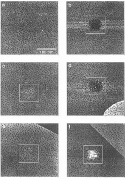
Figure 1.1. 300nm X 300nm scanned image via STM of an n-octadecyl mercaptan SAM with a
centralized 50nm X 50nm patterned region fabricated under varying relative humidity from ~75% for images (a), (b), (d), and (f) and ~6% for (c) and (e). Also the imaged surface in (a) represents a prepatterned surface; where as, (b)-(e) contain the patterned feature at a bias of 3.0V and (f) at -3.0V. Reprinted from reference 5. Copyright 1996, American Chemical Society
The mechanism of this transformation is postulated to be electrochemical in
nature.3-6 This conjecture has been supported by the results of experiments in which the
ability to desorb a monolayer with increased tip-substrate bias was directly related to the
relative humidity (Figure 1.1).3-6 To establish this relationship, Crooks et al. investigated
the influence of relative humidity on the desorption of n-octadecane thiolate monolayers
6
while the relative humidity was controlled. A higher relative humidity facilitated the
process. Interestingly, the application of a reverse bias failed to desorb the monolayer;
instead it appeared that material from the tip deposited onto the surface.
One impetus for studying the desorption of SAMs was based on the idea that they
could be well-controlled, ultrathin resists. To this end, Craighead et al. investigated the
use of an etched tungsten STM tip as a source for low energy electrons to modify a
surface of an octadecanethiolate SAM grown on both gold and gallium arsenide (GaAs).
Using the SAM/gold system they were able to create lines with a resolution limit of 25
nm. Using the SAM/GaAs system, 20 nm lines were produced as determined by AFM.
Lithography on both the gold and the GaAs systems resulted in raised features unless the
current and voltage values were sufficiently high/low respectively to cause the tip to
contact the surface and mechanically remove the monolayer.7
Elimination lithography on self-assembled monolayers has also been performed
with AFM.8 AFM is particularly suited for elimination lithography because, unlike in
STM, the tip in contact mode AFM is known to be in mechanical contact with the
monolayer and thus presumably can mechanically disrupt the SAM at elevated setpoint
force. It may be the case, however that the tip mechanically disrupts the SAM in STM as
well.2,9 The first example of elimination lithography on a SAM with AFM was shown on
alkanethiolate monolayers on gold.8 In this example, while scanning over a region, the
applied tip force was increased and local degradation of the monolayer was noted.8
7
stranded DNA10 and single-stranded DNA11 from gold.
Another example of elimination lithography on SAMs has been performed using
current sensing atomic force microscopy (CS-AFM)12 also known as conducting probe
AFM (CP-AFM).13 The CS-AFM has the capabilities of normal AFM combined with
current sensing abilities similar to that of STM.2 The instrument allows the simultaneous
measurement of the surface topography and I-V curves and has the advantage being able
to determine the lateral location of the tip with respect to various domain and other
topographic features associated within the monolayer with a high degree of precision.13,14
Using CS-AFM, Uosaki, et al. were able to remove an octadecanethiolate monolayer
from beneath the tip by applying a bias between the tip and substrate. This removal was
indicated by an increased current in lithographically patterned regions of SAM as well as
topographical depressions with a depth corresponding to that of the thickness of the
SAM.12 Further experiments into the elimination mechanism of this technique illustrated
that the bias required to remove the SAM was dependent on relative humidity15 as had
been observed previously by Crooks et al.6
Anodic oxidation of silicon has frequently been employed as an elimination
lithography technique.1 In this process the CS-AFM tip was contacted with the silicon
wafer through a water meniscus. Upon application of a bias, the monolayer, generally
trimethylsilyl (TMS), was removed and the underlying silicon was hydrolyzed to
Si-OH.15,16 The patterned silicon wafer was then exposed to an etching solution. The
8
Similar anodic oxidation experiments were performed in which an octadecylsiloxane
(ODS) monolayer was oxidized, an amine terminated silane was introduced and self
assembled onto the patterned area. Gold nanoparticles were then trapped in these
regions.17 Several other very interesting experiments were shown in which single gold
colloids were trapped18, surface charge versus applied bias was tested19, and alkyl
monolayers were patterned.20
1.3.Addition Lithography
The second oldest form of writing and perhaps the oldest form of artwork is that
of addition lithography. Addition lithography is based on a concept that is very familiar
to society, writing with an ink on blank paper. There are several different methods for
patterning monolayers using micropens, nanopipets, and microcontact printing (μCP)1,21
With respect to the use of a probe tip, one finds the use of AFM for this type of writing.
Since the feedback signal in STM is current, and any material on the tip will have a large
influence on tunneling probability, the idea of an inked tip is not amenable to STM.
Hurley et al. described a form of addition lithography in which alterations of the
initial Si-H terminated monolayer were made through the application of a bias on a
conductive-AFM probe.22 In this procedure, termed electrografting, alkyne terminated
molecules produced a surface conducive to silylation chemistry in which Si-C bonds
formed within the 40nm patterned lines (Figure 1.2). A variation in height and friction
occured in the regions of electrografted molecules. Upon imaging the surface after
9
revealed height variations consistent with the length of the grafted molecules.
Dip-pen nanolithography (DPN) employs an AFM tip coated with some material
as a writing implement on a surface.23 In DPN an AFM tip is “inked” with a solution that
will self assemble or otherwise adhere onto the surface of choice. The tip is then brought
into contact with the surface at which point a water meniscus is formed which is believed
to facilitate in the transportation of the ink from the tip to the substrate. Since the first
example of DPN24 this procedure has been used in both tapping and contact mode to
pattern various substrates from gold and mica to silicon and gallium arsenide with inks
ranging from alkyl thiols to proteins.23
Figure 1.2. (a) 1-octadecyne, (c) 1-dodecyne, and (e) 1,4-diethynylbenzene electrografted patterned on hydride
terminated Si with the top row being height images and the corresponding bottom frictional images (b), (d), and (f) respectively. Reprinted from reference 22. Copyright 2003, American Chemical Society.
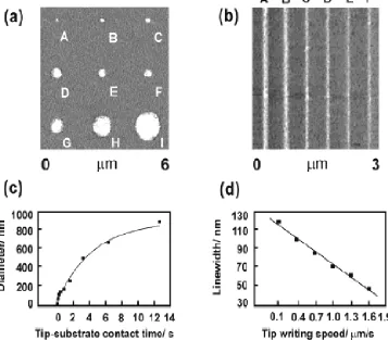
In one interesting example, Liu and coworkers explored the use of magnetic
10
mercaptohexadecanoic acid, MHA.25 The fabrication of magnetic nanostructures has
implications in various fields such as the development of magnetic storage devices which
increase in capacity as the density of magnetic features increase. Liu et al. created
magnetic structures via DPN by patterning MHA on a gold substrate then immersing in a
1-octadecanethiol, ODT solution to back-fill the remaining bare gold regions. The
sample was then dipped in nanoparticle solution. To characterize the fabrication process,
various stationary exposure times of the cantilever to the substrate as well as writing
speeds were recorded for the initial formation of MHA monolayers followed by
previously established procedures. Notably Liu et al. observed that the variation of
contact time and writing speed generated two different behaviors. The feature size as a
function of contact time produced a nonlinear response that differed when compared to
the variation of writing speed (Figure 1.3). However, most notable was the facilitation
of nanoparticle attachment to MHA-covered regions of the surface but not to
11
Figure 1.3. (a) An array of features scaling from 45nm- 920nm in diameter generated by varying the
contact time during the MHA writing phase with contact time increasing from A-I backfilled with ODT and developed with magnetic nanoparticles. (b) Lines produced by varying writing speeds from 0.1µm/s to 1.3µm/s creating line widths of 120nm to 60nm scaled from A-F. (c) A study of contact time versus feature diameter plotted via analysis of (a). (d) A plot of writing speed compared to fabricated line widths produced in (b). Reprinted from reference 25. Copyright 2002, WILEY-VCH Verlag GmbH.
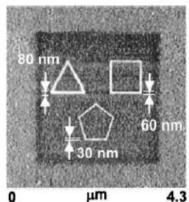
Hong and coworkers examined the feasibility of patterning multiple “inks” with
DPN.26 In their investigation, the application of multiple inks required the use of a closed
loop AFM. Closed loop AFM allowed the use of alignment markers to ensure more
accurate alignment and positioning of the AFM tip. The features observed (Figure 1.4)
were produced as a result of patterning MHA at a writing speed, the variation of which
12
exchanged with an ODT coated one, and rastering the tip over a 3µm size square resulted
in a backfilling with the ODT to create the darkened region surrounding the geometric
features. The precision of line placement, control of thermal drift (>1nm/min), and
application of multiple inks onto a single substrate provides avenues into exploring and
comparing multiple SAMs simultaneously.
Figure 1.4. Polygons written with MHA preformed with varying writing times. The darkened square 3µm
x 3µm region was patterned afterwards by writing with ODT. Reprinted from reference 26. Copyright 1999, American Association for the Advancement of Science.
Another interesting use for DPN is for the creation of templates. This method
involves patterning the surface with a substituent that will bind the “material of interest”.
13
There are several questions that still exist on the fundamental mechanism that drives
DPN. The mechanism of ink transport by the water meniscus is one of these questions.
Another is the method by which hydrophobic molecules are transferred through this
water meniscus, and yet another focuses on the need for the water meniscus. To date the
answers to these questions are still up for speculation with some arguing both for28 and
against29 the necessity of the water meniscus. These experiments and their interpretation
are reviewed in more detail elsewhere.1,23
1.4.Substitution Lithography
The third form of writing is that of substitution lithography where first the
background canvas is removed and then replaced with a second type of ink. Substitution
lithography is based upon the ability to remove an existing monolayer and replace it with
another in the removal region.1 The advantage of this approach is that it retains a
chemical identity in all regions on the substrate and allows the comparison of two or
more different SAMs simultaneously.30
In an early example, this method was used to pattern monolayer protected gold
with a thin layer of silver by elevating the bias of a silver coated platinum iridium tip
over a scanned region of the monolayer. Upon elevating the bias the monolayer was
removed and the silver was deposited. Subsequent scanning over the region revealed that
no silver had been deposited outside of the scan area.31
14
dodecanthiolate monolayer.30 In this experiment a low current STM was used to remove
the dodecanethiolate monolayer in a dodecane solution containing decanethiol.
Interestingly upon replacement the decanethiolate replaced regions illustrated a higher
apparent height as compared to the dodecanethiolate background. This reversed apparent
height contrast was attributed to the tunneling gap of the dodecane solution having a
higher conductance than the monolayer as had been predicted previously.32
This technique has also been employed to create monolayers composed of both
insulating and electroactive regions by removing lines from a dodecanethiolate
background in a solution of ferrocenylundecanethioacetate (Fc-C11-SAc) and three
component monolayers consisting of two electroactive regions separated by the insulating
dodecanethiolate background.33
Another interesting experiment performed with this technique was the creation of
chemical gradients in which a Fc-C11SH gradient was fabricated into a dodecanethiolate
monolayer and a mercaptoundecanoic acid gradient was fabricated into a
dodecanethiolate monolayer.34 Examples of substitution lithography have also been
illustrated with CS-AFM in which hexanethiol, octanethiol and decanethiol were replaced
into a monolayer of octadecanethiolate.35
AFM can also be used to remove the monolayer in a solution of replacement
thiol.36 Interestingly the patterns produced by this method (termed „nanografting‟) form at
least one order of magnitude faster and have fewer defect sites than monolayers formed
15
nanografting both in situ and ex situ. One interesting example of ex situ patterning was
the binding of protein to nanografted areas of mercaptopropionic acid in a
dodecanethiolate background.38
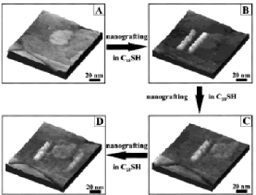
Figure 1.5. (A) An AFM image of C10S SAM prior to fabrication. (B) Patterning of two 10 nm x 50 nm
C18S lines with 20 nm spacing. (C) Removal of one of the C18S lines and reintroduction of the C10S into
the region. (D) Fabricating another C18S line 65nm in length. Reprinted from reference 39. Copyright
1999, American Chemical Society.
Early studies performed by Xu and Liu utilized the mechanical attributes of AFM
in order to displace “matrix monolayer” components from substrates. Through the
application of an increase in scanning force nanoshaving36 was observed as they had
previously reported. However, with the addition of C12SH or C10SH in supporting
solution it was observed that the replacing “ink” adsorbed into the freshly etched regions.
16
nanografting, the ability to “erase” lines fabricated within the monolayer as well as
reform them demonstrated a vast range of control in the selectivity of structural
manipulation through AFM.39 Also, structures fabricated through this methodology
illustrated control in line resolution, given the reproducible 10 nm line width and 50 nm
length. Formation of lines with these dimensions resulted from the application of 5.2nN
setpoint force during the writing scan with 0.1mM of replacing molecules in 2-butanol
solution. In order to confirm the replacement of the monolayer imaging scans taken with
a 0.3nN setpoint force observed the change in relative height of the replaced region. The
expected difference in lengths of that of the C18S and C10S molecules suggested the
complete replacement of the monolayer in the selected region.
A second classification of substitution lithography is tip induced modification of
the terminal head group in the SAM.1 In this process, the underlying chain is left
unperturbed with only the chemical functionality of the terminal headgroup affected.
STM, AFM and CS-AFM have been used in this process. An interesting example is the
chemical modification of an amine terminated organosilane by the low energy electron
beam of a STM.40 After exposure to the low energy electrons from the STM tip the
functionality of the exposed surface was destroyed and therefore would not ligate ions in
subsequent steps. The undamaged regions were then exposed to aqueous Pd+2 followed
17
unexposed regions and the nickel plated only on the Pd+2 regions.40
In another example, CS-AFM was used to induce an nanoelectrochemical
oxidation of the terminal methyl group of a n-otcadecyltrichlorosilane monolayer.41 After
oxidation of the terminal methyl group, the sample was reacted with a vinyl terminated
silane which created a bilayer in the oxidized region. The vinyl group could then be
reacted to form various other terminal groups and further layers or functionalities could
be added. These examples indicate that substitution lithography on SAMs is another
useful method along with addition lithography and elimination lithography in preparing
and manipulating the components at a monolayer substrate interface.
1.5.Apparent Height
The ability to distinguish and characterize regions of replacement relies on the
properties of replacing molecules compared to that of the background SAM. Through the
use of STM and AFM several distinctive measurements are possible. The use of relative
heights and conductance measurements provide information into the structural and
electrical properties of regions in the SAM. Apparent height contrast, the relative
difference between two distinct regions of the SAM, provides both a visual representation
of replacement domains as well as comparative height measurements. In exploring the
relative conductance and height differences several factors contribute towards providing
clear-cut responses including the length and relative tilt of the molecules in the replaced
region, and how the relative conductance of the tip-molecule-substrate junction varies
18
Bias dependent apparent height contrast is based upon molecules having a
nonlinear increase in tunneling current as the tip-sample bias is increased. For example,
Gorman et al. demonstrated that a ferrocenyl-terminated SAM region shows little or no
apparent height contrast with the background dodecanethiolate SAM at a 150 mV
setpoint bias. However if the bias was increased to 1000 mV then the
ferrocenyl-terminated regions appeared much taller than the C12 background (Figure 1.6).33 The
mechanism behind this apparent height contrast is suggested to be resonant tunneling.42
Resonant tunneling occurs when the Fermi energy levels in the tip and a suitable level of
the redox active molecule come into alignment. At low potentials the Fermi level of the
tip is too low to access a molecular orbital associated with the molecule and therefore
little excess tunneling current is observed. However, if the Fermi level of the tip is
brought into alignment with a MO on the molecule the tunneling current increases
dramatically and an apparent height difference is seen between the insulating background
and the electroactive molecule. This effect has been modulated by installing the
electroactive groups reversibly using non-covalent interactions43 and by capping the
19
Figure 1.6. Replacement lithography images showing an electroactive FcC11S replaced into a C12S-SAM.
Also illustrated is bias dependent apparent height contrast shown by the darkened Fc at 150mV and
brightened Fc at 1000mV with a set point current of 10pA.Reprinted from reference 33. Copyright 2003,
American Chemical Society.
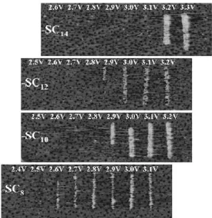
The ability to characterize SPL fabrication relies on the interpretation of the
surface features formed during the process. In an attempt to characterize the process of
replacement lithography Lewis and Gorman characterized the efficacy of replacement
based on the apparent height response.45 In doing so, the establishment of visible and
measurable desorption trends based on the length of the initial monolayer were
20
Figure 1.7. A series of replacement lithography experiments imaged by STM with FcC11S as replacing molecule and
background monolayer indicated at the left side of each image. Each scanned image illustrates the effect of varying the applied bias within each monolayer while maintaining constant humidity ~55% and writing speed 20nm/s. Reprinted from reference 45. Copyright 2004,American Chemical Society.
1.6.Concluding Thoughts
The field of scanning probe lithography on self-assembled monolayers has
evolved quickly and has already enjoyed utility in a materials science and life science
investigations. As this work continues to progress, we hopefully will learn more about
the mechanisms of these lithographic operations. Moreover, we will undoubtedly see a
further expansion of the range of investigations where nanopatterning of this type is
21
1.7.References
(1) Krämer, S., Fuierer, R. R., and Gorman, C. B., Chemical Review. 103 (11), 4367 (2003).
(2) Soh, H. T., Guarini, K. W., and Quate, C. F., Scanning Probe Lithography. (Kluwer Academic Publishers, Boston, 2001).
(3) Ross, C. B., Sun, L., and Crooks, R. M., Langmuir 9 (3), 632 (1993).
(4) Schoer, J. K., Ross, C. B., Crooks, R. M. et al., Langmuir 10 (3), 615 (1994).
(5) Schoer, J. K., Zamborini, F. P., and Crooks, R. M., Journal of Physical Chemistry. 100 (26), 11086 (1996).
(6) Schoer, J. K. and Crooks, R. M., Langmuir 13 (8), 2323 (1997).
(7) Lercel, M. J., Redinbo, G. F., Craighead, H. G. et al., Applied Physics Letters. 65 (8), 974 (1994).
(8) Liu, G. Y. and Salmeron, M. B., Langmuir 10 (2), 367 (1994).
(9) Touzov, I. and Gorman, C. B., Journal of Physical Chemistry B. 101, 5263 (1997).
(10) Kelley, S. O., Barton, J. K., Jackson, N. M. et al., Langmuir 14 (24), 6781 (1998).
(11) Zhou, D. J., Sinniah, K., Abell, C. et al., Langmuir 18 (22), 8278 (2002).
(12) Zhao, J. W. and Uosaki, K., Langmuir 17 (25), 7784 (2001).
(13) Wold, D. J. and Frisbie, C. D., Journal of the American Chemical Society. 123 (23), 5549 (2001).
(14) Wold, D. J. and Frisbie, C. D., Journal of the American Chemical Society. 122 (12), 2970 (2000); Leatherman, G., Durantini, E. N., Gust, D. et al., Journal of Physical Chemistry B. 103 (20), 4006 (1999); Rawlett, A. M., Hopson, T. J., Nagahara, L. A. et al., Applied Physics Letters. 81 (16), 3043 (2002).
(15) Sugimura, H., Okiguchi, K., Nakagiri, N. et al., Journal of Vacuum Science Technology. B 14 (6), 4140 (1996).
(16) Sugimura, H. and Nakagiri, N., Langmuir 11 (10), 3623 (1995).
(17) Zheng, J. W., Zhu, Z. H., Chen, H. F. et al., Langmuir 16 (10), 4409 (2000).
(18) Li, Q. G., Zheng, J. W., and Liu, Z. F., Langmuir 19 (1), 166 (2003).
(19) Kim, S. M., Ahn, S. J., Lee, H. et al., Ultramicroscopy 91 (1-4), 165 (2002).
22
(21) Xia, Y. N., Mrksich, M., Kim, E. et al., Journal of the American Chemical Society. 117 (37), 9576 (1995); Koide, Y., Such, M. W., Basu, R. et al., Langmuir 19 (1), 86 (2003); Jun, Y., Le, D., and Zhu, X. Y., Langmuir 18 (9), 3415 (2002).
(22) Hurley, P. T., Ribbe, A. E., and Buriak, J. M., Journal of the American Chemical Society. 125 (37), 11334 (2003).
(23) Ginger, D. S., Zhang, H., and Mirkin, C. A., Angewandte Chemie International Edition. 43 (1), 30 (2004).
(24) Piner, R. D. and Mirkin, C. A., Langmuir 13 (26), 6864 (1997); Hong, S. H., Zhu, J., and Mirkin, C. A., Langmuir 15 (23), 7897 (1999); Piner, R. D., Zhu, J., Xu, F. et al., Science 283, 661 (1999); Hong, S. H., Zhu, J., and Mirkin, C. A., Science 286 (5439), 523 (1999).
(25) Liu X., F. L., Hong S., Dravid V. P., Mirkin C. A., Advanced Materials. 14 (3), 231 (2002).
(26) Hong S., Z. J., Mirkin C. A., Science 286, 523 (1999).
(27) Lee, K. B., Park, S. J., Mirkin, C. A. et al., Science 295 (5560), 1702 (2002); Smith, J. C., Lee, K. B., Wang, Q. et al., Nano Letters. 3 (7), 883 (2003).
(28) Rozhok, S., Piner, R., and Mirkin, C. A., Journal of Physical Chemistry B. 107 (3), 751 (2003).
(29) Schwartz, P. V., Langmuir 18 (10), 4041 (2002); Sheehan, P. E. and Whitman, L. J., Physics Review Letters. 88 (15) (2002).
(30) Gorman, C. B., Carroll, R. L., He, Y. F. et al., Langmuir 16 (15), 6312 (2000).
(31) Zamborini, F. P. and Crooks, R. M., Journal of the American Chemical Society. 120 (37), 9700 (1998).
(32) Weiss, P. S., Bumm, L. A., Dunbar, T. D. et al., Ann. N. Y. Academy of Science. 852, 145 (1998).
(33) Gorman, C. B., Carroll, R. L., and Fuierer, R. R., Langmuir 17 (22), 6923 (2001).
(34) Fuierer, R. R., Carroll, R. L., Feldheim, D. L. et al., Advanced Materials. 14 (2), 154 (2002).
(35) Zhao, J. W. and Uosaki, K., Nano Letters. 2 (2), 137 (2002).
(36) Xu, S. and Liu, G. Y., Langmuir 13 (2), 127 (1997).
(37) Xu, S., Laibinis, P. E., and Liu, G. Y., Journal of the American Chemical Society. 120 (36), 9356 (1998).
(38) Browning-Kelley, M. E., Wadu-Mesthrige, K., Hari, V. et al., Langmuir 13 (2), 343 (1997); Wadu-Mesthrige, K., Xu, S., Amro, N. A. et al., Langmuir 15 (25), 8580 (1999).
(39) Xu, S., Miller, S., Laibinis, P. E. et al., Langmuir 15 (21), 7244 (1999).
23
(41) Maoz, R., Frydman, E., Cohen, S. R. et al., Advanced Material. 12 (10), 725 (2000).
(42) Tao, N. J., Physical Review Letters 76 (21), 4066 (1996).
(43) Credo, G. M., Boal, A. K., Das, K. et al., Journal of the American Chemical Society 124 (31), 9036 (2002).
(44) Wassel, R. A., Credo, G. M., Fuierer, R. R. et al., Journal of the American Chemical Society. 126, 295 (2004).
24
Chapter 2
Alkanethiol Reductive Desorption from Self-Assembled Monolayers
on Gold, Platinum, and Palladium Substrates
This work appeared in print: Williams, J. A.; Gorman, C. B. Journal of Physical
Chemistry C, 2007, 111, 12804-12810.
Acknowledgement is given to Marc Porter for helpful discussions and Jennifer Ayres,
25
Abstract
The reductive desorption of n-alkanethiolate self-assembled monolayers (SAMs)
on gold, platinum, and palladium substrates were investigated. The kinetics of this
process were too slow to measure directly in the case of RS-Pt and RS-Pd SAMs. Thus,
the Faradaic response of potassium ferricyanide after partial or complete desorption was
determined and used to quantify the relative electrochemically accessible surface area.
Both the type of underlying metal substrate and the chain length of the n-alkane thiol
were varied. The relative alkanethiol binding affinity and effective kinetics of binding
for each of the substrates were discussed in light of these observations.
2.1. Introduction
Controlling the interaction between molecules and a surface is fundamental to the
creation of self-assembled monolayers (SAMs). Ideally, molecules can be both attached
to and released from a surface. This behavior has existing and potentially new uses in a
variety of fields including the creation of dynamic interfaces for biomolecular and
cellular attachment,1,2 dynamic control of monolayer composition,3-6 and electronic
phenomena at a surface.7,8 This is particularly relevant when considering the stability of
metal-molecule junctions (or, conversely, using an applied potential to alter the junction).
In the case of SAMs of organo thiolates on gold, molecular release can take place
by the process of reductive desorption (RD). Porter et al. first reported this phenomenon
26
the surface.9,10 The mechanism proposed was a single electron reduction of the surface
bound species to form a thiolate in solution.
Variation of the metal substrate upon which molecules are attached and released
would be attractive in the investigation of several current research questions. For
example, many molecular devices involve a redox active molecule between two Au
electrodes. It has been shown that the tunneling barrier to electron transport between the
metal and the molecule varies substantially with the metal chosen.11 However, the RD
process on SAMs with substrates other than Au and Ag9,12,13 has yet to be fully explored.
Azzaroni et al. showed that the electrodesorption potentials for SAMs on copper are
shifted 0.6 V in the negative direction with respect to those found on Au.14 Several
studies have examined SAMs on mercury electrodes as well.8,15-17 By monitoring the
applied potential dependence of the surface coverage of electroactive osmium complexes
adsorbed on Au and Pt substrates Bretz et al. established a shift in the point of zero
charge (PZC) during the formation of the SAMs.18,19 These authors argued that the
adsorption of this charged, electroactive species was only facile above the PZC of the
electrode. Yang et al. studied the RD process on Pt(111) coated with organosulfur
adsorbates. However, potential excursion to the onset of water reduction in 0.1 M KOH
did not result in desorption, leading these authors to speculate that organosulfur
admolecules may be adsorbed more strongly on Pt(111) than on Au(111).20 Based on
these observations, it is not yet clear whether the process of RD of SAMs on Pt can take
27
Thus, these issues lead one to the question: can the process of RD be extended to
other metal/organothiolate structures and, if so, what are the relative kinetic and
thermodynamic parameters governing this process? In this work it will be shown that a
direct, voltammetric measurement of RD is not always possible. However, the current
response of a redox active probe (an electroactive species in solution with limited
permeability into the SAM) can be used to determine the extent of desorption and
structural state of the SAM. Via this approach, the relative thermodynamics of RD can
be assessed as a function of the chain length of the n-alkanethiolate SAM on the
substrate.
2.2. Experimental
Working Electrodes
Platinum, gold, and palladium bead electrodes where fabricated via flame
annealing of 0.5 mm diameter wire (99.99+% purity, Alfa-Aesar) of each metal. Au
beads were formed through the application of a hydrogen flame; after which the bead was
zone refined as preformed by Schoer21,22 and the impurities removed. This process was
repeated for 15 minutes to further separate impurities towards its base. Following the
zone refining the Au bead was immersed in freshly prepared Piranha solution (3 H2SO4 to
1 H2O2) for 3 minutes, and again zone refined as before. Platinum and palladium beads
underwent similar treatment with the exception that a hydrogen/oxygen flame was chosen
for melting and zone refining due to the higher melting point of these metals. In order to
28
as a result of the annealing process, was acid “etched” for 15 minutes (Pt) and 1 hour (Pd)
using concentrated H2SO4 and concentrated HCl respectively.
Monolayer Adsorption
All samples for electrochemical studies were prepared by placing the previously
prepared metal substrate in 1mM alkanethiol/ethanol solution and refluxing for one hour.
After cooling to room temperature, samples were incubated for at least an additional 24
hrs prior to experimentation. This process was repeated for each metal in ethanol
solutions of octanethiol, decanethiol, and dodecanethiol (Alfa Aesar).
Two-Step Desorption Study
After monolayer formation, the integrity of the monolayer was verified by
ensuring that the Faradaic CV of the redox peak of aqueous 10mM potassium
ferricyanide (K3Fe(CN)6)/1.0M potassium nitrate (KNO3) was less than 30 µA/cm2 at
230 mV, the cathodic peak maximum for ferricyanide. To successively remove the
SAM, the following procedure was employed. The substrate was alternated between a
0.1mM potassium hydroxide (KOH)/ethanol solution and the ferricyanide solution. Each
time the substrate was immersed in the KOH solution, the potential was held versus a
Ag/AgCl reference electrode for 30 seconds at an increasingly negative potential (-200,
-400,-450,-500,-800,-850,-900,-950,-1050 mV, and then -1100 to -3000 mV in 100mV
increments). After each treatment in KOH/ethanol, the substrate was transferred to the
29
Pt and Au and 0 to 500 mV for Pd. If care was not taken to remove the surface oxide
from Pt and Pd substrates as described above, significant variations in the response were
observed. In the case of palladium surfaces, little blocking was observed, suggesting that
a monolayer did not form.
2.3. Results and Discussion
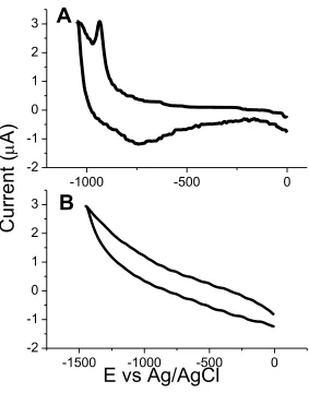
As stated above, observation of a desorption wave using cyclic voltammetry is
arguably the easiest way to characterize a RD process. Thus, our first attempt at studying
RD of SAMs on Pt substrates involved this process. SAMs of octanethiol (C8SH) on Pt
were prepared. These surfaces were annealed metal beads and thus presented
predominantly the (111) crystallographic face. They are not single crystalline and thus
this polycrystallinity is expected to introduce some variability (e.g. in the span of
electrochemical potential over which reductive desorption occurs). However, as most
nanometer-scale electrodes are prepared in a fashion that presents a similar surface, these
substrates and SAM desorption from them are relevant when considering metal-molecule
junctions in molecular electronics.
In attempt to measure electrochemical desorption of the SAM from the metal
surfaces, cyclic voltammograms were obtained. However, as shown in Figure 2.1, this
approach did not yield useful results. Although the desorption peak for a C8S-SAM from
Au was observable (Figure 2.1A), no corresponding desorption peak for a C8S-SAM on
30
DMF solution following the protocol reported by Schneider and Buttry.25 Variation of
the scan rate by over a decade in magnitude also did not yield improvement in the results.
From these data, it was concluded that either the RD process did not take place for
a C8S-SAM on Pt within this potential range (as suggested previously by Yang et al.)20
or, as we hypothesized, the kinetics of this process were too slow to monitor by CV. This
latter hypothesis has also been supported by some work by Bretz and Abruña in which
redox-active, osmium bipyridine-based SAMs were desorbed from platinum by repeated
electrochemical cycling.19 To distinguish these possibilities, an alternate method for
31
-1500 -1000 -500 0
-2 -1 0 1 2 3
-1000 -500 0
-2 -1 0 1 2 3
E vs Ag/AgCl
B
C
u
rr
e
n
t (
A)
A
Figure 2.1. Cyclic voltammograms of desorption responses for C8S-SAM on (A) gold and (B) platinum.
32
Figure 2.2. Cyclic voltammograms of the faradic responses of ferricyanide ion at C12S-SAMs on (A) gold,
(B) platinum, and (C) palladium substrates as the monolayer is reductively desorbed from the surface. The
potential was scanned at 100 mV/s in 10 mM K3Fe(CN)6/1M KNO3. Some of the curves are annotated with
the potential at which the electrode was held prior to obtaining the faradaic response of the ferricyanide ion. The faradaic response monotonically increased as the holding potential of the electrode became more negative.
In an attempt to compensate for the proposed slow kinetics of desorption, the
desorption and subsequent examination of the relative surface coverage were separated
into two steps. First, the SAM-substrate was placed into a 0.1M KOH/ethanol solution
and held at a given potential for 30 sec. This sample was then removed and placed into
0 100 200 300 400 500 600 700
-2500 0 2500
E vs. Ag/AgCl (mV)
0 100 200 300 400 500 600 700
-2500 0 2500
Current per Area (
A/cm
2
)
-600mV -1200mV 0mV0 100 200 300 400 500 600 700
33
an aqueous solution of 10mM K3Fe(CN)6/1M KNO3. The relative amount of
reduction/reoxidation of the ferricyanide as compared to a bare surface was then used to
calculate the relative, electrochemically accessible area of the sample. This use of redox
active probes to characterize the relative coverage of a SAM has been reported
previously.26-28
Figure 2.2 shows a series of cyclic voltammograms that illustrate the faradic
response of K3Fe(CN)6 after each stage of RD on C12S-SAMs on Au, Pt, and Pd
substrates. Initially, CV’s were taken before any attempts at RD were made, and each
CV showed negligible faradaic response to ferricyanide. These results indicate that
dodecanethiol can form a high coverage, electrochemically blocking SAMs on each of
the three substrates. After holding the electrode at incrementally more negative
potentials in 0.1 M KOH/EtOH solution, subsequent CVs after the substrates were
returned to the ferricyanide solution showed incrementally greater Faradaic response.
The redox potential of ferricyanide was similar on each of these substrates, although the
kinetics of electron transfer on the Pd substrate were slower as evidenced by the greater
separation between the anodic and cathodic peaks. This result indicated that the SAM
was being progressively desorbed from the electrode. Moreover, in each case, the
potential in 0.1 M KOH/EtOH could be brought sufficiently negative so that eventually,
the Faradaic response of the ferricyanide was similar to that observed on a freshly
prepared, clean, bare substrate. Thus, it was concluded that the redox response of
34 substrates.
Using the ferricyanide redox probe, we then sought to address two questions.
First, does the potential of desorption vary with substrate? Second, how does the
potential of desorption vary with chain length for each substrate? To probe this, we
investigated the faradaic response of the electrochemically accessible surface area as the
RD occurred over applied potential steps. Data of the form obtained in Figure 2.2 was
acquired, and the peak current of the Faradaic response of the ferricyanide was used to
determine the electrochemically accessible surface area of the sample after each
increment of reductive desorption. This area was calculated using one of the two
equations shown below.
A= (ilim/4nFDC)2π (1)
A= ip/(2.69x105)n3/2D½ν½C (2)
Equation 1 was used when a sigmoidal CV response was obtained indicating
radial diffusion within a microelectrode system.29,30 In equation 1, ilim is the limiting
current measured, n is number of electrons transferred (assumed to be one for
ferricyanide/ferrocyanide), F is the Faraday constant, D is the diffusion coefficient for
potassium ferricyanide (D = 7.6 x 10⁻⁶ cm2/s), and C is the bulk concentration of
potassium ferricyanide (1 x 10⁻⁵ mol/cm3). Practically, this response was obtained for the
first ca. 10 % of the total desorption. Equation 2 (the Randles-Sevcik equation)31 was
employed when the CV response indicated a semi-infinite linear diffusion profile. In
35
values are as in equation 1. As the Faradaic response at the palladium electrode was
quasi-reversible and the Randles-Sevcik equation is strictly applicable for reversible
responses, it was verified that the error in using this equation was negligible by
comparing several of the values of the calculated area to those obtained by integrating the
area under the voltammogram to determine the charge passed. The areas obtained were
then divided by the total area obtained by voltammetry on the bare substrate to calculate
the percentage of desorption.
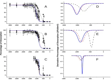
In this fashion, the desorption profiles of octanethiolate, decanethiolate and
dodecanethiolate SAMs on gold, platinum and palladium were obtained. The results are
shown in Figure 2.3. As the desorption profile appear sigmoidal in shape, each response
was fit to a Boltzmann sigmodial function. This treatment does not insinuate that this
response represents a Langmuir adsorption/desorption isotherm as it does not ensure that
each point obtained is a true equilibrium response. This issue is discussed in more detail
below. Further, the derivative of each function was computed and plotted in Figure
2.3D-F. These derivative functions permit an easier visual assessment of the range and
midpoint of the desorption profile. They are not, however, meant to be compared with
36
-3000 -2500 -2000 -1500 -1000 -500 0 0
25 50 75 100
A D
B E
C F
-1500 -1000 -500 0 -0.6 -0.5 -0.4 -0.3 -0.2 -0.1 0.0
-3000 -2500 -2000 -1500 -1000 -500 0 0 25 50 75 100 P e rc e n ta g e o f D e s o rp ti o n
-1500 -1000 -500 0 -0.6 -0.5 -0.4 -0.3 -0.2 -0.1 0.0 D e ri v a ti v e P e rc e n ta g e o f D e s o rp ti o n ( d % /d m V )
-3000 -2500 -2000 -1500 -1000 -500 0 0
25 50 75 100
Potential Held 30s in 1.0M KOH/EtOH (mV)
-1500 -1000 -500 0 -2.1
-1.4 -0.7 0.0
Figure 2.3. Desorption profiles of ▲C12S-SAM, ● C10S-SAM, ■ C8S-SAMon (A) gold (B) platinum and
(C) palladium substrates. Each point represents an average of three trials and error bars are 90% confidence intervals. Lines represent Boltzmann Sigmoidal fits of the data and are drawn in solid blue lines for C12S-SAM, dashed red lines for C10S-SAM, and dash-dotted black lines for C8S-SAM desorption
profiles. Derivatives of the fits on (D) gold (E) platinum and (F) palladium.
The range of desorption potential was 0 to -3000 mV for samples on gold and
platinum as the faradaic response increased or remained constant over this range. In the
case of the palladium substrate, at desorption potentials more negative than -1200 mV the
faradaic response began to decrease somewhat. Thus, these measurements were deemed
not to be a true quantification of surface area. Alkanethiolates self-assembled on
palladium are known to form a PdS interlayer.32 This interlayer could possibly be
37
the data presented here, the layer does not appear to strongly affect the redox kinetics of
the ferricyanide. As stated before, after removal of the SAMs at -1200 mV in
KOH/EtOH, the shape and magnitude of the ferricyanide response was similar to that on
bare palladium substrates.
8 10 12
-400 -600 -800 -1000
Alkane Chain Length
20 %
8 10 12
-600 -800 -1000 80 % P o te n ti a l o f D e s o rp ti o n ( m V ) 50 %
8 10 12
-600 -800 -1000 -1200
Figure 2.4. Representation of 20%, 50%, and 80% of total desorption (e.g. maximum faradaic response of
ferricyanide) versus alkyl chain length of the SAM (with linear fit to the three points) on ■ gold (solid line), ▲ platinum (dashed line), and ● palladium (dotted line).
The data in Figure 2.3 show that there is a chain length dependence on the
desorption of SAMs from each of the three substrates. Moreover, the desorption
response is different for each substrate. However, in this format, it is difficult to discern
either of these two types of differences. Thus, data from these fits were used to construct
38
total desorption occurred is graphed versus the alkyl chain length of the SAM. Linear fits
to these data are also provided to guide the eye.
The most notable feature of Figure 2.4 is the difference in slopes depending on
which percentage of desorption is chosen. This behavior reflects the relative broadness
of the sigmoids – desorption is not observed as a sharp event by this method. In contrast,
desorption potentials obtained from CV provide a discrete value. To state the potential
dependence of desorption as a function of substrate, one is faced with a scenario
complicated by the need to specify relative extent of desorption and chain length
dependence of desorption. However, a few general conclusions can be made from these
data.
At 20% desorption (e.g. closer to the onset), the relative ease as a function of
metal depends on the chain length of the SAM. However, it appears easiest to begin to
remove a SAM from platinum. Interestingly, this conclusion is the opposite of what was
reached when considering desorption as monitored only by CV (vide infra). Thus,
relative kinetics of desorption obfuscate this process – a point which will be considered
further below. It appears most difficult (e.g. the most negative reduction potential is
required) to begin to remove a SAM from palladium. This behavior correlates nicely
with the observation that SAMs on Pd are good etch resists.33,34 Notice also that the
chain length dependence for the initial removal of a SAM from palladium is minimal.
This behavior again supports the conclusions of previous studies that indicated the