Quaternary Adder Design on FPGA
Shailesh Warkar1, Madan Mali 2M.E. Student, Department ofE&TC, SCOE, Pune, India 1 Head of Department, Department of E&TC, SCOE, Pune, India 2
ABSTRACT: The high speed digital circuits became more prominent with incorporating information processing and
computing. Arithmetic circuits play a very critical role in both general-purpose and application specific computational circuits. The modern computers lead to the deterioration in performance of arithmetic operations such as addition, subtraction, multiplication, division, on the aspects of carry propagation delay, large circuit complexity and high power consumption. Designing this adder using QSD number representation allows fast addition/subtraction which is capable of carry free addition and borrows free subtraction because the carry propagation chain are eliminated, hence it reduce the propagation time in comparison with radix 2 system. QSD number system based on quaternary system, each digit can be represented by a number from -3 to -3. Operation on large number of digits such as 64, 128 or more, can be implemented with constant delay and complexity.
KEYWORDS: QSD-Quaternary Arithmetic Unit, FPGA-Field Programmable Gate Array, MVL-Multi Valued Logic,
VHDL.
I. INTRODUCTION
II. RELATED WORK
In quaternary adder which is made up of radix 4 system, the operations performed are carry free addition and borrow free subtraction. The addition performed here is carry free addition so the speed of operation is very fast in comparison with standard adders [1]. In this paper standard CMOS design is used to design adder. Clock boosting technique is used to optimize the switches resistance and power consumption. In CMOS technology the full adder prototype based on LUT works at 100 MHz and it consumes power of 122 µW [2]. The result shows efficiency of the proposed design. In quaternary adder the number of input bits are independent, the final result we get has the constant delay this delay is not depend on number of input bits i.e. when the input is of 4 bit, 8 bit,16 bit ,32 bit and more, the delay is same. So for the higher number of bits and complex circuit the delay is independent. The current mode circuit allow successful improvement in terms of area. In the voltage mode look up table the major problem is power dissipation and it uses standard CMOS process, the threshold voltage is different for different transistors hence more number of fabrication steps are required and this is very expensive.
III.METHODOLOGY
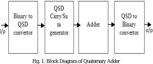
In digital systems like computers and digital signal processors arithmetic operation plays a very important role. Arithmetic operations based on binary number system include problems like higher propagation delay, circuit complexity. When the number of bits increases the hardware also increases which means complexity goes on increasing. According to moor’s law the number of transistors in an integrated circuit has doubled approximately every two years hence in integrated circuits the number of components goes on increasing because of this interconnects increases, nearly 70 percent area of the chip is occupied by interconnections. This problem can be overcome by multiple value logic concepts. The QSD numbers are both positive and negative numbers.The input to the system is binary numbers, the binary to quaternary conversion unit converts binary input to the quaternary and then it proceeds towards the quaternary adder unit. The quaternary adder unit performs the arithmetic operations like carry free addition on the input data. Finally the output of the quaternary adder unit is given to the quaternary to binary conversion unit to convert it back to binary form.
Fig. 1. Block Diagram of Quaternary Adder
3-bit 2’s complement representation is used for QSD numbers. The formula for decimal conversion is given below.
D=∑ i4ieq. (1)
IV.ADDER/SUBTRACTOR DESIGN
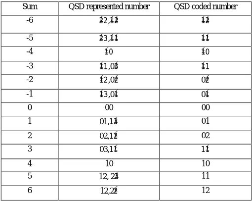
In arithmetic operations adder plays a very important role. To reduce the operation time carry free addition and borrow free subtraction is done. The two steps are available for carry free addition. These two steps involves the generation of intermediate sum and carry and this previously generate intermediate carry is added with current intermediate sum. There are also two rules to avoid carry propagation chain. These two rules says that the sum should not be greater than 2 and carry should not be more than 1 hence by this two rules the addition of second step adder is not greater than 3 and hence it will be single digit QSD number. The range of addition of all combination of addend and augend is from -6 to 6 which are shown in table I.
Table II. Addition of All Combination of Addend and Augend
The above all combinations of addend and augend have the range between -6 to 6. The QSD number representation of this combination is shown in table II. There are multiple representations for these numbers but the numbers which strictly follow the rules are chosen. The representations of the QSD numbers are in a 3 bit 2’s complement binary number. The intermediate carry lies from -1 to 1and because of this it require two bit binary number.
Table II. The QSD Represented and Coded Numbers
Sum QSD represented number QSD coded number
-6 22,12 12
-5 23,11 11
-4 10 10
-3 11,03 11
-2 12,02 02
-1 13,01 01
0 00 00
1 01,13 01
2 02,12 02
3 03,11 11
In the next step the intermediate carry from LSB is added with the sum of the current digit to get the final output because of the previously defined two rules, the next carry is not produce and hence no carry propagation should occurs. The addition in this step has the range from -3 to 3 which is single digit QSD number.
Table III. The Input and Output of Second Step Adder
Input Output
QSD Binary Decimal QSD Binary
Ai Bi Ai Bi Sum Si Si
1 2 01 010 3 3 111
1 1
0 2
01 001
00 010
2 2 2 2 010 010 0 1
1 0
-1 2
00 001
01 000
11 010
1 1 1 1 1 1 001 001 001 0 0
1 -1
-1 1
00 000
01 111
11 001
0 0 0 0 0 0 000 000 000 0 -1
-1 0
1 -2
00 111
11 000
01 110
-1 -1 -1 -1 -1 -1 111 111 111 -1 -1
0 -2
11 111
00 110
-2 -2 -2 -2 110 110
-1 -2 11 110 -3 -3 001
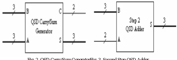
In the first step of addition the QSD carry/sum generator generates the 3 bit sum and the 2 bit carry, this 2 bit generated carry is given to the second step QSD adder which adds the previously generated carry with the current sum and finally the result is obtained. The QSD carry/sum generator and Second step QSD adder is shown in figure 2 and figure 3.
Fig. 2. QSD Carry/Sum GeneratorFig. 3. Second Step QSD Adder
Fig. 4. QSD adder for n number of digits.
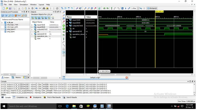
V. SIMULATION RESULTS
The QSD adder programming is written in VHDL and implemented on Spartan 3A (XC3S200A) FPGA board. The simulation is done on Modelsim and the simulation results are shown in the following figures. The figure shows simulation result of quaternary adder.The overall delay of the quaternary adder is total of conversion delay and computation delay.
VI.CONCLUSION AND FUTURE WORK
The quaternary adder is designed and implemented on Spartan 3A FPGA board. The result shows that the performance of quaternary adder is better than binary adder. The quaternary signed digit adder, subtractor is better than any other adder because there is a constant delay which is not depending on number of input bits. Using QSD addition different algorithms for arithmetic operation can be directly implemented. The conversion of binary to quaternary circuit is feasible and efficient in terms of power consumption and speed while being implemented in a standard CMOS technology. As technologies are becoming more complex, multi valued logic (MVL) will be the future of circuit design. Since the research is still in initial stage on MVL the work is fundamental. When hardware implementation using MVL circuits is famous and more exposed to companies then one day MVL will surely turn over the binary logic. The advantages of lower power, higher performance, and reduced interconnect congestion motivate the use of quaternary circuits in a wide variety of applications.
ACKNOWLEDGMENT
Authors would like to express their gratitude towards respected PG coordinator Prof. M.M. Jadhav for his dynamic and valuable guidance and also grateful to him for his constant encouragement in fulfilment of paper. Authors would also like to thank Dr. S.D. Lokhande principal, SCOE Pune, for providing with all necessary infrastructure and facilities to complete the review paper.
REFERENCES
1. DiogoBrito, Jorge Fernandes, Paulo Flores, Jose Monteiro, TaimurRabuske, Senior member IEEE “ Quaternary Logic Look up Table in standard CMOS” 2014 IEEE transaction on very large scale integration system.
2. A.N.Nagamani ,Nischai S. PES institute of Technology, Karnataka, “ Quteranary High Performance Arithmatic Logic Unit Design” 2011 Euromica Conference.
3. SachinDubey, Reena Rani, SarojKumari“ VLSI implementation of Fast Addition using Quaternary Signed Digit Number System” 2013 IEEE International Conference on Emerging Trends in Computing, Communication and Nanotechnology (ICECCN 2013).
4. Marcus Ritt, Carlos Arthur Lang Lisboa, Luigi Carro, Cristiano Lizzari, “A cost effective Technique for mapping BLUTs to QLUTs in FPGAs” 2010 IEEE conference.
5. JeongBeom Kim, Dept. of Elec. Engg. KangwonNatioinal university, Chunchon, south korea,” Area Efficient multiplier using current mode Quaternary logic Technoque” 2010, 10th IEEE conference.
6. O. Ishizuka, A. Ohta, K. Tannno, Z. Tang, D. Handoko, “VLSI design of a quaternary multiplier with direct generation of partial products,” Proceedings of the 27th International Symposium on Multiple-Valued Logic,pp. 169-174, 1997.
7. N. Takagi, H. Yasuura, and S. Yajima, “High Speed VLSI Multiplication Algorithm with a Redundant Binary Addition Tree,” IEEE Trans. Comp., C-34, pp. 789-795, 1985.
8. Steve Hung Lung, “Skew Tolerant Domino Techniques for High speedBough Wooley Multiplier circuit Design”, IEEE Journal on Circuit and systems, Vol 2, pp 424-427.
9. Namba K. and Ito H., Design of defect tolerant s WallaceMultiplier ”, IEEE Symposium on Dependable Computing Vol.2,pp 5-9, Dec2005.
10. M. E. Louie and M. D. Ercegovac,” On Digit –RecurrenceDivision Implementations for Field Programmable gate Arrays” In Proc. Ofthe 11th symposium on Computer Arithmetic, PP. 202-209, Canada.
11. A. Avizienis, “Signed-Digit Number Representation for Fast ParallelArithmetic, ”IRE Transaction Electron. Comp., EC-10, pp. 389-400, 1961.