ABSTRACT
Bhate Kaustubh, Ramesh. Design and Fabrication of a MEMS Pressure Sensor and Developing a Release Protocol for MEMS (Under the guidance of Dr. Paul Franzon and Dr. Christine Grant)
Design and Fabrication of a MEMS Pressure Sensor
and
Developing a Release Protocol for MEMS.
by
Kaustubh Ramesh Bhate
A thesis submitted to the Graduate Faculty of
North Carolina State University
in partial fulfillment of the requirements for the degree in Master of Science in Electrical Engineering.
Department of Electrical and Computer Engineering
Raleigh
2002
Approved by:
Dr Paul D. Franzon Chairman, Advisory Committee
Dr Christine S. Grant Co-chair, Advisory Committee
Biography
Acknowledgements
I am grateful to my advisors Dr. Paul Franzon and Dr. Christine Grant for the opportunity to work in the field of MEMS, which is a fast growing area and for guiding my research through the course of my Master’s Program. Many thanks to my thesis committee member Dr. Griff Bilbro for his encouragement and reviewing my thesis. I would like to thank Dr. Jacqueline Krim for her support during the course of the project. I would also like to thank all my colleagues at Riddick Laboratories as well as at EGRC for making them wonderful places to work in.
Contents
List of Figures vi
List of Tables viii
1 Introduction……….1
1.1Introduction to Micromachined Devices ……….1
1.2Issues in MEMS………3
2 Background and Literature Review………6
2.1Pressure Sensor Designs………...6
2.2 Capacitive Pressure Sensors………8
2.3 Resonant Pressure Sensor………9
2.4Planar Surface Micromachined Pressure Sensor………10
2.5 Piezoresistive Pressure Sensors………..12
3 Piezoresistive Pressure Sensor for the Textile Industry………13
3.1Application of Pressure Sensor………...13
3.2Piezoresistivity………14
3.2.1 Longitudinal and Transverse Piezoresistance………...14
3.2.2 Piezoresistive coefficients of Silicon………15
3.3Resistor Orientation………15
3.4Modeling the Sensor………...17
4 Design, Simulation and Fabrication of the Pressure Sensor……….19
4.1Design of the MEMS Pressure Sensor………19
4.1.1 Mask Layout……….20
4.1.2 Alignment Marks………..22
4.2Simulation of the Pressure Sensor………..22
4.2.1 Process Definition……….22
4.2.2 Generation of 3-D Model………..23
4.2.3 Meshing of the 3-D Model………24
4.3Fabrication of the Pressure Sensor………..25
4.3.1 Choice of Pre-thinned wafers………26
4.3.2 Handling Pre-thinned Wafers………26
4.3.3 Nitride Deposition……….28
4.3.4 LTO Deposition……….29
4.3.5 Photolithography………31
4.3.6 LTO Etch………...31
4.3.7 Strip Photoresist……….32
4.3.8 Nitride Etch………32
4.3.9 Bulk Etch of Silicon………...33
4.3.10 Diffusion………34
4.3.12 Aluminum Deposition and Etching………...35
5 Developing a Release Protocol for MEMS………...36
5.1 Sticking Problems During Release ………37
5.1.1 Stiction………...38
5.2 Stiction Reduction During Wet Release………....38
5.2.1 Vapor Phase Sacrificial Layer Etch………...38
5.2.2 Geometry/Process Specific Release Methods………....39
5.2.3 Supercritical Drying………...40
5.3 Anti Stiction Coatings ………...41
5.4 Release of MEMS Devices Made in SUMMIT Process………42
5.4.1 Release Procedure………..43
5.4.2 Observations………..43
5.4.3 Testing the Released Chips………....44
5.5 Design of Cantilever Beams to Characterize Stiction………....45
5.5.1 Application and Testing of Cantilever Beams………...47
6 Conclusion and Future Work……….50
6.1 Textiles Pressure Sensor………50
6.2 Release Protocol for MEMS Devices………51
Bibliography………..53
Appendix A………55
Appendix B………62
Appendix C………64
Appendix D………65
List of Figures
1.1Layout of the 25 X 25 Array of Pressure Sensor……….……..3
2.1 Pressure Sensor Designs………..7
2.2 Capacitive Membrane Pressure Sensor………..9
2.3 Cross-section of a Resonant Pressure Sensor………...10
2.4 Schematic Fabrication process for nitride diaphragm sensor………11
3.1 Lateral and Transverse Piezoresistor Placements………16
3.2 Layout of the sensor in Cadence-Virtuoso………16
4.1 Masks of the Sensor……….20
4.2 Cross-section of the Pressure Sensor……….21
4.3 Alignment marks ………22
4.4 3-D Model in MEMCAD……….23
4.5 Meshed 3-D Model in MEMCAD……….…..24
4.6 Process flow for the Fabrication of the Pressure Sensor………..25
4.7 Arrangement of Wafers for LPCVD runs……….28
5.1 Illustration of the use of sacrificial layer………...37
5.2 Illustration of different forces during release………..38
5.3 Anti-stiction structure improving release yield………39
5.4 Phase relationships in critical point drying………..40
5.5 Stack-up of layers in SUMMIT……….42
5.6a No stiction after release………45
5.6b Effect of stiction after release………..45
5.7 Projected drying steps for evaporation release of two cantilever beams with different width………...46
5.8 Layout of cantilever beams in Cadence-Virtuoso………48
5.9 Individual beam structures………49
7.2 Result from MEMCAD Simulation showing the Displacement magnitude across the diaphragm………..62 7.3 Observation with water as a rinsing solution after release………...64 7.4 Observation after rinsing the released chip with Methanol………..64
List of Tables
Table 1: Calculation of TMAH etch rate on nitride………56
Table 2: Nitride thickness measurements on first batch of wafers………...57
Table 3: Nitride thickness Measurements on monitor for second batch of wafers..58
Table 4: LTO thickness measurement on first batch of wafers……….58
Table 5: LTO thickness measurements on second batch of wafers………...59
Table 6: Etch rate of “trans-N” on nitride………...59
Table 7: Etch rate of “trans-N” on LTO………..60
Chapter 1
Introduction
1.1 Introduction to Micromachined Devices
The acronym MEMS stands for “Microelectromechanical Systems”. These systems
consist of microfabricated sensors, actuators and other structures that have become increasingly popular in many areas of science and engineering. The field of MEMS has evolved because of the fact that silicon and other semiconductors can be used to fabricate not only integrated electronic circuits, but also transducers and other devices by the use of similar lithographic and other microfabrication techniques. These techniques that are
used to carry out fabrication of MEMS devices are referred to as “micromachining”.
Numerous Micromachined Sensors have been developed so far and this has been possible mainly because of the fact that silicon possesses remarkable mechanical properties. These sensors have a wide range of applications: pressure measurement, optical interconnects in VLSI technology, microfluidic systems, inertial sensing and RF devices. A market study by System Planning Corporation (SPC (1999)) indicates that Pressure Sensors dominate over other MEMS applications [1].
This thesis aims at designing, simulating and fabricating a MEMS Pressure sensor to be used in the Textile Industry. The sensor has been designed for the specific application of measurement of tension in a thread that is being woven around a yarn.
stress in the piezoresistive element changing the value of its original resistance. If the sensor is calibrated then, the stress in the thread can be measured in terms of change of resistance of the piezoresistive element.
The main contribution of this thesis is in the design, simulation and in-house fabrication of the pressure sensor. For static simulation of the device, MEMCAD tool from Microcosm has been used. The design for the pressure sensor starts with a 2D layout in Cadence-Virtuoso, followed by a 3D model in MEMCAD. The tool MEMMech within MEMCAD is used to carry out simulations of the effect of various values of diaphragm thicknesses on the piezoresistive element. This analysis gives an idea of how the actual device will behave after fabrication.
After performing the above simulations, the layout of the sensor array is sent out for making hard masks to be used in fabrication of the device. These masks have been used in the various lithographic steps carried out in the fabrication of the sensors. Pre-thinned 4-inch wafers of (100), p-type silicon have been used for the fabrication of the pressure sensor. These wafers are 100um and 200um thick and polished on both sides. The wafers are bulk etched from one side to create a diaphragm type structure and the piezoresistive element is fabricated on the other side of wafer. The wafers have a 25X25 array of the pressure sensor. Fig 1.1 shows the array of structures on the wafers.
1.1: Layout of the 25 X 25 array of the pressure sensor.
1.2 Issues in MEMS
Currently, three fabrication techniques are used to design MEMS structures viz. Surface micromachining, Bulk micromachining and the LIGA process. In surface micromachining, structures are built on top of the silicon wafer using thin films deposited through various standard methods similar to IC fabrication. Bulk micromachining involves etching away selected portions of the substrate to produce overhanging movable structures on top of silicon wafer. Some of the standardized processes that cater to the fabrication needs of all MEMS devices are MUMPS and SUMMIT. Multi-User MEMS Process (MUMPS) renders cost effective surface micromachining fabrication and is provided by MCNC (Microelectronics Center of North Carolina) in RTP, North Carolina. It is a three-layer polysilicon surface micromachining process involving polysilicon, metal and PSG sacrificial layers. The SUMMIT (Sandia's Ultra-planar Multi-level MEMS Technology) process is provided by Sandia National Laboratories. This is a five-layer surface micromachining process. The LIGA (Lithographic, Galvanoformung, Abformung) is a micromachining process that makes plastic and metal parts with high accuracy.
A well-known problem in the fabrication of MEMS devices from surface micromachining is stiction, which occurs when surface adhesion forces are higher than the mechanical restoring force of the microstructure. When a device is removed from the aqueous solution after wet etching of an underlying sacrificial layer, the liquid meniscus formed on hydrophilic surfaces pulls the microstructure towards the substrate and stiction occurs. A more difficult problem is in-use stiction that occurs during operation when microstructures come into contact.
One attractive approach to tackle the stiction problem is to provide low-energy surface coating in the form of an organic passivation layer on the inorganic surface. Another approach to eliminate in-use stiction is the formation of siloxane self assembled monolayers (SAMs) on the oxide terminated surface.
or self assembled monolayers to eliminate stiction. The main contribution of this thesis has been the use of wet etching techniques for the release of complex MEMS structures made in the SUMMIT process, as so far SUMMIT devices have been released using
supercritical CO2. This release process can be standardized to release other MEMS
devices made in the SUMMIT process.
As a continuing part of this research work, cantilever beams have been designed in the SUMMIT process and sent to Sandia National Laboratories for fabrication. These beams have varying length, width and mass and can be used to detect the presence of stiction during release. These structures can also be used to deposit low-energy surface coatings or self assembled monolayers (SAMs) to study and characterize stiction.
Chapter 2
Background and Literature Survey
In this chapter, a brief review of the existing work and literature in the filed of Pressure sensors is presented.
Pressure sensors represent a fairly mature and commercially viable area for micromachined mechanical sensors. There is an enormous range of applications for sensing pressure in liquids and gases. Examples include automotive manifold air pressure systems, aerospace systems, medical and many other. Micromachining technology has been able to make large inroads into this area due to improved performance, reduced size and reduced cost.
2.1 Pressure Sensor Designs
Most pressure sensor today use sealed gas or vacuum filled cavities. The basic operation of such a sensor is to couple the pressure to be measured to one surface of a membrane and to measure its deflection. To measure the displacement, any suitable sensing technique can be used, including strain gauges, capacitance, piezoelectric, optical and any other.
Fig 2.1 Pressure sensor designs [1]
For a circular clamped membrane, the deflection of the center can be related to pressure by
P*r4 = 16 y 7-v y 3
E*h4 3(1-v2) h 3(1-v) h …………..(2.1)
where,
P = applied pressure, in Pa R = diaphragm radius, in m E = young’s modulus, in Pa h = diaphragm thickness, in m v = Poisson’s ratio
y = deflection at the diaphragm’s center, in m.
2.2 Capacitive Pressure Sensors
Capacitive sensing mechanisms can readily be employed to realize pressure sensors, despite the fact that this mechanism is inherently non-linear (because capacitance is inversely proportional to gap width).
Since the membranes employed are typically clamped at all edges, the capacitance of such membrane structures is not given simply by the parallel-plate capacitor equation, but it can be used as a crude starting point,
C= ∈0*A ……….(2.2)
D
which gives a DC in terms of change in gap width, δd, of,
DC = - ∈0*A*δd ………...(2.3)
d2
An interesting example of a micromachined capacitive pressure sensor is an acutely implantable blood pressure sensor developed at the University of Michigan [3]. They fabricated pressure transducer membranes using boron-selective EDP etching of structures that were anodically bonded to a glass substrate pre-etched to form cavities for lead attachment and metallized to form the lower capacitor plate and interconnections to a separate CMOS processor chip.
nitride electrical insulating layer on the surface of the diaphragm. The silicon wafer was anodically bonded to a metallized glass wafer containing the opposite capacitor plates,
Fig 2.2 Capacitive membrane pressure sensor [3]
bond pads and etched grooves to accept interconnect wires. The silicon wafer was then etched away in EDP, leaving behind the membranes.
2.3 Resonant Pressure Sensor
Resonating structures make use of the fact that measurement of frequency is one of the most robust and high precision methods available, and also that their resonant frequency is generally not a function of the imperfections of electronics.
6um thickness. A passivation layer was then formed on the top wafer and the sensing piezoresistors were formed using ion implantation, after which contact holes for metallization to connect to the diffused deflection electrodes were etched. Bond pads and interconnect metallization were then deposited and patterned, followed by etching of the diaphragm from the back of the wafer. Finally, two slots were etched next to the beam to release it over the buried cavity.
The beam was resonated by applying signals as small as a few millivolts between the beam and the deflection electrode and providing feedback from the piezoresistors in the beam. Pressure applied to the underlying wafer’s diaphragm increases the tension on the resonating beam, increasing its resonant frequency.
Fig 2.3 Cross-section of the resonant pressure sensor [4]
2.4 Planar Surface Micromachined Pressure Sensor
polishing (CMP) process. CMP eliminates many of the fabrication problems associated with photolithography, dry etch, and metallization of nonplanar devices and adds design flexibility.
The fabrication process is shown in Fig. 2.4. In the first step, two separate trenches are etched into the silicon substrate (Fig. 2.4a). The first trench is shallow (0.3um) while the second trench is deeper (2 um). The shallow trench serves as a narrow etch port, which can be easily sealed at a later point in the process. Once the trenches are etched a silicon nitride liner is deposited (0.3um). The trenches are then filled with CVD oxides (Fig. 2.4b). The borophosphosilicate glass is used to shorten the release etch times. For polysilicon diaphragms, 2.4 um oxide film is used. Then, the wafers are polished using a colloidal fumed silica slurry and a polyurethane pad (Fig. 2.3c). Then diaphragm material (low stress silicon nitride or fine-grained polysilicon) is deposited and patterned for etch ports. (Fig. 2.4d). The release etch is than performed and the wafers are rinsed, dried and
sealed. (Fig. 2.4e). The diaphragms are sealed by a 0.3µm low stress nitride deposition.
Since deposition is done in LPCVD system, near vacuum persists in the cavity after sealing and serves as a reference pressure. Processing continues with the deposition and ion implantation of polysilicon piezoresistors. After implant polysilicon is patterned followed by aluminum deposition and pattern (Fig. 2.4f), and the device is ready to be tested.
2.5 Piezoresistive Pressure Sensors
Chapter 3
Piezoresistive Pressure Sensor for the Textile
Industry.
As suggested in the introduction this thesis aims at developing a MEMS pressure sensor
for the specific application in the Textile industry. The choice of the piezoresistive
transducer element is purely guided by the specific application needs. The sensor needs to withstand the pressure that it will measure and at the same time provide an accurate value of the pressure. Also the pressure sensor needed to be fabricated in-house thus limiting the different processing steps that could be performed in the device fabrication.
3.1 Application of the Pressure Sensor
3.2 Piezoresistivity
Piezoresistivity is a widely used physical effect that has its name derived from the Greek word “piezen”, meaning to apply pressure [5]. It is a phenomenon by which an electrical resistance changes in response to mechanical stress.
Piezoresistivity arises from the deformation of the energy bands as a result of applied stress. In turn, the deformed bands affect the effective mass and mobility of electrons and holes, hence modifying resistivity.
3.2.1 Longitudinal and Transverse Piezoresistance
If a relatively long, relatively narrow resistor is defined in a planar structure then the primary current density and electric field are both along the long axis of the resistor. This axis need not coincide with the cubic crystal axes [6]. Therefore it is necessary to know how to transform the peizoresistive equations to an arbitrary coordinate system. The structures are typically designed so that one of the axes of principal in-plane stress is also along the resistor axis. This permits a simplification of the piezoresistive formulation to the form shown in equation 3.1.l
δR/R =πpσp + πtσt …………(3.1)
where R is the resistance of the resistor and the proportionality constants, πp and πt are
called the parallel and perpendicular piezoresistive coefficients, respectively, and are related to the gauge factor by the Young’s modulus of the material.
The general expressions for πp and πt are given by:
πp = π11 – 2 ( π11 - π12 - π44) (l12 m12 + l12 n12 +m12 n12) ………(3.2)
and
where (l1, m1, n1) and (l2,m2,n2) are directional cosines between the longitudinal resistor
direction (subscript 1) and the crystal axis, and between the transverse resistor direction (subscript 2) and the crystal axis. In many silicon micromachined devices, resistors are
oriented along [110] directions in (100) wafers. The longitudinal cosines are (1/√2,
1/√2,0) and the transverse direction cosines are (-1/√2, 1/√2,0). This results in:
πp,110 = ½ (π11 + π12 + π44) ………(3.4)
and
πt,110 = ½ ( π11 + π12 - π44) ………(3.5)
3.2.2 Piezoresistive Coefficients of Silicon
The piezoresistive coefficients are dependent on crystal orientation and can change significantly from one direction to another [6]. They also depend on dopant type (n-type vs. p-type) and concentration. These coefficients are a weak function of doping level for
doping below about 1019 cm-3 but then decrease markedly for high doping. The
coefficients decrease with increasing temperature, dropping to about 0.7 of their room
temperature value at 150°C. The temperature dependence is nonlinear which aggravates
the problem of compensating for temperature dependence. An important fact is that at higher doping levels, the temperature dependence of piezoresistive coefficients becomes small.
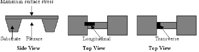
3.3 Resistor Orientation
When the actual size of the resistor is taken into account, the transverse resistor orientation has the potential for the largest response, because if it can be placed at exactly the right point, the entire resistor will experience the maximum bending stress [6]. However, this orientation is very susceptible to manufacturing variations that can arise from small lithographic alignment errors. The longitudinal resistor, on the other hand, must extend over some finite length along the cantilever and, for alignment reasons, may also extend onto the support. Therefore not every part of the resistor experiences the maximum stress, and some loss of sensitivity results. However, small misalignments or placement errors will have a less severe effect than for the transverse orientation. Hence to address these issues a resistor placement is used that is reasonably insensitive to alignment tolerances. The resistor is divided into two sections and spans over the entire area of the diaphragm for maximum sensitivity.
Fig 3.2 Layout of the sensor in Cadence-Virtuoso
The structure shown in the above figure is bulk micromachined and hence all resistor axes are along the <110> directions and are aligned along an axis of principal stress at the edge of the plate. Further, as these resistors are on a plate rather than a cantilever, each resistor experiences both a longitudinal stress and transverse stress. For example, if the resistor R1 experiences a longitudinal stress σl, then it must simultaneously experience a
transverse stress νσt , where ν is the Poisson’s ratio. Otherwise it would shrink in the
transverse direction, which is not allowed in a plate. As a result, the total change in resistance for R1, assuming uniform stress over the entire resistor would be
δR1/R1= (πl + νπl) σl …………(3.6)
The Poisson ratio happens to have a minimum in the [110] direction of a (100) plane,
with a value of 0.064. Assuming resistor orientation along [110] direction, πl for a n-type
piezoresistor is –31.2*10-11 Pa and equation 3.6 becomes
δR1/R1= (-33.19*10-11) σl …………(3.7)
3.4 Modeling the Sensor
The diaphragm is modeled as a square plate under stress. An energy-method analysis [6] gives the load-deflection equation of the form
P =
{
Cr[σ0*H/L2] + Cb[E*H3/(1-ν2)*L4]}
c1 + Cs*ƒs[E*H/(1-ν)*L4]c13 ……(3.8)where Cr is the coefficient of the residual stress term, Cb is the coefficient of the plate
bending term, and Cs is the coefficient of the large-amplitude-in-plane stretching term.
amplitude loading Cs is ignored. The value of Cb from variational analysis is π4/6. Thus
the energy method solution has pressure-deflection relation
P = [π4/6*(E* H3)* c
1]/(1-ν2)*L4 ………..(3.9)
where L = edge length of the diaphragm, c1 = displacement at the center of the
diaphragm, E = Young’s Modulus, H = the diaphragm thickness and ν = Poisson’s ratio.
The magnitude of the x-directed surface stress at the middle of the diaphragm edge is
σx = E*H/ 2ρx …………(3.10)
where the x-directed radius of curvature is given by
1/ρx = (2π/L)2 *c1/2 ………..(3.11)
Thus σx can be expressed as
σx = 1/π2(1-ν2)*(L/H)2 * P ……….(3.12)
and because we are dealing with a plate, the y-directed stress at the center of the edge is
σy = νσx …………(3.13)
Chapter 4
Design, Simulation and Fabrication of the
Pressure sensor.
As mentioned in the introduction, this thesis aims at developing a pressure sensor that can be used in the Textile industry to measure the stress in the yarn while it is being woven. This chapter discusses the various issues faced during the different stages of the making of this sensor. This chapter will give an overview of the design of the pressure sensor, its simulation using the software tool MEMCAD and finally the various issues faced while attempting the fabrication of the pressure sensor.
4.1 Design of the MEMS Pressure Sensor
4.1.1 Mask Layout
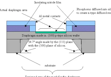
The current design for MEMS starts from drawing the mask layout of different layers involved in the fabrication process by using a layout editor. This procedure is the same as generating the layout of a VLSI circuit. Cadence Virtuoso layout editor was used for this purpose. The mask layout information was drawn by this layout editor. It saves the MEMS structures in CIF (Caltech Interchange format) or GDS-II format which is then sent over for fabrication. Since the sensor was going to be fabricated in-house no particular design rules were considered. The layout of the pressure sensor is shown in the Fig. 4.1 [7].
Fig 4.1 Masks of the sensor
of the mask that was designed for it as can be seen from the Fig.4.2.
Fig 4.2 Cross-section of the pressure sensor.
4.1.2 Alignment Marks
Fig 4.3 Alignment marks on the masks
The alignment marks shown in Fig 4.3 are designed to align the METAL1 layer to the HOLE2 layer during lithography. These alignment marks are placed on either side of the 25 X 25 array of sensors to minimize alignment errors.
4.2 Simulation of the Pressure Sensor
4.2.1 Process Definition
depending upon how the etch masks have been defined. Modeling the process steps by MEMCAD involves specifying a series of deposit and etch steps depending on the fabrication process. It describes the type of deposited film and it’s thickness, the name of the mask from the layout editor used to etch off the layer and also the angle and offset which can be specified to take care of fabrication faults.
The nitride film deposited on the wafer is described as planar. The masks P1P2VIA and HOLE2 are described as having negative polarities as they are used to etch away the nitride layer on the frontside and the backside of the wafer respectively. The METAL1 mask is defined as positive as it indicates areas on the wafers where metal should remain.
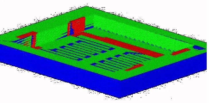
4.2.2 Generation of 3D Model
From the 2D-mask layout information and the elevation information from the process definition, a 3D model of the MEMS structure is generated. The generated CIF file of the layout is first exported from Cadence Virtuoso and then imported by the layout editor Catapult in MEMCAD. MEMCAD uses a 3D-model generator from SDRC, “I-DEAS” to do it. The 3D model generator builds up the model in steps, by getting the height and depth information from the process file, at every deposit and etch step, along with the 2D geometry of the concerned mask layer from the CIF file. The 3D model generated by MEMCAD is shown in Fig 4.4.
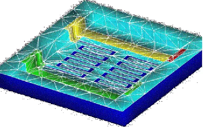
4.2.3 Meshing of the 3D model
Complicated geometries arise in various applications like thermodynamics, structural analysis, electromagnetics and acoustics. In each of these areas, a partial differentiation equation or a series of partial differential equations are needed to be solved on a geometric region. A method of choice here is finite element analysis, which has meshing as the first step of operation. Meshing or mesh generation involves breaking down the solid structure into small subparts, and the differential equations are solved on each subpart [8]. The meshes created have a tremendous impact on the solution of the numerical model; both with respect to accuracy and the extent of computational resources they demand. To get the best possible solution while still maintaining minimum computational leads, the following criterion should be met:
• Keep the number of nodes to a minimum to save computational resources.
• Have sufficient number of nodes especially on the corners where high gradients of the
function solved are encountered, where the domain boundaries need to be specified in detail.
The final meshed structure for the Pressure Sensor is shown in Fig 4.5.
4.3 Fabrication of the Pressure Sensor
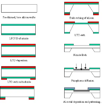
The Fig. 4.6 shows a bird’s eye view of the process flow for the pressure sensor.
Fig 4.6 Process flow for the fabrication of the pressure sensor.
includes the documentation of the different process conditions for the various processing steps that will be carried out.
4.3.1 Choice of Pre-thinned wafers
Based on the design of the process flow for the sensor it is clear that the wafers, on which the device will be fabricated, will need to be bulk etched. There are two types of chemicals to do bulk etching of silicon viz. isotropic etchants and anisotropic etchants. Isotropic etchants like HNA (mixture of hydrofluoric acid, nitric acid and acetic acid) will etch silicon at the same rate in all the directions whereas anisotropic etchants like TMAH (tetramethyl ammonium hydroxide) and KOH (potassium hydroxide) etch silicon much faster in the (100) direction than in the (111) direction. Based on the geometry of the structure that is required to create the diaphragm it was decided to use an anisotropic etchant to do the bulk etch of silicon.
Potassium being a contaminant for CMOS processes, KOH cannot be used in the cleanroom to etch silicon and hence TMAH was the likely choice. Literature predicts that the most optimistic etch-rate of silicon by TMAH is 1um/min which means that in order
to etch a regular 500+/-25 um thick wafer to create a diaphragm of 20µm, the etch time
would be around 500 minutes (more than 8 hours of continuous etch). This is very difficult to achieve with a continuous uniform etch rate and hence it was decided that in order to reduce the etch time of silicon and maintain a uniformity in the etch rate,
pre-thinned wafers would be used. These wafers are available in 100 µm and 200 µm
thicknesses and would take a maximum of about 3 hours of bulk-etch time based on the literature data available.
4.3.2 Handling Pre-thinned wafers
wet etch boats. Both surfaces of these wafers are polished and it is not possible to write a name on these wafers using a scribe. These wafers cannot be dried using the regular spin dryer, as there is every possibility that they may break during this operation. Hence they need to be dried by a nitrogen gun (blow dryer) which also again needs to be done very carefully. Wet chemical processing is especially difficult because when picking up the wet wafers by a tweezer, the surface tension of the water between the wafer-tweezer contact causes the wafer to stick to the tweezer and it becomes extremely difficult to get the wafer off the tweezer without breaking it. The vacuum-operated holder also cannot be used to pick the wafers because the vacuum sucks the thin wafer at the contact, causing a pit to appear on the other side.
In order to make the wafers more robust in handling, during some of the processing steps, it was decided to bond a thin wafer to a normal substrate by means of glue. To serve this
purpose, CrystalbondTM 509 (glue) is used. It comes in the form of small candle-size
sticks and is very easy to use [9].
The substrate wafer is placed on a hot plate and heated to about 110° C. The glue-stick is then moved along the edge of this wafer, causing the glue to melt on the surface of the wafer. The hot plate is then turned off and the wafer is allowed to cool to room temperature. The thin wafer is then placed on top of this substrate-wafer that has solidified glue on it. The thin wafer is aligned so that it is exactly on top of the substrate and then the hot plate is turned on again with the set point at 110° C. At this temperature the glue sandwiched between the two wafers melts again and serves to bond the two wafers together. This sandwiched assembly can then be used directly for processing in certain process steps like spinning photoresist (PR) and wet etching.
and cleans the wafers, which can then even be put in the furnace to do any other processing step.
4.3.3 Nitride deposition
A nitride film is deposited on the silicon wafers to act as an insulating layer. Silicon nitride is highly suitable for this purpose because it behaves as a nearly impervious barrier to diffusion [10]. The film is deposited by a method called Low Pressure Chemical Vapor Deposition (LPCVD). Since this process is carried out in very low pressures it is surface reaction limited and the transportation of chemicals is not important allowing the wafers to be stacked in the furnace. The method also provides a higher throughput if the temperatures are lowered. However as the temperature is lowered, the deposition rate can decrease significantly and the film quality may suffer.
Fig 4.7 Arrangement of wafers for LPCVD runs [10]
The nitride film was deposited at temperatures of 800°C, 775°C, 775°C for the front,
opposite directions. A monitor wafer is put in the furnace in the middle of the thin wafers so that the measurements (Table 2 and Table 3 in Appendix) of the monitor are an average indication of the film thickness on the first and the last pre-thinned wafer in the stack.
After the nitride film has been deposited, its’ thickness is measured using Ellipsometry at different points on the wafer. From these results the average film thickness and the deposition rate of nitride is calculated.
This deposited nitride film will act as a mask to protect the rest of the silicon wafer when it’s desired part is being bulk etched in TMAH. This film also serves as a mask to prevent the diffusion of phosphorus atoms into the silicon wafers in areas other than where the piezoresistors have been defined. A wafer with known nitride film thickness is put in
TMAH solution at 90°C and a procedure identical to that used in bulk etching silicon is
followed. The wafer is etched for 50 minutes and then the nitride film thickness is measured again (Table 1 in Appendix). It is found that the nitride film is almost untouched by the TMAH solution, thus proving that it is the right choice as a mask for the wafer.
4.3.4 LTO Deposition
When non-plasma silane deposition of oxygen is done at temperature less than 500°C, it
The purpose of the LTO film here is to act as a mask to protect the nitride film from being etched away except from the area where the piezoresistors are fabricated. Nitride film is etched in a solution called the trans-N etch at 180°C. To calculate the desired LTO film thickness on nitride, the etch rate of trans-N on LTO is calculated. A dummy wafer with known LTO film thickness on it, is put in the etch solution for 8 minutes and then the film thickness is measured again using Ellipsometer. It is observed that the etch rate of trans-N on LTO is about 30A°/min at 180°C (Table 7 in Appendix). Similarly, the etch rate of trans-N on nitride is calculated and from the data now available the thickness of the LTO film to be deposited on nitride is obtained.
For LTO deposition the wafers are loaded with their major flats at the top. A bare silicon monitor wafer is also included in the stack of wafers because LTO thickness on nitride cannot be measured. The monitor wafer is placed in the middle of the thin wafers so that its thickness is the average thickness of LTO on the first and the last of the wafers. The slot numbers of the boat, in which the wafers are loaded, are also noted. The LTO deposition is carried out at about 410°C with pressure of 660 mTorr. The gas flow of the gases in the furnace is also noted.
4.3.5 Photolithography
After LTO depositions the wafers are taken for lithography. The photoresist Shipley1813 is spun on the wafers at 4000 rpm for 40 seconds. The Shipley1813 is a positive photoresist i.e. the photoresist will dissolve in the developer solution wherever it has been exposed. Before spinning the PR the wafers are coated with a primer that provides a better contact between the PR and the wafer.
After spinning PR on the wafers they are then exposed to UV light through the mask under consideration (P1P2VIA, HOLE2 and/or METAL1). The expose time is set to 8 seconds.
The wafers are then developed in the Developer solution by immersing them in its bath. The develop time varies from 1.5 to 2 minutes. The wafer-boat is continuously pulled out of the bath to see if the features are visible. Once the features can be seen, the wafers are developed for a few more seconds and then pulled out.
After developing the wafers, they are then hard baked for 1 minute. This hardens the resist and improves it’s ability to act as an etch mask. The photoresist is then used as a mask to etch away the LTO in HF bath.
4.3.6 LTO Etch
LTO is etched away in a solution called “Buffered oxide etch” (BOE) which contains HF. Because LTO is porous and has a lesser density as compared to thermally grown oxide it’s etch rate in HF is much faster (about 1800A°/min) than that of the latter. During the etch step a monitor wafer is also put in the BOE bath to help determine the endpoint of the etch.
longer clings to the wafer and the wafer become “de-wet”. Once the monitor wafer become “de-wet”, an overetch is done for about 5 sec and the boat is then removed from the solution.
4.3.7 Strip Photoresist
The photoresist is removed by putting the wafers in a solution called Nanostrip. Nanostrip consists of sulfuric acid that dissolves the photoresist on the wafers. The wafers are kept in the “Nanostrip” bath for as long as all the photoresist is not removed. The end point is indicated by clear solution dripping from the wafers when pulled out of the bath rather than dark thick liquid containing photoresist. Sulfuric acid does not affect silicon wafers so the time for which the wafers are kept in the “Nanostrip” bath is not critical. In general it takes about ten minutes to completely strip the photoresist of the wafers.
4.3.8 Nitride Etch
Nitride is etched using a solution called “trans-N” that contains phosphoric acid. The
reaction is carried out at 180°C. The LTO layer serves as a mask for the nitride etch.
From the available data the etch rate of LTO by “trans-N” is about 30A°/min, while that
for nitride varies with the number of wafers in the bath. It is 68A°/min with one wafer in
the bath and drops to about 62A°/min with four wafers in the bath. This is attributed to
the fact that the solution in-between the wafers does not have a continuos circulation and so after sometime the etch rate begins to fall which is ultimately evident in the form of a decrease in the overall etch rate over the period of time.
4.3.9 Bulk Etch of Silicon
Silicon is bulk etched using TMAH (tetramethyl ammonium hydroxide). The reaction is
carrried out by heating the TMAH solution in a petridish, on a hot plate to about 91°C,
and then putting one wafer into it [11].
TMAH is present in all cleanrooms since it is used in developing positive photoresists. A potential trade-off with use of TMAH is that the surface morphology tends to be rough.
An elaborate procedure has been developed to carry out this bulk etch step in order to achieve a uniform etch rate. A known quantity of TMAH is begun to heat. As the TMAH temperature rises it begins to evaporate and the quantity of the solution in the dish begins to change. To prevent this the dish is covered when being heated to minimize the evaporation. The temperature of the TMAH solution is indicated by using a thermocouple. The etch rate of silicon depends on the temperature as well as the volume of the TMAH in the dish and hence these two parameters need to be controlled as accurately as possible. To reduce the effects of TMAH evaporation the solution in the dish is replenished from time to time to keep the volume of the solution in the dish a
constant. When the solution temperature reaches 91°C, a wafer is put in the dish to start the bulk etching.
Silicon begins to get etched where it is exposed. As more and more silicon is etched, the concentration of silicon in the TMAH solution and the rate of TMAH evaporation also increases, reducing the etch rate. To minimize these effect, the dish is kept covered throughout the etch period and the solution in the dish is replenished frequently.
Literature [11] predicts an etch rate of 1um/min for silicon by TMAH. However the initial obtained etch rate is much less than that. The measurements indicate that the etch
rate is about 0.3µm/min. Also it is observed that for long etch time (more than 30
In order to get a better etch rate, the wafer is glued to another wafer that is coated with a
thick (>2000A°) nitride film, which acts as an excellent mask to protect silicon from
being etched. As a result of this, now only one face of the wafer is exposed to TMAH
during the entire etch cycle. Using this method, an etch rate as high as 43 µm/hr was
obtained, following the same procedure as before.
4.3.10 Diffusion
Phosphorus was diffused into the p-type wafers to create diffused resistors in the wafers. Phosphorus was chosen as the dopant, instead of Boron, because the wafers being p-type and phosphorus being a n-type impurity, there is an isolation between the two.
The wafers were diffused with Phosphorus using phosphorus-disks. The diffusion was
carried out for 70 minutes at 950°C. This long time and high temperature is because of
the fact that the resistance of the piezoresistor need to be reasonably small, below I KΩ. Phosphorus pentoxide is formed on the wafer surface (Table 8 in Appendix), from which the phosphorus then diffuses, into the wafer. The wafers are placed in the following order in the furnace: p-disk, wafer, wafer, p-disk. The wafer pair is placed back-to-back, to prevent the back-side doping of the wafers.
A bare silicon monitor wafer was also put in the furnace to measure the sheet resistance of the wafer after diffusion. Measurements indicate that the sheet resistance in 5.78Ω/ , while the oxide thickness measurements are indicated in Table 8 in the Appendix. Both the measurement results are in accordance with the calibration data sheet of the phosphorus-disks [12].
4.3.11 P-Deglaze
ratio of BOE and water is 1:4. This diluted solution is used to etch the oxide because the
P2O5 glass is easy to etch. The “de-wetting” of the monitor wafer was used as an
end-point in determining the complete removal of the oxide. The recommended time is 30 seconds but the wafers were etched for 40 seconds to make sure that the oxide had been etched from all the wafers, completely.
4.3.12 Aluminum Deposition and Etching
Aluminum was deposited to make contact with the diffused resistors. The metal pads can be used to probe the structure when the fabrication is complete. The metal thickness is chosen to be 2000 A°.
After metal deposition, it was patterned using the METAL1 mask and then the wafers were etched to remove unwanted Aluminum. The aluminum etch is done in a solution composed of: phosphoric acid (80%), nitric acid (5%), C2H4O2 (5%) and distilled water.
Chapter 5
Developing a Release Protocol for MEMS Devices
There have been many exciting predictions that the future of micromachines or MEMS is just “around the corner”, but this future has proven to be slow in coming. Despite the demonstration of numerous MEMS devices and product concepts (Analog Devices, ADXL-50, Capacitive Accelerometer) each year, a very small number have actually succeeded in the market. The most critical impediment to the fabrication and operation of many MEMS devices has been the difficulty in controlling surface forces during processing and operation.
Fig. 5.1 Illustration of the use of sacrificial layer [1]
5.1 Sticking Problems during Wet Release
Attractive capillary forces can be a real problem with wet released microstructures because the drying fluid tends to pull deformable microstructures into contact with the substrate and/or each other. Once deflected, van der Waals forces are responsible for stiction of hydrophobic surfaces and hydrogen bonding is the dominant adhesion mechanism for hydrophilic surfaces [13]. Thus the total forces acting on a structure during release can be summed as
Utotal= Ubending+Ustretching+Usurface tension ……….(5.1)
Fig. 5.2 Illustration of different forces during release [1]
5.1.1 Stiction
A well-known problem in the fabrication of MEMS devices from surface micromachining is stiction. Stiction occurs when surface adhesion forces are higher than the mechanical restoring force for the microstructure. When a device is removed from the aqueous solution after wet etching of an underlying sacrificial layer, the liquid meniscus formed on hydrophilic surface pulls the microstructure towards the substrate and stiction occurs.
5.2 Stiction Reduction during Release
A wide variety of stiction-minimizing process approaches have been developed for surface micromachining applications some of which are described in this section.
.
5.2.1 Vapor-phase Sacrificial Layer Etch
etching the sacrificial silicon dioxide with hydrofluoric acid vapor instead of conventional aqueous HF solution, the need for subsequent rinsing and elaborate drying procedure is eliminated [14]. Condensation of water on the etch surfaces can prevent the success of HF vapor release but the use of anhydrous HF gas and methanol mixture under low pressures solves this problem.
Using this method etch rates of 10 to 15 µm/hr on silicon dioxide for partial pressures of 15 and 4.5 torr for HF and methanol, respectively, were obtained.
However the disadvantage of this method is that, etching in vapor phase is much slower than that in aqueous solution. The speed of etching is a concern when the width of the microstructures is large and when more layers of sacrificial oxide are involved.
5.2.2 Geometry/Process Specific Release Methods
A less general approach to reducing sticking following wet etch release is the use of methods specific to given geometries or processes. Abe, et al [15], studied the drying of post release singly and doubly clamped beams. For singly clamped cantilevers, they observed that for the shorter structures, drying occurred from tip uniformly back to the base, while for longer cantilevers, the fluid dried in the opposite direction, causing stiction problems. By adding small, narrower width protrusions, from the ends of the long cantilevers, sticking was considerably reduced.
5.2.3 Supercritical Drying
The most common method of preventing stiction in MEMS devices during their release is supercritical drying.
Supercritical fluids are compounds heated and pressurized above their critical pressure and temperature, at which point liquid and vapor states become indistinguishable and become a fourth, supercritical state. Supercritical fluid has the attractive property of absence of surface tension due to the coexistence of liquid and vapor states [16].
The basic idea is to take advantage of the fact that, under the correct i.e. (supercritical) conditions, the liquid and vapor phases cease to exist as distinct states as indicated in Fig 5.4. When this occurs the interface between them is eliminated and, after transitioning directly to the gas phase, the gas can be gently vented without disturbing the structures.
A possible choice for use in micromachining is water because it is used in rinsing.
However the critical point for water is 228.5 bar and 374°C that would normally destroy
the substrate. Another possible choice is methanol but this also has high critical point as
well (240°C, 79.9 bar). A material with low critical pressure and temperature is carbon
dioxide (31°C, 73.8 bar), but it is only a liquid at pressures greater than 900 psi. However methanol is completely miscible with liquid carbon dioxide and this provides a good method for using carbon dioxide as drying fluid. Liquid carbon dioxide is used to replace liquid methanol at room temperature and elevated pressure, and then the supercritical transition of carbon dioxide is used to dry the devices.
The Critical Point Drying method is expensive because it requires the use of Critical Point Dryers that have a very high cost. Their cost varies from 8000$ to 13,500$ [17] depending on the manufacturer and the different features available in a particular model. Also, these machines have to be used carefully with proper safety measures because of the high pressures involved.
5.3 Anti-Stiction Coatings
A part of this thesis aims at developing a release protocol for MEMS devices made in the
SUMMITTM process which can then be treated with organic monolayers to eliminate
release-related stiction. SUMMIT devices are normally released using the Supercritical
CO2 drying but this thesis attempts to show that they can be released using a wet etch
step in HF followed by a rinse in methanol. The resulting devices are shown (Appendix C) to be released completely with the total removal of the sacrificial oxide layer. This protocol can be used for the release of any MEMS device made in the SUMMIT process. Once this part of the release process has been standardized, the surface-active agents selected for surface modification can be studied for their effect on release-related stiction.
5.4 Release of MEMS Devices Made in SUMMIT Process
Fig. 5.5 Stack-up of layers in SUMMIT [19].
The Fig 5.5 shows the stack-up of the different layers involved in the SUMMIT process [19]. It can be seen that there are four layers of sacrificial oxide sandwiched between five layers of poylisilicon. Because of this nine layer stackup (as compared to the three polysilicon and two oxide layers resulting in a total of five layers involved in the
MUMPSTM process of Cronos, Inc,) the rate at which the sacrificial oxide can be etched
resulting reduction in the HF solution in contact with the oxide, requires longer release times.
5.4.1 Release Procedure
Literature [20] tells us that in order to release a MEMS device made in the MUMPSTM
process, it is etched in 49% HF for 2.5 minutes, before introducing the sample in DI water for rinsing.
In order to release a chip made in the SUMMIT process we have modified the above recommendation because of the difference in the two fabrication processes. The chip is first put in a 49% HF solution for fifteen minutes. Small fragments are seen being released from the chip, while it is in HF. This is attributed to the fact that HF attacks the oxide present on the chip causing it to dissolve. In addition to this, as HF etches the sacrificial oxide layer, micro-bubbles are observed on the chip surface, indicating a reaction. Following this step, the chip is rinsed with methanol in three steps, each time immersing the chip in fresh methanol solution for ten minutes. The chip has to be handled carefully when moving from one solution to another, in order to avoid mechanical damage to the chip. Also, the transfer from one solution to another should be aimed at minimizing the exposure of the chip to atmosphere. The sample is then placed on a hot
plate at 115°C for approximately 20 minutes. The resulting sample is then taken for
observation under an optical microscope to study the results of the reaction.
5.4.2 Observations
deep inside the chip take a longer time to be etched away and the oxide if present, can be seen under the optical microscope.
In general, after MEMS devices are released, a few of the structures can be seen to be floating on the chip (Appendix C). These are structures that have been completely freed because of an overetch of the underlying sacrificial oxide layer. This was used as a guideline while observing the released chips under the optical microscope, to determine whether the chip was being released.
DI water, instead of methanol, was also initially used to rinse the chips after the HF etch, but the results were not satisfactory. The DI water leaves behind a stain/residue on the chip that can be seen under the optical microscope (Appendix C). As a result, it is difficult to tell whether the chip has been released completely under the stain because looking for oxide on the chip becomes difficult.
5.4.3 Testing the Released Chips
5.5 Design of Cantilever Beams to Characterize Stiction
Cantilever beams are the simplest of all MEMS strutures for design, fabrication as well as testing. Their layout is very easy to design and the calculations involved in the analysis and testing of these structures are also not complex.
If sticking forces present during release are more than the opposing forces (elastic energy stored in the beam, applied voltage to the beam), they pull the beam down towards the substrate. This can be detected very easily by simple observation under an optical microscope. The pulled down portion of the beam appears of a different color than the portion of the beam near the clamp because of difference in the topography. The effect of stiction on a cantilever beam during release is indicated in Fig 5.6a and Fig. 5.6b.
tendency of the drop to be circular (to minimize the free surface area), the final liquid area should be proportional to approximately square of the beam width if the gap is much smaller than the beam width
The cantilever beam will spring back and become a free standing structure i.e. (released) if the elastic energy stored in the pull-down beam is larger than the capillary pull-down energy. For a given beam length, elastic energy is proportional to beam width [21]:
F=ky=w*h3*E*y ………..(5.2) 4*l3
where w= beam-width, h =beam thickness, E = Young’s modulus, y = vertical displacement at the end and l = length. The capillary pull-down energy that causes surface contact is proportional to the square of the width as explained above [20]. Thus the liquid pull-down energy increases at a greater rate than beam elastic energy as width increases and so the maximum detachment length for evaporation drying decreases with increasing width.
Fig. 5.7 Projected drying steps for evaporation release of two cantilever beams with different width [21].
5.5.1 Application and Testing of the Cantilever Beams.
The Fig. 5.8 shows the CAD plot of an array of cantilever beams that have been designed in the SUMMIT process to help in our studies related to stiction. These beams can be used to study release related stiction as well as in-use stiction. These beams can also be probed and tested if required. The probe station, here at NCSU-EGRC-301, can be used for this purpose. Small microprobes hooked onto an oscilloscope and function generator can be used to excite the beams and observe their deflection. Using the microprobes, DC voltage as well as an AC signal can be applied to the beams and their resultant behavior can be studied under the optical microscope.
The beams have been design based on the aforementioned relations between the beam length, beam width and stiction. An array of beams has been created with varying lengths
and widths (lengths varying from 150µm to 500µm and widths varying from 3µm to
50µm). Also, the beams have been made in different polysilicon layers to study the effect of the mass of the beam on release-related stiction.
These structures have been sent to Sandia National Laboratories for fabrication and, are expected to be back by September/October. These beams can be used to study their behavior during the release process and also study the effects of release-related stiction with the varying beam dimensions.
microprobe. The beam support (Fig. 5.9) has been made sufficiently large (40µm X 40µm) to act as a probe pad.
Fig.5.8 Layout of cantilever beams in Cadence-Virtuoso
Chapter 6
Conclusion and Future Work
6.1 Textiles Pressure Sensor
In this thesis an approach has been made in the design and fabrication of a Piezoresistive Pressure Sensor that can be used in Textile Industry. The designed sensor was simulated and analyzed in MEMCAD and then it was attempted to fabricate in the cleanroom at NC State University.
A process flow was designed for fabricating the sensor and a Traveler document was generated in this regard. During the course of Processing it has been found that the chief hurdle in the completion of the sensor fabrication is the “Back-side alignment”. As, in case of many MEMS devices, the fabrication of this Pressure Sensor involves processing of the wafer on both sides. There is front-side processing that involves the fabrication of diffused resistors to act as piezoresistive elements and the back-side processing that involves Bulk etching of the wafer to create a diaphragm underneath the resistors. The Karl Suss MA6 aligner, in the NC State Cleanroom, does not have the provision to do backside alignment and hence the issue arises.
Another approach is to use “through wafer via holes”. By etching via holes in the wafer through the entire wafer, the alignment marks on the mask may then be used as reference to do the front and backside alignment. However this approach is tricky because handling pre-thinned wafers will become very difficult once they have etch holes in them all the way through and hence should be used with caution.
During the fabrication process it is found that, creating an array of diaphragms of 20 um thickness on pre-thinned wafers is very difficult using wet etch techniques like TMAH. The diaphragm breaks either when the wafer is being pulled out of the viscous TMAH solution because of the surface tension of the liquid or when the wafer is being
blow-dried by a nitrogen-gun. Although, etch depths upto 80 µm have been measured, on a 200
µm thick wafer, using the Profilometer, further measurements have not been possible as
the diaphragm breaks down. This problem can be solved by doing a partial wet etch initially as it is faster, and then doing a (dry etch) Reactive Ion Etch (RIE).
Future work will involve working on the backside alignment problem and testing the final pressure sensor device. Once the backside alignment issue is tackled, it will be possible to do the bulk etching step as the last in the fabrication process flow and this will also reduce the handling issues of the pre-thinned wafers post “bulk-etching”.
6.2 Release Protocol for MEMS Devices
A part of this thesis aims at developing a Release Protocol for MEMS devices made in
the SUMMITTM Process. The procedure involves a wet HF etch of the chips made in
SUMMITTM process, followed by drying them and observing and testing them to confirm
that the devices on the chip have been released.
design flaw, in that, the POLY 3 and POLY2 layers were not connected together by means of via holes. Hence the devices could not be tested for their motion by electrical actuation. Further, these devices are RF components like transmission lines and RF switches, which have their own testing issues, and do not have a significant lateral or vertical movement that can indicate that the devices have been released, upon electrical activation.
To circumvent this problem, cantilever beams have been designed in the SUMMITTM
process, and sent to Sandia National Labs for fabrication. Upon, their arrival these devices can be released using the same protocol as above and then electrically tested to observe their motion and confirm the release. Testing of cantilever beams is fairly simple. The entire array of beams has a ground plane, which can be hooked up, as circuit ground. The beam supports (clamps) have been designed to be sufficiently large so as to serve as a landing pad for a test probe or to wire-bond it onto a chip. On applying a suitable activation voltage to the beam and grounding the ground plane, the beam will be attracted towards the substrate and will bend downwards. This motion will vary from 2 um to 10.25 um depending on whether the beam is made of POLY1 or POLY4 layers respectively.
References
[1] “Micromachined Transducers Sourcebook”, Gregory T.A. Kovacs.
[2] Bryzek, J., Petersen, K., Mallon, J. R., Christel, L., and Pourahmadi, F., “Silicon Sensors and Microstructures,” Lucas Novasensor, 1055 Mission Court, Fremont, CA, 1991.
[3] Chao, H.L., and Wise, K.D., “An Ultraminiature Solid – State Pressure Sensor for a Cardiovascular Catheter”, IEEE Transactions on electronic Devices, vol. 35, no. 2, Dec 1988, pp. 2355-2362.
[4] Petersen, K. E., Pourahamdi, F., Brown, J., Parsons, P., Skinner, M., and Tudor, J., “Resonant Beam Pressure Sensor Fabricated with silicon Fusion Bonding”, Proceedings of Transducers’ 91, the 1991 International Conference on Solid-State Sensors and Actuators, San Francisco, CA, June 24 – 27, 1991, pp. 177 – 180.
[5] “An Introduction to Microelectromechanical Systems Engineering”, Nadim Maluf [6] “Microsystem Design”, Stephen D Senturia
[7] Guckel, H., “Surface Micromachined Pressure Transducers,” Sensors and Actuators, vol. A28, no.2, July 1991, pp. 156 – 160.
[8] MEMCAD 3.1 Reference Manual, Microcosm Technologies Inc, Cambridge, MA. [9] Aremco Reference Manual, Aremco Products Inc, NY.
[10] “Silicon VLSI Technology Fundamentals, Practice and Modeling”, James D. Plummer, Michael D. Deal and Peter B. Griffin.
[11] Sato, K., Shikida, M., Yamashiro, T., Asaumi, K., Iriye, Y., and Yamamoto, M. “Anisotropic Etching Rates of Single Crystal Silicon for TMAH Water Solution as a Function Crystallographic Orientation”, Micro Electro Mechanical Systems, 1998. MEMS 1998. Proceedings, The Eleventh Annual International Workshop, 1998, pp. 556-561
[13] Legtenberg, R., Elders, J., and Elwenspoek, M., “Stiction of Surface Microstructures after Rinsing and Drying: Model and Investigation of Adhesion Mechanisms,”
Proceedings of Transducers’93, the 7th International Conference on Solid State Sensors
and Actuators, Yokohama, Japan, June 7 –10, 1993, Institute of Electrical Engineers, Japan, pp. 198-201.
[14] Yong-II, Lee, Kyung-Ho Park, Jonghyun Lee, Chun-Su Lee, Hung Joun Yoo, Chang-Jin Kim, “Dry Release for Surface Micromachining with HF Vapor-Phase Etching,” Journal of Microelectromechanical Systems, vol. 6, no. 3, September 1997. [15] Abe, T., Messner, W. C., and Reed, M. l., “ Effective Methods to Prevent Stiction During Post-Release-Etch Processing,” Proceedings of IEEE Micro Electro Mechanical systems Conference, Amsterdam, Netherlands, Jan 29 – Feb 2, 1995, pp94-99.
[16] Mulhern, G. T., Soane, D. S., and Howe, R. T., “Supercritical Carbon dioxide
Drying of Microstructures,” Proceedings of Transducers’93, the 7th International
Conference on Solid State Sensors and Actuators, Yokohama, Japan, June 7 –10, 1993, Institute of Electrical Engineers, Japan, pp. 269-299.
[17] www.tousimis.com/critical_point_dryers/ MEMS_drying_system.html [18] www.memsurface.com/stiction.html
[19] http://www.sandia.gov/mems/micromachine/5level.html
[20] Kim, J. Y., and Kim, C. J., “Comparative Studies of Various Release Methods for
Polysilicon Surface Micromachining,” Proceeding of the 10th Annual Workshop of Micro
Electro Mechanical Systems, Nagoya, Japan, Jan 26-30, 1997, pp. 442-447. [21] robotics.eecs.berkeley.edu/~ronf/MFI/thorax.ps
[22] Eaton, W. P., Smith, J. H., “Planar Surface-Micromachined Pressure Sensor with a Sub-Surface, Embedded Reference Pressure Cavity”, Micromachined Devices and Components, Proceedings of the SPIE, vol. 2882, Austin, TX, Oct 14-15, 1996.
Appendix A
Processing Measurements
• Table 1 indicates the results of measurement of nitride film thickness after it was put in
TMAH for 50 minutes at 91°C. The results indicate the etch rate of nitride by TMAH.
Table 1
Nitride thickness measurements before
TMAH etch (in A°)
Nitride thickness measurements after
TMAH etch (in A°)
1
2
3
4
5
2534 2649
2616
2650
2555
2534 2645
2616
2647
2529
Avg. 2600.8 2594.2
•Table 2 indicates the thickness measurement of nitride film on the first batch of wafers.
Table 2
Nitride thickness measurements on first batch of wafers.
Wafer#1
(A°)
Wafer#2 (A°)
Wafer#3 (A°) 1 2 3 4 5 6 7 8 9 588 601 578 595 616 589 580 586 594 584 599 575 592 610 588 578 585 598 587 589 570 598 611 583 572 582 592
•Table 3 indicates the nitride thickness measurements on the monitor wafer used in the second batch of wafers.
Table 3
Nitride thickness (A°) 1 2 3 4 5 190 184 191 198 192
Avg. 191
• Table 4 indicates the LTO thickness measurements for the first batch of wafers, on the monitor wafers.
Table 4
LTO thickness measurement on monitor.
Wafer#1
(A°)
Wafer#2 (A°) 1 2 3 4 5 341 340 323 329 329 351 346 330 325 334
Avg. 332.4 337.2
• Table 5 indicates the thickness measurement of LTO on nitride for the second batch of wafers.
Table 5
LTO thickness measurements(A°)
1 2 3 4 5 Monitor Wafer 811 647 858 1129 820
Avg. 853
• Table 6 indicates the data to calculate the etch rate of “trans-N” solution on nitride. Two wafers coated with nitride were put in the solution for 8 minutes.
Table 6
Etch rate of “trans-N” on nitride Wafer#1
(before
etch A°)
Wafer#1 (after
etch A°)
Wafer#2 (before
etch A°)
Wafer#2 (after
![Fig 2.1 Pressure sensor designs [1]](https://thumb-us.123doks.com/thumbv2/123dok_us/1325367.1165446/16.612.143.453.74.274/fig-pressure-sensor-designs.webp)
![Fig 2.2 Capacitive membrane pressure sensor [3]](https://thumb-us.123doks.com/thumbv2/123dok_us/1325367.1165446/18.612.127.448.117.382/fig-capacitive-membrane-pressure-sensor.webp)
![Fig. 4.1 [7].](https://thumb-us.123doks.com/thumbv2/123dok_us/1325367.1165446/29.612.100.503.298.534/fig.webp)
![Fig 4.7 Arrangement of wafers for LPCVD runs [10]](https://thumb-us.123doks.com/thumbv2/123dok_us/1325367.1165446/37.612.117.478.372.564/fig-arrangement-wafers-for-lpcvd-runs.webp)
![Fig. 5.1 Illustration of the use of sacrificial layer [1]](https://thumb-us.123doks.com/thumbv2/123dok_us/1325367.1165446/46.612.105.500.87.227/fig-illustration-use-sacrificial-layer.webp)