Protection and Light Management Utilizing TiO2
Thesis by
Erik Verlage
In Partial Fulfillment of the Requirements for the degree of
Doctor of Philosophy
CALIFORNIA INSTITUTE OF TECHNOLOGY Pasadena, California
2017
© 2017 Erik Verlage
ACKNOWLEDGEMENTS
First and foremost I would like to thank my advisor, Prof. Harry Atwater. Since I first met him I have been impressed by his positive outlook and his passion for scientific research. He has overseen my personal and professional growth, and has always been enthusiastically supportive of me and every person in his research group. He is my role model for how to be a good mentor and leader.
I would also like to thank Professors Harry Gray, Nathan Lewis, and William Johnson for serving on my thesis committee. I truly appreciate their time and expertise.
I have gained much help and knowledge from Dr. Ke Sun, who is one of the most kind and hard-working researchers I have ever known. I relied heavily on his knowledge and advice through most of my time in the lab. Early in my research, I benefited tremendously from collaborating with Prof. Shu Hu. Without his help and his breakthrough with the ALD-TiO2protection scheme, I would not have been
able to complete the work in this thesis. Another huge influence on my research was Dr. C.X. Xiang, who guided me through many hurdles and organized many of the collaborations I enjoyed.
I want to further thank Professors Nathan Lewis and Carl Koval for their roles as directors of JCAP, and for their invaluable electrochemistry lectures. All of the members of JCAP that I worked with through the years deserve my thanks, includ-ing Josh Spurgeon, Chris Karp, Matt Shaner, Matt McDowell, Andrew Leenheer, Charles McCrory, Joachim Lewerentz, Ragip Pala, Kate Fountaine, Sonja Francis, Marika Letilly, Rui Liu, Ryan Jones, my SURF Alec Ho, Ivan Moreno-Hernandez, Michael Lichterman, Chance Crompton, Matthias Richter, Teddy Huang, Joel Ager, Ian Sharp, Slobodan Mitrovic, Kyle Cummins, Dan Torelli, John Gregoire, Jesus Velazquez, Ivonne Ferrer, Will Royea, Xenia Amashukeli, Jack Baricuatro, and Manuel Soriaga. I also want to acknowledge Darius Siwek, who provided artwork for the solar fuels prototype that appeared on the front cover of our EES publication.
very grateful to Ali for keeping the Atwater group labs running smoothly, and for access to his PDMS lab.
I want to thank the wonderful administrators: Christy Jenstad, Jennifer Blanken-ship, Tiffany Kimoto, Elizabeth Jennings, Lyann Lau, Susan Fuhs, Julianne Just, and Mabby Howard. Your hard work makes all of our research possible.
I am grateful to my office mates for providing a fun work environment. Stefan Omelchenko for keeping me honest and on task, even if it meant I lost a bet or two. Kimberly Papadantonakis for her guiding hand through JCAP research. Sisir Yalamanchili for helping out with much of the fabrication and being a very easygoing lab partner. Paul Nunez and Azhar Carim for many entertaining conversations. Xinghao Zhou, Jingjing Jiang, Fan Yang, and the hilarious friend from across the pond Billy Hale, for livening up the Jorgensen office.
ABSTRACT
Global climate change coupled with increasing global energy consumption drives the need for renewable and carbon-neutral alternatives to fossil fuels. Photoelec-trochemical devices store solar energy in chemical bonds, and have the potential to provide cost-effective fuel for grid-scale energy storage as well as to serve as a feedstock for the production of carbon-neutral transportation fuels. A widely recog-nized goal is the demonstration of a monolithically-integrated solar-fuels system that is simultaneously efficient, stable, intrinsically safe, and scalably manufacturable. This thesis presents the development of three separate high-efficiency solar fuel devices protected by thin films of amorphous TiO2, and develops light management
strategies to increase the performance of these devices.
First, high-efficiency monolithic cells were designed to perform solar water-splitting and CO2 reduction. These designs are driven by high-quality
single-crystalline III-V semiconductors that are unstable when placed in direct contact with aqueous electrolytes but can be protected against corrosion by hole-conducting amorphous films. Experimental fabrication and characterization of this tandem device was realized in the form of a fully-integrated water-splitting prototype with a solar-to-hydrogen efficiency of 10% showing stability for over 80 hours of opera-tion. This was followed by the demonstration of water-splitting and CO2reduction
devices enabled by bipolar membranes, which increased stability and alleviated materials-compatibility constraints by creating a pH difference between the anolyte and catholyte, maintained at steady-state. Finally, universal light management strategies were developed using high-aspect-ratio TiO2nanocones, resulting in an
PUBLISHED CONTENT AND CONTRIBUTIONS
The work in this thesis has been drawn from the following publications:
• Verlage, E., Hu, S., Liu, R., Jones, R. J. R., Sun, K., Xiang, C., Lewis, N. S. & Atwater, H. A. A monolithically integrated, intrinsically safe, 10% efficient, solar-driven water-splitting system based on active, stable earth-abundant electrocatalysts in conjunction with tandem III-V light absorbers protected by amorphous TiO2 films. Energy & Environmental Science 8, 3166–3172 (2015).
DOI: 10.1039/C5EE01786F
Contribution: conception and design, data collection, data analysis and inter-pretation, manuscript drafting and revision.
• Sun, K., Liu, R., Chen, Y., Verlage, E., Lewis, N. S. & Xiang, C. Driven Water Splitting: A Stabilized, Intrinsically Safe, 10% Efficient, Solar-Driven Water-Splitting Cell Incorporating Earth-Abundant Electrocatalysts with Steady-State pH Gradients and Product Separation Enabled by a Bipolar Membrane.Advanced Energy Materials6,1600379 (2016).
DOI: 10.1002/aenm.201670077
Contribution: experimental design, III-V photoelectrochemical cell design and processing.
• Zhou, X., Liu, R., Sun, K., Chen, Y. K., Verlage, E., Francis, S. A., Lewis, N. S. & Xiang, C. X. Solar-Driven Reduction of 1 atm of CO2to Formate at
10% Energy-Conversion Efficiency by Use of a TiO2-Protected III–V Tandem
Photoanode in Conjunction with a Bipolar Membrane and a Pd/C Cathode.
ACS Energy Letters1,764–770 (2016). DOI: 10.1021/acsenergylett.6b00317
Contribution: III-V photoelectrochemical cell design and processing.
Content from the following publications has been referenced where appropriate:
• Sun, K., Kuang, Y., Verlage, E., Brunschwig, B. S., Tu, C. W. & Lewis, N. S. Functional Coatings: Sputtered NiOxFilms for Stabilization of p+n-InP Photoanodes for Solar-Driven Water Oxidation.Advanced Energy Materials
5,1402276 (2015).
DOI: 10.1002/aenm.201570059
• Saadi, F. H., Carim, A. I., Verlage, E., Hemminger, J. C., Lewis, N. S. & Soriaga, M. P. CoP as an Acid-Stable Active Electrocatalyst for the Hydrogen-Evolution Reaction: Electrochemical Synthesis, Interfacial Characterization and Performance Evaluation. The Journal of Physical Chemistry C 118, 29294–29300 (2014).
DOI: 10.1021/jp5054452
TABLE OF CONTENTS
Acknowledgements . . . iii
Abstract . . . v
Published Content and Contributions . . . vi
Table of Contents . . . viii
List of Illustrations . . . x
List of Tables . . . xii
Nomenclature . . . xiii
Chapter I: Introduction to Solar Fuel Devices . . . 1
1.1 Solar Fuels . . . 1
1.2 Solar-Driven Water Splitting . . . 2
1.3 Operational Criteria for Safe, Efficient Electrolyzers . . . 4
1.4 Discrete Photovoltaic / Electrolyzer Systems . . . 5
1.5 Fully-Integrated Photoelectrochemical Water-Splitting Devices . . . 5
1.6 Devices for the Reduction of CO2 . . . 10
1.7 Scientific Gap . . . 11
1.8 Protecting Semiconductors with Hole-Conducting TiO2 . . . 12
1.9 Contents of this Thesis . . . 14
Chapter II: Design of Monolithic III-V Light Absorbers for PEC Devices . . . 16
2.1 Material Choices and Constraints . . . 16
2.2 Device Physics Modeling of III-V Tandem Architectures . . . 20
2.3 Epitaxial MOCVD Growth and Cell Processing . . . 22
2.4 Non-Aqueous PEC Characterization . . . 23
2.5 Dual-Junction Solid State Device Performance . . . 24
2.6 TiO2as an Antireflective Coating for Photoelectrochemical Devices . 25 2.7 Summary . . . 27
Chapter III: Fully-Integrated, High-Efficiency III-V Device for Solar Water Splitting . . . 28
3.1 Hole Conduction Through Amorphous TiO2 . . . 28
3.2 Design of the ALD-TiO2Protection Layer for III-V PECs . . . 29
3.3 Catalyst and Ion-Exchange Membrane Incorporation . . . 31
3.4 Cell Processing and Compression Cell Assembly . . . 33
3.5 PEC Characterization . . . 34
3.6 PEC Stability Under Operating Conditions . . . 36
3.7 Fully-Integrated Water-Splitting Prototype . . . 37
3.8 Device Failure Mechanisms . . . 41
3.9 Stability of Large-Area Prototypes and Future Protection Strategies . 42 3.10 Summary and Outlook . . . 44
Chapter IV: Bipolar Membrane Devices for Solar Fuel Production . . . 45
4.2 Water Dissociation using a Bipolar Membrane . . . 46
4.3 Cell Architecture Redesign . . . 46
4.4 High-Efficiency Water-Splitting Device Enabled by a Bipolar Mem-brane . . . 48
4.5 Bipolar Membrane Device for CO2Reduction . . . 54
4.6 Summary and Outlook . . . 56
Chapter V: Improving Device Performance: Optical Waveguides and Struc-tured Catalyst Island Arrays . . . 58
5.1 Waveguide Modes in Cylindrical and Conical Nanostructures . . . . 59
5.2 Broadband Transmission Through Optically Thick Metal Films . . . 60
5.3 Transmission Through Thick Ni Films Using Two-Photon Lithography 61 5.4 Hexagonal Array of IP-Dip Photoresist Nanocones . . . 67
5.5 FDTD Simulations of TiO2Nanocones for Light Management on Si Surfaces . . . 69
5.6 Metal Island Array with a Double-Layer Antireflection Coating . . . 73
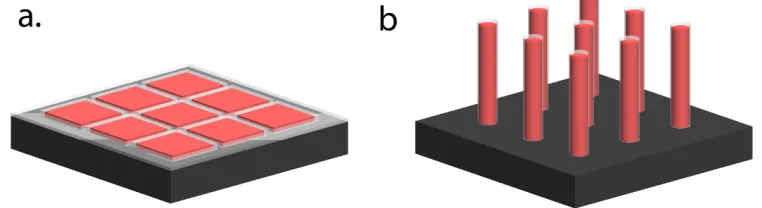
5.7 Structured Metal Island Catalysts . . . 77
5.8 Comparison of Optical Waveguides and DL-ARC Metal Island Arrays 78 5.9 Strategies for TiO2Nanocone Fabrication . . . 80
5.10 Summary and Outlook . . . 83
Chapter VI: Conclusion . . . 84
Appendix A: Methods . . . 87
Appendix B: Matlab Code for Optical Simulations . . . 88
LIST OF ILLUSTRATIONS
Number Page
1.1 Energy diagram for a tandem photovoltaic-biased electrosynthetic cell 3 1.2 Oxygen evolution for an photovoltaic-biased electrosynthetic cell . . 4 1.3 Hole conduction through a defect band within the protection layer
band gap . . . 12 1.4 Corrosion of GaAs electrodes in 1.0 M KOH . . . 13 2.1 Wafer-bonding and epitaxial liftoff process to produce ideal bandgap
combinations using single-junction III-V cells grown epitaxially on GaAs and InP . . . 19 2.2 Structure of the InGaP/GaAs tandem cell architecture using an
Al-GaAs/GaAs tunnel junction. . . 23 2.3 Non-aqueous two-electrode cyclic voltammetry of the InGaP/GaAs
tandem cell . . . 24 2.4 Solid state performance of the InGaP/GaAs tandem cell using a Ni
metal front contact . . . 25 2.5 Reflectance of InGaP/GaAs structure with varying thicknesses of TiO2 26
3.1 Fully integrated III-V unassisted water-splitting prototype. . . 28 3.2 Cross-sectional SEM image of a GaAs/InGaP/TiO2/Ni photoelectrode. 30
3.3 Module for planar photoelectrochemical devices in a louvered design system configuration . . . 33 3.4 Teflon O-Ring compression cell for aqueous photoelectrochemical
testing. . . 34 3.5 Photoelectrochemical performance of III-V water-splitting device . . 35 3.6 Long-term stability test of III-V water-splitting device with TiO2
protection layer . . . 37 3.7 Hydrogen fuel collection in unassisted water-splitting prototype . . . 38 3.8 Faradaic efficiency of water-splitting prototype . . . 40 3.9 Example of III-V device corrosion due to pinhole formation . . . 41 3.10 SEM images of device failure after 6.5 hours of operation . . . 42 3.11 Protection scheme for chemically-isolated III-V structures on a
self-passivating substrate using ALD-TiO2. . . 43
4.2 Bipolar membrane water-splitting device in 3-electrode setup . . . . 50 4.3 Bipolar membrane water-splitting device performance . . . 51 4.4 Solar-driven CO2reduction to formate using a bipolar membrane . . 55
5.1 Overview of nanocone array cell processing . . . 62 5.2 IP-Dip photoresist cone array on Glass/ITO . . . 63 5.3 Finite-Difference Time-Domain simulations of IP-Dip nanocone array 64 5.4 SEM images of IP-Dip nanocone array after Ni electrodeposition . . 65 5.5 Transmittance through square array of IP-Dip nanocones on Glass/ITO
surrounded by Ni film . . . 66 5.6 FDTD simulation of high-aspect-ratio IP-Dip nanocones in a
hexag-onal array of variable pitch on Glass/ITO . . . 68 5.7 FDTD simulation of Ni hole array on Glass/ITO . . . 69 5.8 Light management using high-aspect-ratio TiO2nanocones on Si . . 70
5.9 Transmittance to Si surface with varying nanocone tip radius . . . 71 5.10 Transmittance to Si surface varying nanocone height in solution . . . 71 5.11 Effect of Ni film on transmission to Si through TiO2nanocone
waveg-uides . . . 72 5.12 Detailed balance allocation of the AM1.5-weighted spectrum
ab-sorbed in the III-V device with optimal DL-ARC coating . . . 74 5.13 Current density versus SiO2/TiO2DL-ARC thicknesses for the
com-plete III-V PEC device . . . 76 5.14 Obscuration of non-reflective conical structures with constant
cat-alytic overpotential requirements . . . 77 5.15 Performance of TiO2nanocone array on GaAs compared to a TiO2/SiO2
DL-ARC with Ni metal island array. . . 79 5.16 Short-circuit current density and solar-to-hydrogen efficiency of TiO2
nanocone and DL-ARC Ni metal island arrays . . . 80 5.17 SEM images of TiO2 nanocone fabrication using PVD on surfaces
patterned with e-beam lithography . . . 81 5.18 Suggested processing steps for TiO2dielectric waveguides on
LIST OF TABLES
Number Page
2.1 Epitaxial structure for single-junction reversed n+-p InGaP subcell grown on GaAs. . . 20 2.2 Epitaxial structure for single-junction n+-p InGaAsP subcell grown
on InP. . . 20 2.3 Epitaxial structure for dual-junction InGaP/GaAs III-V cell. . . 21 2.4 Results from AFORS-HET 1D numerical simulation of the
NOMENCLATURE
ηST F. solar to fuel efficiency.
ηST H. solar to hydrogen efficiency.
fc. geometric catalytic filling fraction.
Eg. band gap energy.
Jsc. short-circuit current density.
Voc. open-circuit voltage.
AEM. anion-exchange membrane.
ALD. atomic layer deposition.
AM1.5. air mass 1.5 solar spectrum.
ARC. anti-reflection coating.
BPM. bipolar membrane.
CEM. cation-exchange membrane.
CO2R. carbon dioxide reduction.
CV. cyclic voltammetry.
EQE. external quantum efficiency.
FF. fill factor.
HER. hydrogen evolution reaction.
IPA. poly(isopropyl alcohol).
KOH. potassium hydroxide.
MOCVD. metal-organic chemical vapour deposition.
n++. degenerately-doped n-type material.
n+. highly-doped n-type material.
OER. oxygen evolution reaction.
p++. degenerately-doped p-type material.
PEC. phtoelectrochemical.
PMMA. poly(methyl methacrylate).
PV. photovoltaic.
SCE. saturated calomel electrode.
SEM. scanning-electron microscopy.
C h a p t e r 1
INTRODUCTION TO SOLAR FUEL DEVICES
Sunlight is an abundant renewable energy resource. However, there is a large mis-match between the availability of sunlight and peak demand for the electrical power grid. This requires efficient energy storage to enable large-scale power generation using photovoltaic solar panels. Photoelectrochemical (PEC) cells convert energy from the sun into chemical fuel, which can be stored and used on demand.
A fully-integrated photoelectrochemical water-splitting device that efficiently produces hydrogen directly from sunlight would provide a scalable, sustainable source of energy that can be used for grid storage as well as the transportation sector. In such a system all components must safely operate under mutually compatible conditions. Furthermore, a half-cell that performs water oxidation could also be used for the photoelectrochemical reduction of CO2, opening up a variety of fuel
products that can be used for energy storage.
The following chapter is an introduction to the basics of solar water splitting, and provides motivation for the creation of integrated, high-efficiency, III-V solar fuel devices that are intrinsically safe, operate in extreme pH, and use highly-active earth-abundant electrocatalysts.
1.1 Solar Fuels
The direct production of fuels from sunlight could provide scalable grid storage that would offset the intermittent nature of renewable energy sources like wind and photovoltaics. PEC systems require the following: light-absorbing materials, fuel-forming electrocatalysts, an electrolyte, and an ability to perform product separation. These materials must operate together under mutually compatible conditions, and the highest performing components cannot necessarily be combined to create a viable and efficient device [1]. In addition, there are many viable device architectures for the production of fuel from sunlight [2].
The multielectron reduction of CO2 to a liquid fuel, while more challenging
than water splitting, also promises to produce energy-dense fuels from sunlight that would be particularly useful for the transportation sector [4]. Liquid fuel requirements for ships, aircraft, and heavy-duty trucks create 40% of the current global transportation fuel demand [4], and a renewable alternative could have a significant impact on fossil fuels emissions.
Solar fuel devices for solar water splitting and CO2reduction must be efficient,
stable, cost-effective, and intrinsically safe for scalable deployment in order to demonstrate commercial viability.
1.2 Solar-Driven Water Splitting
The production of H2(g) from water and sunlight requires the electrolysis of water,
andEquation 1.1 shows the water-splitting reaction
H2O→ H2+ 1
2O2 (1.1)
which can be separated into two half reactions. In acidic conditions this is
4H++4e− → 2H2 (1.2)
2H2O→O2+4H+ +4e− (1.3) and in alkaline conditions, these half reactions become
4H2O+4e− →2H2+4OH− (1.4) 4OH− →O2+2H2O+4e− (1.5) Equations 1.2 and1.4 are referred to as the hydrogen evolution reaction (HER), and correspondingly Equations 1.3 and 1.5 are the oxygen evolution reaction (OER).
To create a semiconductor device that performs unassisted solar water splitting, the band edges of the semiconductors must straddle the electrochemical potentials E◦ (H+/H2) and E◦(O
2/H2O) in order to deliver holes and electrons to catalytic surfaces
that simultaneously drive the HER and OER. As shown inFigure 1.1, this can be accomplished using two p-n PV junctions in series that form a photovoltaic-biased electrosynthetic cell.
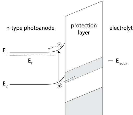
Figure 1.1: Energy diagram for a tandem photovoltaic-biased electrosynthetic cell. Electron energy (in eV) increases in the ordinate vertically. Photons absorbed in the semiconductor excite electron-hole pairs, with holes moving from the cathodic surface (left) to the anodic surface (right) of the device.
drives the OER, and, in the presence of dissolved O2(g), reductive current (-) drives
the oxygen reduction reaction (ORR). When combined with a solid state device to form a photovoltaic-biased electrosynthetic cell, also shown inFigure 1.2 (purple curve), the energy barrier created by the ideal diode behavior prevents hole conduc-tion to the surface, and OER does not occur in the dark. Upon illuminaconduc-tion, the diode behavior shifts upward due to photoexcited carriers (cyan curve inFigure 1.2 ), and anodic current drives the OER. It is important to note that the onset potential for the OER at the surface of the device does not change, it is the voltage drop across the semiconductor device that creates the shift in measured potential.
To extract the solid-state photovoltaic I-V behavior (dashed curve), load-line analysis can be performed using a simplified equivalent circuit . The electrochemical load for the device (green) can be subtracted from the, gives the dashed curve in Figure 1.2 which can give the photovoltaic parameters of the buried junctions including open-circuit voltage (Voc), short-circuit current density (Jsc), and fill
factor (FF).
The production of H2(g) fuel is subject to the constraints imposed by the
Figure 1.2: Oxygen evolution for an photovoltaic-biased electrosynthetic cell in the dark (purple) and under illumination (cyan). Anodic current drives the oxygen evolution reaction (OER), and cathodic current drives the oxygen reduction reaction (ORR). The electrochemical load of water splitting (green) has an onset for the OER at the expected electrochemical potential E◦ (O
2/H2O) at 1.23 V vs. RHE. The
solid-state photovoltaic I-V behavior (dashed curve) can be derived using load line analysis.
overpotentials, as well as entropic losses in the device. The conversion efficiency for solar water splitting devices is calculated using the thermodynamic requirement of 1.23 eV to perform water electrolysis. This solar-to-hydrogen efficiency is defined as:
η = voltagetotal input power×current density (1.6)
ηST H =
1.23 (V) × jop(mA cm−2) Stot (mW cm−2)
(1.7)
where jopis the operating short-circuit current density, andStot is the total incident solar irradiance.
1.3 Operational Criteria for Safe, Efficient Electrolyzers
Commercial electrolyzers must meet several criteria to be considered safe and reliable for operation and sale into the marketplace. They must be intrinsically safe, and not produce a flammable, potentially explosive mixture of H2(g) and O2(g)
the membrane separator, because the stoichiometry of the evolved H2and O2is 2:1.
The membrane must be able to hold back pressure because a pressure differential is required to beneficially collect the H2(g) in a pipeline, as opposed to evolving the
gas at atmospheric pressure in a laboratory demonstration device.
1.4 Discrete Photovoltaic / Electrolyzer Systems
One approach to solar-driven hydrogen production involves use of photovoltaic (PV) panels, modules or cells connected physically and electrically in series with an electrolyzer. For a combined photovoltaic/electrolyzer system, efficiency is calculated using the efficiency of the individual components, as shown inEquation 1.8.
ηST H =ηPV ×ηelectr olyzer (1.8) Commercial electrolyzers typically are designed to operate at 70% efficiency [5– 8]. To obtain optimal impedance matching in view of hourly, daily and seasonal variability in the solar irradiance, a dynamic DC-to-DC converter, with an esti-mated efficiency of 85%, would be used to connect the electrolyzer to the PV unit. Therefore a solar-to-hydrogen efficiency based on any specific PV + electrolyzer system can be estimated by taking the peak PV efficiency and multiplying by ~0.60 [9]. Thus, peak system efficiencies of 12.6% and 24.6%, respectively, could be obtained by use of an electrolyzer in conjunction with a high-efficiency (21%) Si PV module or a high-efficiency (41%) III-V triple junction PV operated under op-tical concentration [9]. Such systems have been demonstrated at commercial scale, laboratory scale, and research scale [10–17]. For example, Si PV mini-modules and perovskite-based solar cells, respectively, have been used recently in the PV + elec-trolyzer configuration[11, 12]. Significant advances include series interconnected CuInxGa1−xSe2 (CIGS) absorbers in conjunction with two Pt electrodes in 3.0 M H2SO4(aq) with a solar-to-hydrogen efficiency ηST H > 10% [10], and a bismuth vanadate photoanode in combination with a thin-film silicon solar cell has produced
ηST H = 5.2% [18]. At the commercial level, the high balance of systems cost and low capacity factor of stand-alone PV-electrolyzer systems results in high levelized hydrogen costs relative to hydrogen produced by steam reforming or grid electrolysis using fossil or low-carbon electricity [19].
1.5 Fully-Integrated Photoelectrochemical Water-Splitting Devices
of systems [1, 20–22]. Modeling and simulation has revealed a range of integrated device architectures that can allow for efficient operation and scalable deployment of solar-driven water splitting systems that can produce renewable H2(g) as an energy
carrier [22–28]. A compilation of reported devices [21] shows a wide range of efficiency, integration, and stability. Many monolithically integrated solar-driven water-splitting devices based on tandem structures or triple junctions have been described previously [21]. Some of those devices are compatible with operation in an efficient, intrinsically safe system.
“Wireless” monolithically integrated photoelectrochemical water-splitting de-vices were reported in 1977 using platinized SrTiO3[29]. However, the band gaps,
Eg, of SrTiO3 and related metal oxides are too large to allow for highly efficient
use of the solar spectrum [30]. Smaller band gap materials are generally unstable to photocorrosion in aqueous solutions, and need to be protected, generally with coatings of transparent, conductive oxides (TCO), to provide stable operation [31– 34].
TCO-coated amorphous hydrogenated Si (a-Si:H) triple junction structures have been widely explored in monolithically integrated water-splitting systems in which the photoelectrode, protection layer(s), and electrocatalytic species share a common optical path [35–37]. Use of a-Si:H triple junctions in monolithically integrated structures protected by TCOs, in conjunction with either Pt or with earth-abundant electrocatalysts for the hydrogen-evolution reaction (HER) and oxygen-evolution reaction (OER), have yielded solar-to-hydrogen efficiencies of up to 5% [35]. In monolithically integrated solar-fuels devices, tandem structures can provide significantly higher efficiencies than triple junctions [38].
Near-neutral devices
Both modeling/simulation results and experimental data have shown that electrolyz-ers operated in solutions buffered to near-neutral pH are inefficient and/or not in-trinsically safe. For example, operation of a membrane-free near-neutral pH a-Si:H device with ITO protective layers and earth-abundant, high overpotential electro-catalysts at ηST H = 3.2% produced 10% O2(g) in the cathode chamber and up to 40% H2(g) in the anode chamber, presenting an explosion hazard [39]. Introduction
buffered solutions will result in pH gradients between the anode and cathode that produce local pH changes near the electrode surfaces, due to the consumption of pro-tons associated with evolution of H2(g) from water and concomitant production of
protons associated with production of O2(g) from H2O [39, 40]. The overpotentials
associated with the pH gradients and electrodialysis exceeded the combined overpo-tentials associated with the oxygen-evolving and hydrogen-evolving electrocatalysts, precluding the construction of an efficient (photo)electrolysis system. Further mod-eling and simulation efforts have shown that active convection by bubble evolution, for example, can minimize the formation of pH gradients but results in the loss of intrinsic safety, due to the concomitant co-evolution of stoichiometric, potentially explosive, mixtures of H2(g) and O2(g) at atmospheric pressure in the reaction
ves-sel, in the presence of active catalysts for the recombination of these gases as well as in the presence of light and heat [40].
Triple junction a-Si:H devices, protected by ITO on one side in conjunction with phosphate-containing Co oxide as an OER electrocatalyst [41–44] and on the other side by stainless steel in conjunction with a Ni–Mo–Zn HER catalyst, yielded
ηST H = 1.75–2.5% for 10 h in aqueous solutions buffered to pH = 9 with borate [41]. The combined HER and OER overpotentials of the electrocatalysts at 10 mA cm−2of current density exceeded 1 V [45], and the OER catalyst delaminated from the electrode at current densities of <10 mA cm−2[46, 47], precluding construction of robust, efficient monolithically integrated devices. Moreover, such devices co-evolve stoichiometric mixtures of hydrogen and oxygen gas, precluding intrinsically safe operation.
When a cation-exchange or anion exchange membrane is included in the sys-tem, severe pH gradients and electrodialysis of the solution occurs. These effects are a consequence of the low transference number [48] at near-neutral pH of pro-tons or hydroxide ions across the membrane, relative to the transference number of other, higher concentration, charge-carrying ions in the buffered solution [39, 40]. In the absence of a membrane and with adequate convection of the electrolyte, the losses due to electrodialysis and ohmic resistance can be minimized, but po-tentially explosive mixtures of H2(g) and O2(g) are produced over active catalysts
Integrated devices operating in extreme pH
Integrated water-splitting devices that utilize a single electrolyte need to operate in extreme pH, as the unity transference number for protons or hydroxide ions in cells that include a CEM or an AEM in strongly acidic or strongly alkaline electrolytes (pH 0 or 14) minimizes the voltage lost due to resistance, pH gradients, and electrodialysis.
For example, a-Si:H triple junction devices, with RuO2on a Ti substrate used
for the OER and Pt islands deposited directly onto the a-Si:H as the HER catalyst, have been used to split water in 1.0 M H2SO4(aq) [35]. Those devices exhibited
steady-state ηST H = 5% over >4 h of operation. Triple-junction and quadruple-junction a-Si:H devices, coated with Pt as a HER catalyst and RuO2 as an OER
catalyst, have yielded ηST H = 2.6% in 5.0 M H2SO4(aq) [36, 37]. Such structures would benefit by the use of more advanced a-Si:H triple junction structures [50] that could produce higher current densities at the ~1.7 V optimal operating voltage that results from the relatively low combined HER and OER overpotentials of Pt in 1.0 M H2SO4(aq) at 10 mA cm−2of current density [51]. Such devices have the capability
of being incorporated into intrinsically safe systems because the transference number of protons in acidic media is essentially unity across gas blocking, cation-exchange membranes such as Nafion [52]. Monolithically integrated a-Si:H devices, protected on one side by ZnO in conjunction with a Co-Mo HER catalyst, and protected on the other side by SnO2in conjunction with an Fe–NiOxOER catalyst, have yielded
ηST H = 2.5–3.0% in 1.0 M KOH(aq), with stability for >18 h of operation [53]. Such devices also have the capability of operating in intrinsically safe systems, due to the essentially unity transference numbers of hydroxide ions across anion exchange membranes in alkaline media. In 1.0 M KOH(aq), the combined HER and OER Ni-based catalyst overpotentials are <0.5 V at 10 mA cm−2of current density [51]. Hence relatively high efficiency systems can potentially be achieved through improvements in the performance of the light absorber, especially in conjunction with the Ni islands on protective TiO2 films deposited by ALD. Indeed, prior
attempts to fabricate monolithically integrated solar-driven water-splitting devices and systems based on a-Si:H triple junctions in 1.0 M KOH(aq) failed due to the lack of a suitable, stable protective anode coating [41, 54, 55].
established properties of commercial electrolyzers, an intrinsically safe electrolysis or photoelectrolysis system does not produce a flammable, potentially explosive mixture of H2(g) and O2(g) in the reactor at any point in space or time. Common
TCO’s, such as indium tin oxide (ITO), are not stable in alkaline electrolytes [41, 54].
Efficient III-V photoelectrochemical devices
GaAs and other III-V semiconductors are ideal materials for photovoltaic and pho-toelectrochemical energy conversion. Many III-Vs have a direct band gap, can be epitaxially grown to produce high-quality single crystals, and can be passivated by other epitaxial III-V materials in the same growth. Single-crystalline thin films of these materials can provide a wide range of band gaps, and thus voltages, for incor-poration into a PEC device, a crucial advantage in solar fuel generation. Because catalyst performance can dramatically change the overpotential needed to drive fuel-forming electrochemical reactions, voltage requirements for water electrolysis and CO2 reduction systems can change dramatically when a complete prototype
is assembled. For the large variety in voltage demands, tunable band gaps ensure optimized device performance over a range of architectures and materials.
For example, a photovoltaic-biased photoelectrosynthetic device based on a III–V tandem structure has exhibited 12.4% solar-to- hydrogen conversion efficiency,
ηST H, under concentrated solar illumination [56]. However, III-V semiconductors are thermodynamically unstable under operating conditions and, without protection, undergo self-corrosion in alkaline and acidic environments [57]. The design of the III-V layer stack must account for t operation in solution. The III–V semiconductors photocorrode both under hydrogen-evolution reaction (HER) and oxygen–evolution reaction (OER) operating conditions [56–58], and therefore require protection to be utilized in such applications.
Tandem structures based on on InGaP/GaAs structures, but where the InGaP is exposed to the electrolyte as a photocathode, in conjunction with Pt/Ru and Pt as HER and OER electrocatalysts, respectively, have been used to produce monolithically integrated solar-driven water-splitting devices in 1.0 M H2SO4(aq) or in >1 M
protection of III-V tandems that has been the chemical and photoelectrochemical surface transformation of AlInP window layers using an aqueous solution of RhCl that serves to deposit Rh catalyst and to prevent corrosion of the underlying substrate [60]. This system decayed rapidly over time, decreasing steadily fromηST H = 17% to half of that performance over 40 hours [60]. The stability of these systems is limited due to cathodic decomposition processes characteristic of III–V materials in aqueous electrolytes [57].
Protection of III–V materials as photoanodes has also been a valuable and unrealized objective. Such devices are well-suited for use in efficient, intrinsically-safe water-splitting systems, and increases in the stability of such devices will require the development of robust protective coatings that are compatible with operation in aqueous acidic media, and/or the use of the protection schemes.
1.6 Devices for the Reduction of CO2
CO2 reduction (CO2R) involves very different optimal electrolyte conditions than
water-splitting reactions. Electrocatalysts for CO2R have been developed mainly
for near-neutral pH values [61, 62]. In alkaline conditions, the low concentration of dissolved CO2imposes severe mass-transport limitations for the cathodic CO2R
reaction, while in acidic conditions the high proton concentration favors H2(g)
production. Currently the only efficient and selective operation of CO2R catalysts in
near-neutral pH and at high operating current densities (e.g. 101 mA cm−2) involve the two-electron/two-proton reduction of CO2to produce either CO or formate. [61,
63–66].
Just as with the water-splitting cells described previously, the OER half-reaction is required to provide electrons and protons for the sustainable electrochemical re-duction of CO2[4]. Mixed-metal oxides have been extensively studied in strongly
alkaline conditions, with state-of-the-art catalysts exhibiting ~250-300 mV overpo-tentials at 10 mA cm−2of anodic current density [51, 67]. In contrast, electrocatalysts for the OER in near-neutral electrolytes exhibit substantially larger overpotentials [51, 68] because the negatively charged hydroxide ion is more readily oxidized than a neutral water molecule, and because hydroxide is present in high concentration in alkaline solutions [69]. For this reason, laboratory demonstrations of solar-driven CO2R devices at near-neutral pH values suffer substantial overpotential losses for
[64]. A polymeric Ru complex for formate generation in 0.1 M aqueous phosphate buffer achieved anηST F= 4.6% [70]. However, in addition to increased efficiencies, a full solar-driven CO2R device requires a robust means to separate the end products.
To improve efficiencies in a sustainable device, transitioning the OER catalysts to extreme pH can resolve these overpotential losses, but will require anodic protection of semiconductors in solution.
1.7 Scientific Gap
For more than four decades, the cathodic and anodic protection of small-bandgap semiconductor electrodes for use in photoelectrochemical devices has been an im-portant drive in the solar fuels community [31, 73]. Corrosion is an issue for many non-oxide semiconductors used in photoelectrochemistry, and depending on pH and potential, they exhibit either passivation, where the production of insoluble species on the exposed surface prevents further corrosion, or dissolution into surrounding medium. To date, all known non-oxide semiconductors are unstable during anodic oxygen evolution [31]. Stabilization of large-area photoelectrodes for operational lifetimes sufficient to allow practical or commercial deployment of an integrated solar fuel system requires defect-tolerant surface protection of semiconductor ma-terials.
In order to protect high-quality single-crystalline semiconductors without chang-ing their electrochemical properties for hole or electron transfer through the electrode-solution interface, many different strategies have emerged. Alternate redox couples have been added to the solution to allow a preferential electrode reaction rather than the dissolution of the semiconductor. Thin metal films have been deposited on the surface of the semiconductor, sometimes requiring constant cathodic current on the exposed III-V surface during operation for stability [56], a severe impairment for long-term stability with an intermittent energy source and the day-night cycle. Using large bandgap semiconductors like n-type TiO2, SnO2, and SrTiO, originally
used as light absorbers in low-efficiency water-splitting devices for their stability during the photo-oxidation of water, is yet another strategy towards stable device architectures.
since the 1970s Kohl:1977, and recent advances have been made towards protecting III-Vs like InP for use in solar water splitting [74] and CO2reduction [75].
1.8 Protecting Semiconductors with Hole-Conducting TiO2
The energy bands of TiO2, while aligned with the conduction band of InP and Si,
has a large valence band offset that creates a tunneling barrier for photogenerated holes [76]. Previous attempts to create oxide protection layers for photoanodes relied on a tunneling mechanism for charge carrier transfer to solution, and thus underlying layers were prone to corrosion due to pinholes in the thin oxide films [34]. While TiO2 has been used to protect semiconductors for water reduction
by taking advantage of energy band alignments for electron transport through the conduction band [77], charge transfer for water oxidation was unexpected due to the large band gap offset between the protective film and the underlying semiconductor.
Figure 1.3: Hole conduction through a defect band within the protection layer band gap. Without this miniature band, the large mismatch in valence band energies be-tween the photoanode and thick oxide protection layer would block hole conduction to the electrolyte.
Work performed at the Joint Center for Artificial Photosynthesis (JCAP) found conformal growth of thick TiO2via atomic layer deposition (ALD) can enable hole
protection layer explains the behavoir of these TiO2-coated electrodes. One of
the many advantages of using the ALD process is the conformal nature of the growth. The thickness of these films can be controlled very precisely, as each layer is assembled monolayer by monolayer. The deposition utilizes alternating gas phase chemical processes that are self-limiting, ensuring every exposed surface is covered uniformly during each step. This allows for conformal coating of not only planar films, but of any 3D structure, which enables the protection of many different cell architectures.
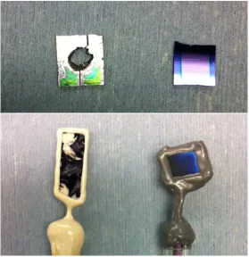
Figure 1.4: Corrosion of GaAs in 1.0 M KOH(aq) using a compression cell (top) and epoxied electrode (bottom) with and without an ALD-TiO2protection layer.
As can be seen inFigure 1.4, III-V materials that actively corrode under OER conditions in 1.0 M KOH can be successfully protected for long-term operation using amorphous TiO2films deposited using atomic-layer deposition (ALD). These films
pH will also require anodic protection, regardless of the fuel that is produced on the cathodic surface. Many constraints on the fuel production, such as large catalytic overpotential requirements, are likely to interfere with light absorption, and would necessitate illumination from the anodic side of the device. A protection scheme that chemically passivates photoanodic surfaces designed for oxygen evolution in a solar-driven water-splitting device could be modified for use as the anodic component for other purposes, such as a CO2reduction device. Thus, demonstration of a device that
incorporates a long-term stable photoanode opens up a wide number of architectures for solar fuel devices.
1.9 Contents of this Thesis
In this thesis the ALD-TiO2 protection scheme is used to create highly efficient,
stable, earth-abundant, intrinsically safe, and fully-integrated solar fuel prototypes that use high-quality III-V materials to perform unassisted solar water splitting and CO2 reduction. Light management strategies are also developed to improve
efficiencies of solar fuel devices, with potential use for a variety of optoelectronic technologies.
• In Chapter 2, two optimized III-V multijunction architectures are presented, and an MOCVD-grown high-quality InGaP/GaAs tandem cell is fabricated and characterized. Optical simulations lead to the design of a TiO2protective
coating that serves as a single-layer antireflecion coating.
• In Chapter 3, this III-V design is used to create a monolithically integrated device for solar-driven water splitting in 1.0 M KOH(aq) to achieve record sta-bility using the TiO2protective coating. A large area (1 cm2) and intrinsically
safe solar-hydrogen prototype system performed unassisted water splitting, and collection of H2(g) and O2(g) confirmed 100% faradaic efficiency.
• In Chapter 4, bipolar membranes are incorporated into PEC devices for solar water splitting and CO2reduction, enabling large pH gradients between anode
and cathode compartments. This allows for the stable pairing of previously incompatible materials leading to increased efficiency and stability.
• In Chapter 5, the properties of dielectric waveguide structures for light trapping on planar PEC surfaces are explored. Two light management schemes are designed using TiO2nanocone arrays and double-layer antireflection coatings,
C h a p t e r 2
DESIGN OF MONOLITHIC III-V LIGHT ABSORBERS FOR PEC
DEVICES
2.1 Material Choices and Constraints
Light absorbing materials selected for use in monolithically stacked, efficient, fully integrated photoelectrochemical devices must meet three major material constraints. They must (1) be high quality semiconducting materials to facilitate light absorption and carrier collection, (2) have band gaps that are within the range of interest, and (3) be stable in the electrochemical environment during operation (if they are exposed to solution). While there has been extensive work on developing materials for use in solar fuel devices, there are currently no viable materials that meet all three of these requirements [1, 31]. To achieve long-term stability, fully integrated water-splitting prototypes have generally relied on stable but inefficient light-absorbing materials. These devices generally have large band gaps that supply excess voltage for the fuel-generating reaction, resulting in low current densities and low efficiencies.
cm 2, and solution resistance of 5 ohm cm 2[81].
Multijunction III–V compound semiconductor solar cells have been the domi-nant choice for high-efficiency photovoltaic devices. This material system displays excellent optical and electronic properties, and offers a wide array of bandgaps for use in multijunction devices that can be used to achieve the bandgap combination required for high-efficiency photoelectrochemistry.
Deposition of III-V materials
Once a material system is selected, many different deposition processes are avail-able, each yielding varying quality semiconductor growths. Multi-crystalline films cut down on cell manufacturing costs, but majority and minority carrier recom-bination at grain boundaries limit conversion efficiencies. Single-crystalline films grown epitaxially using techniques like metal-organic chemical vapor deposition (MOCVD) produce higher quality semiconductor materials. To ensure single-crystalline growth and prevent the propagation of defects and dislocations through the epilayer, the semiconductor must be lattice-matched to the substrate.
Most III–V multijunction cells are grown epitaxially on either GaAs, Ge, or InP substrates. InGaP is a high-quality material often used as the top cell in triple-junction or dual-triple-junction stacks, and control of atomic ordering in the InGaP layers provides a range of bandgaps from 1.78 to 1.9 eV. Another option is AlGaAs, which has a tunable bandgap that ranges from the 1.424 eV direct-gap GaAs to the indirect 2.12 eV AlAs bandgap, all with only a small deviation in lattice constant. For the lower bandgap, the elementary compostion of quaternary InxGa1−xAsyP1−ycan be
tuned to create a film of desired bandgap in the 0.74-1.34 eV range that is lattice-matched to InP. Alternatively, metamorphic growth of a InGaP/InGaAs tandem on a Ge substrate can yield 1.78/1.26 eV bandgaps if grown on a Ge substrate using stepgraded buffer layers to account for lattice mismatch of the epilayers [60].
Epitaxial liftoff of MOCVD-grown multijunction devices
One opportunity to decrease material costs of III-V MOCVD is to utilize epitaxial liftoff (ELO) to create thin film devices [82–84]. This process has multiple benefits over conventional MOCVD growth, and the company Alta Devices has utilized this new technology to create record-breaking thin film GaAs heterojunction solar cells while significantly reducing the cost of GaAs thin film photovoltaics.
on the substrate. For growths on GaAs a layer with a high percentage of aluminum is chosen, such as AlAs (or AlxGa1−xAs with x > 0.3) that is selectively etched in hydrofluoric acid [84]. After post-treatment, this process allows reuse of the sub-strate wafer for additional epitaxial growths, which has the potential to dramatically cut down on fabrication costs by decreasing source wafer material.
This process also enables an increase in efficiency of the final device architec-ture. A more traditional multijunction cell grown on the (roughly index matched) substrate wafer only allows incident photons a single pass through the active device. Because the inactive substrate is hundreds of microns thick, any photons not ab-sorbed in the first pass will be lost to the substrate. With thin films lifted off from the substrate, a back reflector or scattering surface can be used to increase the number of passes of incident light inside the cell, allowing increased absorption in thinner films and further reducing the material cost for the growth.
While ELO avoids many of the disadvantages of regular epitaxial growth, multijunction devices grown epitaxially on a single substrate have a limited range of available bandgaps for use in PEC devices. Inverted metamorphic multijunction (IMM) growths that use ELO can help alleviate the bandgap constraints [85]; for instance, an InGaP/(In)GaAs tandem cell can be grown epitaxially on GaAs using an AlAs sacrificial liftoff layer. The composition of InGaAs junctions can be controlled though the use of metamorphic buffers, allowing bandgaps that range in principle from 0.33 eV for InAs to 1.42 eV for GaAs. However, these designs must contend with losses in material quality of all lattice-mismatched materials due to the propagation of defects after the stepgraded buffer layer.
Direct wafer bonding of independent semiconductor devices
Ternary and quaternary III-V semiconductor growths on GaAs and InP substrates can be used to create high-quality single-junction devices with a large variety of band gaps. While growths on GaAs are ideal for the 1.6-1.8 eV bandgap range described above, the 1.42 eV bandgap of GaAs is a lower bound for lattice-matched epitaxial growth; on the other hand, lattice-matched growths on InP, while ideal for a low-bandgap subcell, cannot accomodate the high-bandgap junction to deliver the voltage required to drive water electrolysis in a tandem structure.
Figure 2.1: Wafer-bonding and epitaxial liftoff process to produce ideal bandgap combinations using single-junction III-V cells grown epitaxially on GaAs and InP. (a) High-quality growth of ternary InGaP (~1.84 eV) on GaAs, and quaternary InGaAsP cell with tunable band gap. (b) Cell processing to create wafer-bonded thin film device.
the interfacial electrical conductivities and direct bonding of the heavily-doped p -GaAs/n-InP heterojunction. Subcells grown on GaAs and InP can connected in series using a wafer-bonded tunnel diode to create a multijunction device with an ideal bandgap combination.
wafer-bonding process.
2.2 Device Physics Modeling of III-V Tandem Architectures
The Helmholtz-Zentrum Berlin’s AFORS-HET simulation software for 1-D numer-ical device physics modeling of single-junction semiconductor devices was used to predict cell performance and optimize layer thickness. Material parameters for quaternary and ternary alloys were linearly interpolated from available III-V mate-rial properties. A commercial epitaxial manufacturing company Sumika Electronic Materials Inc. was consulted during the design process, and provided feedback on the capabilities of their MOCVD growth process.
No. Material Thickness (nm) Doping Density (cm−3) Dopant 9 Al0.3Ga0.7As 20 p++ >2×10¹⁹ C
8 In0.48Al0.52P 20 p+ 2×10¹⁷ Zn
7 In0.49Ga0.51P 1000 p 1×10¹⁶ Zn
6 In0.49Ga0.51P 70 n+ 1×10¹⁷ Si
5 In0.48Al0.52P 30 n+ 5×10¹⁷ Si
4 In0.49Ga0.51P 10 n+ 3×10¹⁸ Si
3 GaAs 7 n+ 5×10¹⁸ Si
2 AlAs 15 n+ 1×10¹⁸ Si
1 GaAs 50 n+ 5×10¹⁸ Si
0 GaAs Substrate n+ 5×10¹⁸ Si
Table 2.1: Epitaxial structure for single-junction reversed n+-p InGaP subcell grown on GaAs.
No. Material Thickness (nm) Doping Density (cm−3) Dopant
8 InP 30 n+ >3×10¹⁹ Si
7 In0.52Al0.48As 10 n+ 5×10¹⁸ Si
6 In0.87Ga0.13As0.28P0.72 150 n+ 1×10¹⁸ Si
5 In0.87Ga0.13As0.28P0.72 3000 p 5×10¹⁷ Zn
4 In0.52Al0.48As 10 p+ 1×10¹⁸ Zn
3 InP 30 p+ 1×10¹⁹ Zn
2 In0.53Ga0.47As 30 p+ 1×10¹⁹ Zn
1 InP 30 p+ 1×10¹⁹ Zn
0 InP Substrate p+ 1×10¹⁹ Zn
Table 2.2: Epitaxial structure for single-junction n+-p InGaAsP subcell grown on InP.
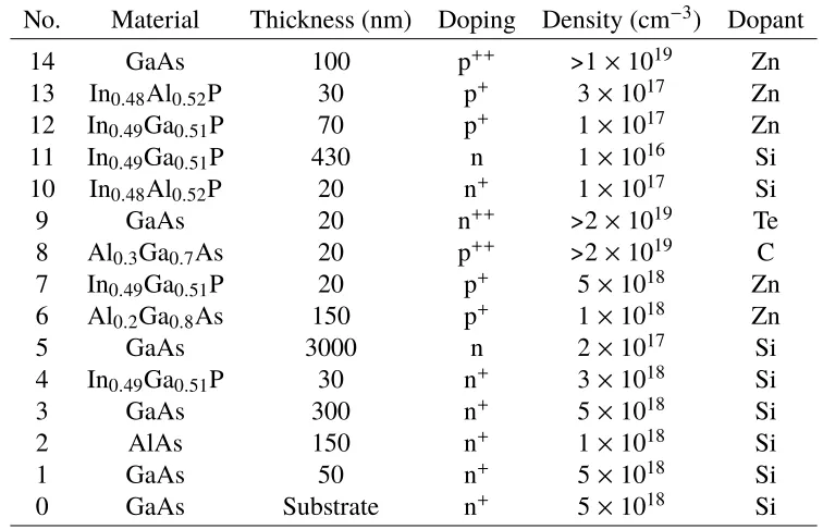
for growth on GaAs and InP substrates, respectively, and are listed inTable 2.1 and Table 2.2. The InGaP cell is grown in inverted order, with removal of the substrate using the 15 nm AlAs thin film (layer 2) as the epitaxial lifoff layer leaving behind the highly-doped 7 nm GaAs layer (layer 3) on the surface of the device. Layers 6 and 7 show the n/p solid-state buried junction. Each growth included a highly-doped thin tunnel junction layer for the wafer-bonding process. InTable 2.1 an AlGaAs layer was chosen, increasing the bandgap of the tunnel junction layer to prevent shading of the low-bandgap cell. Layer 2 in the growth on the InP substrate in Table 2.2 is meant as an etch stop layer in order to enable etching of the InP substrate layer. This allows liftoff of the bonded GaAs cell without the complications of a second liftoff step. Initial laboratory-scale demonstrations can be performued using on-wafer testing. Afterwards, with the sidewalls of the on-wafer-bonded device chemically protected, and the InP substrate can be selectively etched to produce the final thin film device. Future designs could include a sacrificial liftoff layer lattice-matched to InP instead of the etch stop layer.
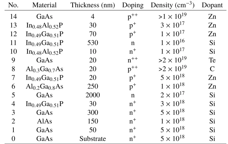
No. Material Thickness (nm) Doping Density (cm−3) Dopant
14 GaAs 100 p++ >1×10¹⁹ Zn
13 In0.48Al0.52P 30 p+ 3×10¹⁷ Zn
12 In0.49Ga0.51P 70 p+ 1×10¹⁷ Zn
11 In0.49Ga0.51P 430 n 1×10¹⁶ Si
10 In0.48Al0.52P 20 n+ 1×10¹⁷ Si
9 GaAs 20 n++ >2×10¹⁹ Te
8 Al0.3Ga0.7As 20 p++ >2×10¹⁹ C
7 In0.49Ga0.51P 20 p+ 5×10¹⁸ Zn
6 Al0.2Ga0.8As 150 p+ 1×10¹⁸ Zn
5 GaAs 3000 n 2×10¹⁷ Si
4 In0.49Ga0.51P 30 n+ 3×10¹⁸ Si
3 GaAs 300 n+ 5×10¹⁸ Si
2 AlAs 150 n+ 1×10¹⁸ Si
1 GaAs 50 n+ 5×10¹⁸ Si
0 GaAs Substrate n+ 5×10¹⁸ Si
Table 2.3: Epitaxial structure for dual-junction InGaP/GaAs III-V cell.
optimal performance under the AM1.5 spectrum, thinning of the InGaP top cell is required to allow current matching between both junction. The 100 nm surface layer of GaAs was included for solid state testing, meant to be etched away with a selective etch for use in the PEC device. However, this process created many complications in the cell fabrication process, and future iterations of this growth did not include this thick film.
The predicted cell performance and solar-to-hydrogen efficiencies of these two cell architectures are shown inTable 2.4. The remaining sections cover the growth and characterization of the higher-voltage InGaP/GaAs design that will lead to the demonstration of a full solar water-splitting device using the ALD-TiO2protection
scheme.
Subcells Bandgaps Voc(V) Jsc (mA cm−2) ηST H (%)
InGaP/InGaAsP 1.84/1.20 1.9 16.4 20.2
InGaP/GaAs 1.84/1.42 2.5 13.19 16.2
Table 2.4: Results from AFORS-HET 1D numerical simulation of the multijunction devices under the 1-sun AM1.5 solar spectrum.
2.3 Epitaxial MOCVD Growth and Cell Processing
The initial dual junction device was grown commercially through Sumika Electronic Materials, Inc. according to specifications shown inFigure reffig:VER1a. Planar III-V layers were grown epitaxially by metal-organic chemical vapor deposition (MOCVD) on an n+-GaAs wafer with a (100)-oriented polished surface with 2 deg offcut towards (110) (Si-doped, acceptor concentration of 1 × 1019 cm−3, 6"
diameter).
A tandem-junction photoabsorber consisting of an InGaP top cell (Eg = 1.84
eV) and GaAs bottom cell (Eg = 1.42 eV) was designed and modeled using a 1-D
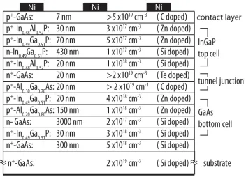
numerical simulator for operation under the Air Mass (AM) 1.5 solar spectrum [87]. Figure 2.2shows the structure of the InGaP/GaAs tandem cell. The GaAs bottom cell consisted of an n+-InGaP back surface field (BSF) layer, an n-GaAs base layer, a p+-AlGaAs emitter, and a p+-InGaP window layer. The InGaP top cell consisted of an n+-InAlP BSF layer, an n-InGaP base layer, a p+-InGaP emitter, an p+-InAlP window, and a p+-GaAs contact layer. The InGaP top cell and GaAs bottom cell were connected electrically by an GaAs/AlGaAs tunnel junction.
Figure 2.2: Structure of the InGaP/GaAs tandem cell architecture using an Al-GaAs/GaAs tunnel junction.
Ge/ 30 nm Au/ 15 nm Ni/ 100 nm Au) deposited by radio-frequency (RF) sputtering and annealed under N2(g) at 400 °C for 30 s using rapid thermal annealing.
Solid-state devices were formed by RF sputtering a metal grid of 100 nm thick Ni onto the p+-GaAs surface.
2.4 Non-Aqueous PEC Characterization
In order to test the quality of the III-V epilayer growth, especially the performance of the thin and degenerately doped layers of the n++-GaAs / p++-AlGaAs tunnel junction, our first step was to design an experiment to verify the voltage of the device under illumination. In order to avoid any cell processing on the surface of the device, which would complicate this first round of testing, initial characterization of the tandem structure was made using the ferrocene/ferrocenium (Fc/Fc+) redox couple is shown inFigure 2.3.
This characterization was performed in the inert atmosphere of a N2glovebox.
Figure 2.3: Non-aqueous two-electrode cyclic voltammetry using (a) a platinum wire, and (b) the tandem InGaP/GaAs device.
was prepared inside the glovebox, and all glass and electrode surfaces were rinsed in methanol before testing. An ELH-type W-halogen lamp was used to simulate 1-Sun illumination, and was calibrated using a Si photodiode.
Figure2.3ashows the characteristic curve that results from two-electrode cyclic voltammetry using a Pt wire as the counter electrode. InFigure 2.3bthe Pt wire was used as a reference electrode, and the result is an illuminated cyclic voltammetry (CV) curve of the III-V multijunction stack. Although this curve is not indicative of the fill factor (FF) or current density of the tandem, the open-circuit voltage (Voc) is
shown to be greater than 2.0 V, which is indicative of a good quality growth with a high-performing tunnel junction, as neither the InGaP nor the GaAs subcells could individually supply such a largeVoc.
2.5 Dual-Junction Solid State Device Performance
A Xe lamp-based solar simulator and probe station was used to measure the solid-state device performance. The light intensity was adjusted based on an NREL-calibrated Si photovoltaic reference cell.
Figure 2.4ashows the solid-state current density vs. voltage (J-V) performance of the tandem cell. Under simulated 1 sun illumination, the short-circuit current density (Jsc), the open-circuit voltage (Voc) and the fill factor (FF) were 7.6 mA cm−2, 2.4 V, and 0.76, respectively.
Figure 2.4: Solid state performance of III-V dual junction cell using a Ni metal front contact. (a) J-V performance in the dark (black) and under 1 sun illumination (red). (b) Spectral response behavior of the tandem cell, for which the integrated light-limiting current densities under AM 1.5 illumination were Jtop,int = 7.6 mA cm−2and Jbot
,int = 9.3 mA cm−2, respectively.
current limiting, and the calculated Jtop,int matched the measuredJscinFigure 2.4a. The EQE of the solid state device and the photoelectrochemical electrodes made from this III-V stack explored inChapter 3are not optimal and have room for improvement in future designs. The solid-state measurements were obtained without any surface treatment or anti-reflection coating, which results in reflection losses of ~30% for most wavelengths in the solar spectrum. A second cause of reduced EQE is parasitic absorption by the ~7 nm GaAs contact layer, which absorbs photons that have energies above the band gap of GaAs, 1.42 eV. The presence of this layer was needed to obtain facile for hole conduction through the TiO2 protection layer,
since ALD-TiO2 grown on window layers that contained exposed aluminum did
not exhibit the desired electrical properties. Simulations indicated that parasitic absorption of short wavelength light was especially detrimental to the performance of the high bandgap InGaP cell.
2.6 TiO2as an Antireflective Coating for Photoelectrochemical Devices
monochromatic beam with normal incidence is
R= r
2
1 +r22+2r1r2cos 2θ
1+r12r22+2r1r2cos 2θ (2.1) with
θ = 2πλn1d (2.2)
and wherer1andr2are
r1= n0−n1
n0+n1 , r2 =
n1−n2
n1+n2 (2.3)
with n0, n1, and n2 being the indices of refraction for the solution, antireflective layer, and substrate, respectively. The reflection is minimized whenn1d1 = λ0/4,
which gives:
Rmin =
n21−n0n2 n21+n0n2
!2
(2.4)
and is zero whenn1 =√n0n2.
For a Si (n ≈ 3.9) or InGaP (n ≈ 3.5) device in solution (nsol ≈ 1.3), the optimum refractive index for the ARC is n1 =√nsol ncell which gives an optimal index range ofn1 ≈2.0–2.2. The index of ALD-TiO2at around 600 nm is 1.9, close
to ideal for a single-layer ARC.
Figure 2.5: Reflectance of InGaP/GaAs structure with varying thicknesses of TiO2 that serves as a single-layer anti-reflection coating. Left: Optical model. Right: Integrating sphere.
In order to design the optimal thickness of TiO2, simulations were performed
and compared to experiment. Reflectance spectra of the tandem III-V substrate with TiO2coatings of different thicknesses were calculated by solving the transfer
from experimental data at http://www.ioffe.ru/SVA/NSM/nk/. The refractive index of protective TiO2 from atomic layer deposition was obtained from spectroscopic
ellipsometry. The Matlab function (multidiel), developed by Sophocles J. Orfani-dis from Rutgers University, was used to calculate the reflection responses of the isotropic lossy multilayer dielectric structures [88]. The structural information used in the calculation is shown inFigure 2.2.
The optical reflectance of the III-V tandem substrates as a function of TiO2
thick-ness (Figure 2.5) was determined by using an integrating sphere at normal incidence (Agilent Cary 5000 UV-Vis spectrometer). The absorptance (A) of TiO2-coated sub-strates was calculated from the measured total reflectance (R) and transmittance (T) of the electrode asA=1−R−T. All optical measurements were performed in air on fresh samples without chemical/electrochemical treatment. These results motivated the design of a TiO2anti-reflection coating, explored inChapter 3.
2.7 Summary
C h a p t e r 3
FULLY-INTEGRATED, HIGH-EFFICIENCY III-V DEVICE FOR
SOLAR WATER SPLITTING
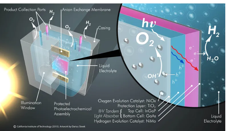
The following chapter discusses the assembly of a fully integrated, unassisted water-splitting solar fuels prototype with solar-to-hydrogen efficiencyηST H> 10%, culmi-nating in the final design shown inFigure 3.1.
Figure 3.1: Fully integrated III-V unassisted water-splitting prototype.
Content in this chapter is drawn from the following publication:
• Verlage, E., Hu, S., Liu, R., Jones, R. J. R., Sun, K., Xiang, C., Lewis, N. S. & Atwater, H. A. A monolithically integrated, intrinsically safe, 10% efficient, solar-driven water-splitting system based on active, stable earth-abundant electrocatalysts in conjunction with tandem III-V light absorbers protected by amorphous TiO2 films. Energy & Environmental Science 8,
3166–3172 (2015).
3.1 Hole Conduction Through Amorphous TiO2
It has recently been shown that thick films of amorphous TiO2 deposited using
pro-tect a variety of photoanode materials under OER conditions in alkaline electrolytes [78–80].
The sputtered Ni electrocatalyst is essential for conduction through thick layers of TiO2. While high work function metal contacts such as Ir produce lower
conduc-tivity through the TiO2film [78, 89], the deposition of low work function metals like
Ni removes the rectifying barrier of the TiO2/solution interface that blocks charge
conduction to the surface [78]. Cyclic voltammetry can be performed to age the Ni film, transforming it into NiFeOx, which is a highly-active and earth-abundant electrocatalyst.
This phenomena of hole conduction in TiO2 has previously been ascribed to
many different processes, from intrinsic conductivity through the conduction band [90], to mid-gap energy levels due to carbon and nitrogen impurities and/or Ti3+ electronic defect states [89]. This conductivity is not dependent on deposition method or the amorphous structure, as sputtered and crystalline TiO2 have been
shown to conduct charge on n-Si/TiO2/Ni photoanodes[89]. Operando X-ray
phto-electron spectroscopy performed on the Si/TiO2interface has elucidated the junction
characteristics that lead to TiO2conduction under operating conditions [91].
Current work indicates Ti3+, from oxygen vacancies or disordered structure, is responsible for creating the energetic defect states within the band gap of amorphous TiO2 [92]. Changing the TiO2 deposition processes and temperatures produces a
variety of different concentrations of Ti3+, which affects the hole conduction through these films. If the metallic top contact has a work function below ~5.2 eV, the Ti3+ states remain on the surface; however, higher work functions cause local states to be converted into Ti4+, which leads to a decrease in conductivity [92].
3.2 Design of the ALD-TiO2Protection Layer for III-V PECs
The protective films were deposited on the exposed p+-GaAs epilayer at 150 °C using an Ultratech Fiji 200 plasma atomic-layer deposition (ALD) system (Figure 3.2). In order to prevent corrosion of the III-V epilayers, care was taken to clean surfaces prior to deposition of ALD-TiO2 in order to prevent pinhole formation.
Prior to ALD, the epitaxial surface was immersed for 30 s in 1.0 M KOH (aqueous solution of potassium hydroxide pellets, semiconductor grade, 99.99% trace metals basis, Sigma-Aldrich), rinsed with copious amounts of deionized water, dried using a stream of N2(g), and loaded immediately into the ALD chamber. Each ALD cycle
0.25 s pulse of tetrakis(dimethylamido)titanium (TDMAT, Sigma-Aldrich, 99.999%, used as received). A 15 s purge under a constant 0.13 L min−1flow of research-grade Ar (g) was performed between each precursor pulse. The base pressure during the TiO2growth was maintained at ~0.1 Torr. Though care was taken to clean surfaces
to prevent defect formation in the TiO2film, and small area samples were routinely
found to be chemically passivated under operation, large area samples on the order of 1 cm2 were likely to develop at least one pinhole. The yield of stable > 1 cm2
devices was low, most likely due to particulates in the environment. Access to an ALD system in a class 100 cleanroom would likely reduce this issue, increasing yields of pinhole-free films.
Figure 3.2: Cross-sectional SEM image of a GaAs/InGaP/TiO2/Ni photoelectrode.
The results fromSection 2.6were used to select a TiO2anti-reflection coating thickness that increased current density in the current-limiting InGaP cell. While ALD-TiO2thicknesses around 62.5 nm were ideal for light absorption in the device,
thicker films were found to provide more conformal coverage to serve as a protec-tion layer. For large-area devices, thicker protecprotec-tion layers were grown to provide improved longevity during stability tests. ALD-TiO2films with thicknesses of 62.5
3.3 Catalyst and Ion-Exchange Membrane Incorporation
The scalability of III-V devices for use in solar water-splitting depends upon the exclusion of noble metal catalysts in favor of earth-abundant components, and the creation of intrinsically-safe architectures that use anion and/or cation exchange membranes avoid explosive mixtures of hydrogen and oxygen.
Electrocatalyst selection and preparation
The chemical stability and catalytic overpotential of electrocatalysts in acidic or al-kaline environments are important considerations for the design of a fully-integrated water-splitting device, and determine the electrolyte used in the final design.
Molecular electrocatalysts, both soluble and attached to an electrode, have cre-ated many systems that exhibit high turnover frequencies; however, this metric is often at the expense of catalytic overpotential [1]. On top of this, many molec-ular catalysts are active in nonaqueous electrocatalytic conditions and not stable in aqueous solutions. In the design process, we chose to focus on metal-oxide heterogeneous catalysis.
From literature, and from a comprehensive benchmarking studies by the Joint Center for Artificial Photosynthesis (JCAP) that looked at OER electrocatalysts for use in acidic and alkaline environments [51, 68], it is clear there are many earth-abundant OER electrocatalysts for use in strong base, and currently no viable options in acidic environments. The only highly active catalysts suitable for operation in acidic environments are expensive IrOxand RuOx. Until earth-abundant alternatives to Ir and Ru-based electrocatalysts are available, a photoanode that utilizes earth-abundant materials must operate in alkaline conditions.
Available active and earth-abundant OER electocatalysts that show stability in strong base include NiFeOx, CoFeOx, NiCoOx, and NiOx [51], all of which show catalytic activity that rivals that of IrOx in 1.0 M NaOH at 10 mA cm−2. Of these options, NiFeOx has the lowest overpotential. Oxidation/aging of Ni films in aqueous solutions (1.0 M KOH solution) by cyclic voltammetry, initially thought to form Ni(OH)2/NiOOH surfaces, leads to the absorption of Fe
impuri-ties in the film, causing a large increase in OER activity for these electrocatalysts [93]. In fact when the aging process is performed under inert conditions to produce Ni(OH)2/NiOOH, the activity of the film is drastically reduced [93]. In the aged