Design and Verification of Serial Peripheral Interface | ISSN: 2321-9939
IJEDR1303026
INTERNATIONAL JOURNAL OF ENGINEERING DEVELOPMENT AND RESEARCH | IJEDR Website: www.ijedr.org | Email ID: editor@ijedr.org 130Design and Verification of Serial Peripheral Interface
1
Ananthula Srinivas, 2M.Kiran Kumar, 3Jugal Kishore Bhandari 1,3
MTech Student, 2Assistant Professor
Anurag group of Institutions, Department of Electronics & Communication Engineering, JNTU, Hyderabad, AP, INDIA
1
srinivasananthula9@gmail.com, 2kirankumarece@cvsr.ac.in, 3bhandari.jugal@gmail.com
Abstarct - Today, at the low end of the Communication Protocols there are mainly Two Protocols: Inter- Integrated circuit
(I2C) and the Serial Peripheral Interface (SPI) Protocols. Both the protocols are well suited for communications between Integrated Circuits for communication with ON-Board Peripherals. SPI is one of the most commonly used serial protocols for both inter-chip and intra-chip low/medium speed data-stream transfer. In conformity with design-reuse methodology, this paper introduces high-quality SPI IP with one Master One Slave configuration with that of 8-bit data transfer which incorporates all necessary features required by modern ASIC/SoC applications. The Designed SPI is used for communication between different peripherals with that of a processor in a SoC application. The Designed SPI is Implemented and also Verified using a System Verilog in order to show its code coverage and functional correctness. The whole RTL design code is written in Verilog for synthesis and its Verification code is written in System Verilog, IEEE (2005).
Keywords - Serial Peripheral Interface (SPI), System Verilog, System- on- Chip (SoC), Intellectual Property (IP).
I. INTRODUCTION
There are many communication protocols for both short and long distance communication purpose such as ETHERNET, USB,SATA ,PCI-EXPRESS are used for long distance and I2C and SPI are used for short distance communications. SPI is a serial interface protocol, compared to other protocols, it has high transmission speed, simple to use and little pins advantages [1]. The four interfaces are required by standard SPI protocol at least. Usually, the devices which based on SPI protocol are divided into master device and slave-device for transmitting the data. The chip select signal and clock signal have be generated by the master-device when the data exchange has been processed.SPI is often considered as the “little” communication protocol which is used for ON-Board communication [2].
Although the literature on SPI protocol is so extensive and the topic is so old (early 1980), to the best of the authors knowledge there is no comprehensive analysis of SPI problem. By comprehensive analysis, we mean a treatment that start from Motorola’s V03.06 SPI bus specifications and goes down to the actual ASIC/FPGA implementation, discussing all relevant architectural aspects and providing all design details. In our attempt to implement universal SPI IP cores according to the design-reuse methodology [3], we first made a market study of an important number of recent commercial SPI devices (datasheets) from different vendors to look at the requirements and what features are to be included to satisfy modern ASIC/SoC applications.
II. SPIPROTOCOL
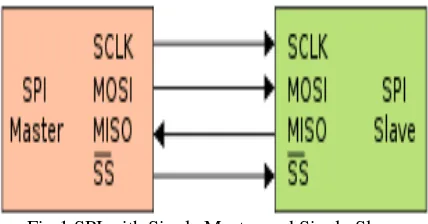
Standard SPI is a high-speed, full-duplex, synchronous communication bus [4]. For saving the chip ports and space on PCB layout, the ports of the SPI only take four lines. It is working in the Master-Slave full duplex mode which has one master device and one slave device and requires four lines whose components are SDI (data in), SDO (data out), SCK (clock), SS (Slave select) .When the SPI master wants to send data to a slave, it will pull the SS line low for selecting slave, and activates the clock signal which usable between the master and the slave at same time. The master transmits the data to the MOSI (master’s SDO and slave’s SDI) line and receives the data from the MISO (master’s SDI and slave’s SDO) line at the time. SPI is a serial communication protocol, that data is transmitted bit by bit. The clock pulse is provided by SCK and SDI, SDO is based on this pulse to making the data transmission. Data output through the master’s SDO line at the rising or falling edge of the clock, and be read by slave in the falling or rising edge followed. So 8-bit data transfer need at least 8 times the clock signal changes [3].
Fig 1 SPI with Single Master and Single Slave
SPI Signal Descriptions:Master In Slave Out (MISO)
IJEDR1303026
INTERNATIONAL JOURNAL OF ENGINEERING DEVELOPMENT AND RESEARCH | IJEDR Website: www.ijedr.org | Email ID: editor@ijedr.org 131 Table 1 SPI Interface SignalsSPI Interface Signals
PICname Master Slave
SCK Serial clock output from master [SCK] Input to Slave[SCK]
SDO Serial data output from master[MOSI] Input to slave[MOSI]
SDI Serial data input from slave [MISO] Output from slave[MISO]
SS Optional slave (chip) select [SS] Slave select [SS]
Master Out Slave In (MOSI)
The MOSI line is configured as output in a master device and as an input in a slave device. It is one of the two lines that transfer serial data in one direction, with the most significant bit sent first.
Serial Clock (SCK)
The serial clock is used to synchronize data movement both in and out of the device through its MOSI and MISO lines. The Master and Slave devices are capable of exchanging a byte of information during a sequence of eight clock cycles. Since SCK is generated by the master device, this line becomes an input on a slave device.
Slave Select (SS_bar)
The slave select input line is used to select a slave device. It has to be low prior to data transactions and must stay low for the duration of the transaction.
III. SPIDATATRANSMISSION
The SPI has four modes of operation, 0 through 3. These modes essentially control the way data is clocked in or out of an SPI device. The configuration is done by two bits in the SPI control register (SPCR). The clock polarity is specified by the CPOL control bit, which selects an active high or active low clock. The clock phase (CPHA) control bit selects one of the two fundamentally different transfer formats. To ensure a proper communication between master and slave both devices have to run in the same mode. This can require a reconfiguration of the
Table 2 SPI Modes
SPI MODE CPOL CPHA SHIFT SCK EDGE CAPTURE SCK EDGE
0 0 0 Falling Raising
1 0 1 Raising Falling
2 1 0 Raising Falling
3 1 1 Falling Raising
master to match the requirements of different peripheral slaves.
SPI is a Synchronous data transmission, Clock plays important role in this Communication. For describing the clock information we have two flags called CPOL and CPHA in SPI Control Register. The CPOL clock polarity control bit specifies an active high or low clock. The CPHA clock phase control bit selects one of two different transmission formats.
CPOL-SPI Clock Polarity Bit
To transmit data between SPI modules, the SPI modules must have identical CPOL values. In master mode, a change of this bit will abort a transmission in progress and force the SPI system into idle state.
1 = Active-low clocks selected. In idle state SCK is high. 0 = Active-high clocks selected. In idle state SCK is low.
CPHA- SPI Clock Phase Bit
This bit is used to select the SPI clock format. In master mode, a change of this bit will abort a transmission in progress and force the SPI system into idle state.
1 = Sampling of data occurs at even edges (2, 4, 6) of the SCK clock. 0 = Sampling of data occurs at odd edges (1, 3, 5) of the SCK clock.
Figure2: SPI Data Transmission of 8-bit from Master to slave
IJEDR1303026
INTERNATIONAL JOURNAL OF ENGINEERING DEVELOPMENT AND RESEARCH | IJEDR Website: www.ijedr.org | Email ID: editor@ijedr.org 132 than or equal to the maximum frequency that the slave device supports. The master then selects the desired slave for communication by pulling the chip select (SS) line of that particular slave-peripheral to low state. Data transfer is organized by using Shift register with some given word size such as 8- bits in both master and slave. They are connected in a ring. While master shifts register value out through MOSI line, the slave shifts data in to its shift register and sends data to master from slave by MISO line [6].Figure3: The timing diagram of the four different data transfer formats IV. VERIFICATIONENVIRONMENT
The Verification Plan is based on System Verilog Hardware Verification Language. The methodology used for Verification is Constraint random coverage driven verification. The Verification Plan is the focal point for defining exactly what needs to be tested and it is used to determine the progress and completion of the verification phase of verification. It will functionally verify the design with all possible corner cases. Verification plan contains the structure of the verification environment. Based on the project requirements, following points are considered while architecture is built.
• Reusability, Is it a verification IP.
• What blocks the verification language can support. • Controllability of the stimulus generation etc. • Next phase is to build the Verification environment.
• Final phase is to verify the DUT using the environment built.
Throughout these evolutionary steps, the approach to verification has not fundamentally changed. Individual design features are verified using individual test cases crafted to exercise the targeted feature.
Figure 4: Verification Environment
IJEDR1303026
INTERNATIONAL JOURNAL OF ENGINEERING DEVELOPMENT AND RESEARCH | IJEDR Website: www.ijedr.org | Email ID: editor@ijedr.org 133 Functional coverage of design features have been exercised by the tests. The process of measuring and using functional coverage consists several steps. First, add code to the testbench to monitor the stimulus going into device, and its reaction and response, to determine what functionality has been exercised and after running simulation, analyze the coverage results and find out if some test Scenarios have not been exercised and write tests to exercise them.V. IMPLEMENTATIONANDSIMULATIONRESULTS
The whole design code, either for synthesis or functional verification, is implemented in Verilog 2001 (IEEE 1365). The synthesis design code is technology independent and was simulated at both RTL and gate level (post place & route netlist) with timing back annotation using Questasim 6.2 and mapped onto Xilinx Vertex 5 FPGA using Foundation Xilinx Vivado tool.
Figure 5: RTL Schematic of Top module showing blocks of individual master and slave.
Simulation Results:
Figure 6: Overall Output waveform showing Full Duplex operation of the top module.
As that of the data transmission formats of the SPI protocol we have generated the outputs showing that it works in a full duplex operation. That is the Master’s 8-bit data is going to be stored in the fifo_read_final _slave signal after 8 clock pulses and at the same time the 8-bit data present in the slave is transferred to the fifo_read_final_master signal. We have also shown the individual MOSI and MISO outputs of the master and slave Modules. The below shown figures are the individual mode output of the SPI with that of different 8-bit data for each mode.
IJEDR1303026
INTERNATIONAL JOURNAL OF ENGINEERING DEVELOPMENT AND RESEARCH | IJEDR Website: www.ijedr.org | Email ID: editor@ijedr.org 134 Figure 9: Output of SPI Mode – 3Figure10: Output of SPI Mode – 4
Flow Chart of the Design
Verification Results:
IJEDR1303026
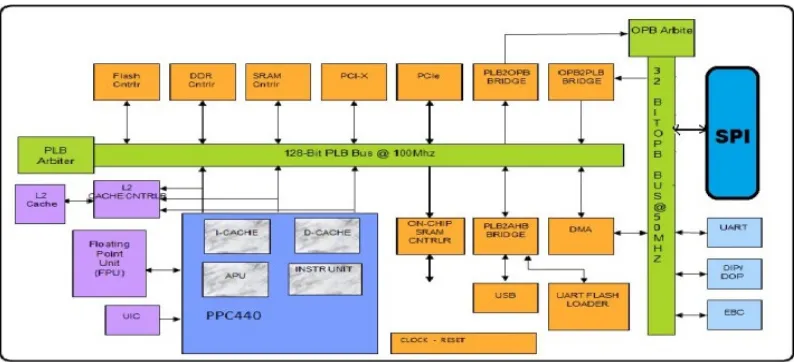
INTERNATIONAL JOURNAL OF ENGINEERING DEVELOPMENT AND RESEARCH | IJEDR Website: www.ijedr.org | Email ID: editor@ijedr.org 135 Fig 11: A SOC where the Designed SPI is used.Questa Coverage Report
Parameter Coverage Report
The main Advantage of going for SystemVerilog Verification is that of its Reusability and advanced features of OOPS concepts and constrained Randomization makes it easy to understand and make sure that the there is much coverage of code for the much more number of test cases.
Code Coverage Report
Functional Coverage Report
VI. CONCLUSION
The Design of Serial Peripheral Interface(SPI) with Single Master and Single Slave configuration has been done Successfully showing that it operates in Full Duplex Mode and also verified the Designed SPI using System Verilog using constrained Random methodology with that of 100 percentage of Code Coverage report and with all the functional coverage.
IJEDR1303026
INTERNATIONAL JOURNAL OF ENGINEERING DEVELOPMENT AND RESEARCH | IJEDR Website: www.ijedr.org | Email ID: editor@ijedr.org 136 REFERENCES[1] S.Sarns and J. Woehr, “Exploring I2C,” Embedded Systems Programming, vol. 4, p. 46, Sept. 1991.
[2] F.Leens, “An Introduction to I2C and SPI Protocols,”IEEE Instrumentation & Measurement Magazine, pp. 8-13, February 2009.
[3] Freescale Semiconductor, (2008, October 14). Freescale SPI Block Guide V04.01 July.
[4] L.Bacciarelli et al, “Design, Testing and Prototyping of a Software Programmable I2C/SPI IP on AMBA Bus,” Conference on Ph.D. Research in Microelectronics and Electronics (PRIME'2006), pp. 373- 376, ISBN: 1-4244-0157-7, Ortanto, Italy, June 2006.
[5] A.K. Oudjida et al, “FPGA Implementation of I2C and SPI Protocols: A Comparative Study”. Proceedings of the 16th edition of the IEEE International Conference on Electronics Circuits and Systems ICECS, pp. 507 -510, ISBN: 978-1-4244-5091-6, December 13-16 2009, Yasmine Hammamet, Tunisia.
[6] IP Design of Universal Multiple Devices SPI Interface Tianxiang Liu1, Yunfeng Wang1 * Department of Electronic Engineering, Xiamen University,2011 IEEE.
[7] Chris Spears SYSTEMVERILOG FOR VERIFICATION, Publisher: Springer. [8] Bhaskar. J, A Verilog HDL Primer, Publisher: Syndicate Publications.
AUTHORS PROFILES
Mr.ANANTHULA SRINIVAS , Pursuing M.TECH (VLSI System Design) from CVSR College of Engineering, Ghatkesar, Hyderabad, A.P. Completed B.Tech in Electronics and Communication Engineering from CMR Institute of Technology, JNTUH.
Mr. M KIRAN KUMAR, Assistant Professor from Anurag Group of Institutions also Worked as a Project Engineer at RCI Lab, DRDO for One Year. M.Tech from ASR College of Engineering, JNTUK Kakinada.