Device Selection Table
Features
• Single supply with operation down to 1.8V • Low-power CMOS technology
- 1 mA active current typical
- 1µA standby current typical (I-temp)
• Organized as 1 block of 256 bytes (1 x 256 x 8) • 2-wire serial interface bus, I2C™ compatible • Schmitt Trigger inputs for noise suppression • Output slope control to eliminate ground bounce • 100 kHz (24AA02) and 400 kHz (24LC02B)
compatibility
• Self-timed write cycle (including auto-erase) • Page write buffer for up to 8 bytes
• 2 ms typical write cycle time for page write • Hardware write-protect for entire memory • Can be operated as a serial ROM • Factory programming (QTP) available • ESD protection > 4,000V
• 1,000,000 erase/write cycles • Data retention > 200 years
• 8-lead PDIP, SOIC, TSSOP and MSOP packages • 5-lead SOT-23 package
• Pb-free finish available
• Available for extended temperature ranges: - Industrial (I): -40°C to +85°C
- Automotive (E): -40°C to +125°C
Description
The Microchip Technology Inc. 24AA02/24LC02B (24XX02*) is a 2 Kbit Electrically Erasable PROM. The device is organized as one block of 256 x 8-bit memory with a 2-wire serial interface. Low-voltage design permits operation down to 1.8V, with standby and active currents of only 1µA and 1 mA, respectively. The 24XX02 also has a page write capability for up to 8 bytes of data. The 24XX02 is available in the standard 8-pin PDIP, surface mount SOIC, TSSOP and MSOP packages and is also available in the 5-lead SOT-23 package.
Package Types
Block Diagram
Part Number VCC Range Max Clock Frequency Temp Ranges 24AA02 1.8-5.5 400 kHz(1) I 24LC02B 2.5-5.5 400 kHz I, E Note 1: 100 kHz for VCC <2.5V 24 XX02 A0 A1 A2 Vss 1 2 3 4 8 7 6 5 Vcc WP SCL SDA PDIP/SOIC/TSSOP/MSOP SOT-23-5 1 5 4 3 2 4 XX02 SCL Vss SDA WP Vcc 2Note: Pins A0, A1 and A2 are not used by the 24XX02. (No internal connections).
HV EEPROM Array Page YDEC XDEC Sense Amp. Memory Control Logic I/O Control Logic I/O WP SDA SCL VCC V Latches Generator
2K I
2
C
™
Serial EEPROM
1.0
ELECTRICAL CHARACTERISTICS
Absolute Maximum Ratings
(†)VCC...6.5V All inputs and outputs w.r.t. VSS... -0.3V to VCC +1.0V Storage temperature ...-65°C to +150°C Ambient temperature with power applied ...-65°C to +125°C ESD protection on all pins...≥ 4 kV
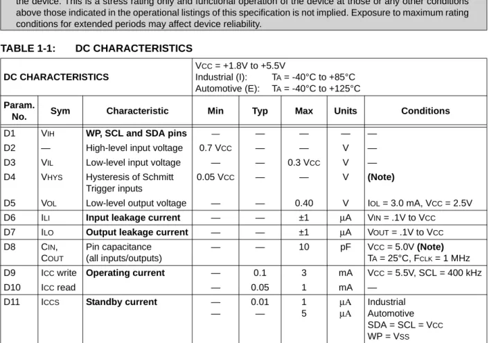
TABLE 1-1: DC CHARACTERISTICS
† NOTICE: Stresses above those listed under “Absolute Maximum Ratings” may cause permanent damage to the device. This is a stress rating only and functional operation of the device at those or any other conditions above those indicated in the operational listings of this specification is not implied. Exposure to maximum rating conditions for extended periods may affect device reliability.
DC CHARACTERISTICS
VCC = +1.8V to +5.5V
Industrial (I): TA = -40°C to +85°C Automotive (E): TA = -40°C to +125°C
Param.
No. Sym Characteristic Min Typ Max Units Conditions
D1 VIH WP, SCL and SDA pins — — — — —
D2 — High-level input voltage 0.7 VCC — — V — D3 VIL Low-level input voltage — — 0.3 VCC V — D4 VHYS Hysteresis of Schmitt
Trigger inputs
0.05 VCC — — V (Note)
D5 VOL Low-level output voltage — — 0.40 V IOL = 3.0 mA, VCC = 2.5V
D6 ILI Input leakage current — — ±1 µA VIN = .1V to VCC
D7 ILO Output leakage current — — ±1 µA VOUT = .1V to VCC
D8 CIN, COUT Pin capacitance (all inputs/outputs) — — 10 pF VCC = 5.0V (Note) TA = 25°C, FCLK = 1 MHz
D9 ICC write Operating current — 0.1 3 mA VCC = 5.5V, SCL = 400 kHz
D10 ICC read — 0.05 1 mA — D11 ICCS Standby current — — 0.01 — 1 5 µΑ µΑ Industrial Automotive SDA = SCL = VCC WP = VSS Note: This parameter is periodically sampled and not 100% tested.
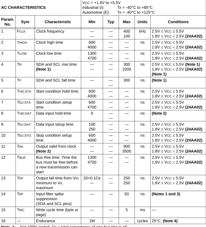
TABLE 1-2: AC CHARACTERISTICS AC CHARACTERISTICS VCC = +1.8V to +5.5V Industrial (I): TA = -40°C to +85°C Automotive (E): TA = -40°C to +125°C Param.
No. Sym Characteristic Min Typ Max Units Conditions
1 FCLK Clock frequency — — — — 400 100 kHz 2.5V ≤ VCC≤ 5.5V 1.8V ≤ VCC< 2.5V (24AA02) 2 THIGH Clock high time 600
4000 — — — — ns 2.5V ≤ VCC≤ 5.5V 1.8V ≤ VCC< 2.5V (24AA02) 3 TLOW Clock low time 1300
4700 — — — — ns 2.5V ≤ VCC≤ 5.5V 1.8V ≤ VCC< 2.5V (24AA02) 4 TR SDA and SCL rise time
(Note 1) — — — — 300 1000 ns 2.5V ≤ VCC≤ 5.5V (Note 1) 1.8V ≤ VCC< 2.5V (24AA02) (Note 1)
5 TF SDA and SCL fall time — — —
300 ns (Note 1)
6 THD:STA Start condition hold time 600 4000 — — — — ns 2.5V ≤ VCC≤ 5.5V 1.8V ≤ VCC< 2.5V (24AA02) 7 TSU:STA Start condition setup
time 600 4700 — — — — ns 2.5V ≤ VCC≤ 5.5V 1.8V ≤ VCC< 2.5V (24AA02) 8 THD:DAT Data input hold time 0 —
—
— ns (Note 2)
9 TSU:DAT Data input setup time 100 250 — — — — ns 2.5V ≤ VCC≤ 5.5V 1.8V ≤ VCC< 2.5V (24AA02) 10 TSU:STO Stop condition setup
time 600 4000 — — — — ns 2.5V ≤ VCC≤ 5.5V 1.8V ≤ VCC< 2.5V (24AA02) 11 TAA Output valid from clock
(Note 2) — — — — 900 3500 ns 2.5V ≤ VCC≤ 5.5V 1.8V ≤ VCC< 2.5V (24AA02) 12 TBUF Bus free time: Time the
bus must be free before a new transmission can start 1300 4700 — — — — ns 2.5V ≤ VCC≤ 5.5V 1.8V ≤ VCC< 2.5V (24AA02)
13 TOF Output fall time from VIH
minimum to VIL maximum 20+0.1CB — — — 250 250 ns 2.5V ≤ VCC≤ 5.5V 1.8V ≤ VCC< 2.5V (24AA02) 14 TSP Input filter spike
suppression (SDA and SCL pins)
— — 50 ns (Notes 1 and 3)
15 TWC Write cycle time (byte or page)
— — 5 ms —
16 — Endurance 1M — — cycles 25°C, (Note 4)
Note 1: Not 100% tested. CB = total capacitance of one bus line in pF.
2: As a transmitter, the device must provide an internal minimum delay time to bridge the undefined region (minimum 300 ns) of the falling edge of SCL to avoid unintended generation of Start or Stop conditions.
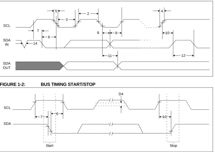
FIGURE 1-1: BUS TIMING DATA
FIGURE 1-2: BUS TIMING START/STOP
7 5 2 4 8 9 10 12 11 14 6 SCL SDA IN SDA OUT 3 7 6 D4 10 Start Stop SCL SDA
2.0
FUNCTIONAL DESCRIPTION
The 24XX02 supports a bidirectional, 2-wire bus and data transmission protocol. A device that sends data onto the bus is defined as transmitter, while a device receiving data is defined as a receiver. The bus has to be controlled by a master device which generates the serial clock (SCL), controls the bus access and gener-ates the Start and Stop conditions, while the 24XX02 works as slave. Both master and slave can operate as transmitter or receiver, but the master device determines which mode is activated.
3.0
BUS CHARACTERISTICS
The following bus protocol has been defined: • Data transfer may be initiated only when the bus
is not busy.
• During data transfer, the data line must remain stable whenever the clock line is high. Changes in the data line while the clock line is high will be interpreted as a Start or Stop condition.
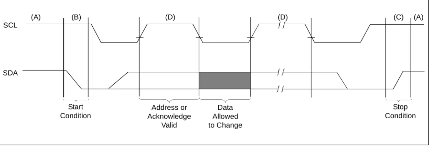
Accordingly, the following bus conditions have been defined (Figure 3-1).
3.1
Bus not Busy (A)
Both data and clock lines remain high.
3.2
Start Data Transfer (B)
A high-to-low transition of the SDA line while the clock (SCL) is high determines a Start condition. All commands must be preceded by a Start condition.
3.3
Stop Data Transfer (C)
A low-to-high transition of the SDA line while the clock (SCL) is high determines a Stop condition. All operations must be ended with a Stop condition.
3.4
Data Valid (D)
The state of the data line represents valid data when, after a Start condition, the data line is stable for the duration of the high period of the clock signal.
The data on the line must be changed during the low period of the clock signal. There is one clock pulse per bit of data.
Each data transfer is initiated with a Start condition and terminated with a Stop condition. The number of data bytes transferred between Start and Stop conditions is determined by the master device and is, theoretically, unlimited (although only the last sixteen will be stored when doing a write operation). When an overwrite does occur, it will replace data in a first-in first-out (FIFO) fashion.
3.5
Acknowledge
Each receiving device, when addressed, is obliged to generate an acknowledge after the reception of each byte. The master device must generate an extra clock pulse which is associated with this Acknowledge bit.
The device that acknowledges has to pull down the SDA line during the acknowledge clock pulse in such a way that the SDA line is stable low during the high period of the acknowledge related clock pulse. Of course, setup and hold times must be taken into account. During reads, a master must signal an end of data to the slave by not generating an Acknowledge bit on the last byte that has been clocked out of the slave. In this case, the slave (24XX02) will leave the data line high to enable the master to generate the Stop condition.
FIGURE 3-1: DATA TRANSFER SEQUENCE ON THE SERIAL BUS
Note: The 24XX02 does not generate any
Acknowledge bits if an internal programming cycle is in progress.
SCL
SDA
3.6
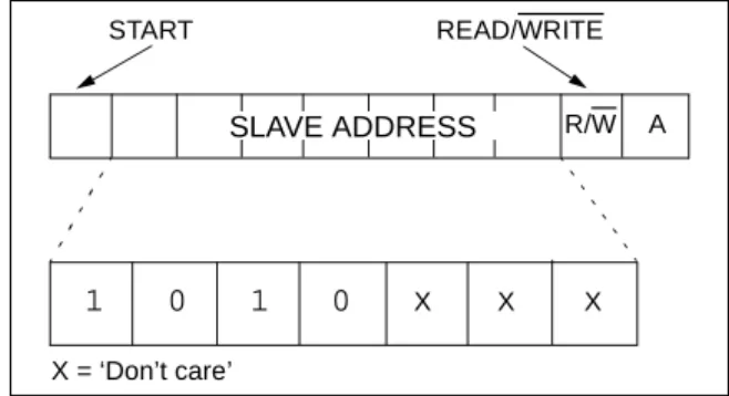
Device Addressing
A control byte is the first byte received following the Start condition from the master device. The control byte consists of a four-bit control code. For the 24XX02, this is set as ‘1010’ binary for read and write operations. The next three bits of the control byte are ‘don’t care’s’ for the 24XX02.
The last bit of the control byte defines the operation to be performed. When set to ‘1’, a read operation is selected. When set to ‘0’, a write operation is selected. Following the Start condition, the 24XX02 monitors the SDA bus checking the device type identifier being transmitted and, upon a ‘1010’ code, the slave device outputs an Acknowledge signal on the SDA line. Depending on the state of the R/W bit, the 24XX02 will select a read or write operation.
FIGURE 3-2: CONTROL BYTE ALLOCATION
Operation Control
Code Block Select R/W
Read 1010 Block Address 1
Write 1010 Block Address 0
1 0 1 0 X X X
R/W A
START READ/WRITE
SLAVE ADDRESS
4.0
WRITE OPERATION
4.1
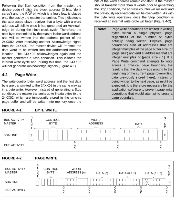
Byte Write
Following the Start condition from the master, the device code (4 bits), the block address (3 bits, ‘don’t cares’) and the R/W bit which is a logic low, is placed onto the bus by the master transmitter. This indicates to the addressed slave receiver that a byte with a word address will follow once it has generated an Acknowl-edge bit during the ninth clock cycle. Therefore, the next byte transmitted by the master is the word address and will be written into the address pointer of the 24XX02. After receiving another Acknowledge signal from the 24XX02, the master device will transmit the data word to be written into the addressed memory location. The 24XX02 acknowledges again and the master generates a Stop condition. This initiates the internal write cycle and, during this time, the 24XX02 will not generate Acknowledge signals (Figure 4-1).
4.2
Page Write
The write-control byte, word address and the first data byte are transmitted to the 24XX02 in the same way as in a byte write. However, instead of generating a Stop condition, the master transmits up to 8 data bytes to the 24XX02, which are temporarily stored in the on-chip page buffer and will be written into memory once the
master has transmitted a Stop condition. Upon receipt of each word, the four lower-order address pointer bits are internally incremented by ‘1’. The higher-order 7 bits of the word address remain constant. If the master should transmit more than 8 words prior to generating the Stop condition, the address counter will roll over and the previously received data will be overwritten. As with the byte write operation, once the Stop condition is received an internal write cycle will begin (Figure 4-2).
FIGURE 4-1: BYTE WRITE
FIGURE 4-2: PAGE WRITE
Note: Page write operations are limited to writing bytes within a single physical page
regardless of the number of bytes
actually being written. Physical page boundaries start at addresses that are integer multiples of the page buffer size (or ‘page size’) and end at addresses that are integer multiples of [page size - 1]. If a Page Write command attempts to write across a physical page boundary, the result is that the data wraps around to the beginning of the current page (overwriting data previously stored there), instead of being written to the next page, as might be expected. It is therefore necessary for the application software to prevent page write operations that would attempt to cross a page boundary. S P BUS ACTIVITY MASTER SDA LINE BUS ACTIVITY S T A R T S T O P CONTROL BYTE WORD ADDRESS DATA A C K A C K A C K S P BUS ACTIVITY MASTER SDA LINE BUS ACTIVITY S T A R T CONTROL BYTE WORD
ADDRESS (n) DATA (n) DATA (n + 7)
S T O P A C K A C K A C K A C K A C K DATA (n + 1)
5.0
ACKNOWLEDGE POLLING
Since the device will not acknowledge during a write cycle, this can be used to determine when the cycle is complete (this feature can be used to maximize bus throughput). Once the Stop condition for a Write command has been issued from the master, the device initiates the internally-timed write cycle and ACK polling can then be initiated immediately. This involves the master sending a Start condition followed by the control byte for a Write command (R/W = 0). If the device is still busy with the write cycle, no ACK will be returned. If the cycle is complete, the device will return the ACK and the master can then proceed with the next Read or Write command. See Figure 5-1 for a flow diagram of this operation.
FIGURE 5-1: ACKNOWLEDGE POLLING FLOW
6.0
WRITE PROTECTION
The 24XX02 can be used as a serial ROM when the WP pin is connected to VCC. Programming will be inhibited and the entire memory will be write-protected.
Send Write Command
Send Stop Condition to Initiate Write Cycle
Send Start
Send Control Byte with R/W = 0 Did Device Acknowledge (ACK = 0)? Next Operation No Yes
7.0
READ OPERATION
Read operations are initiated in the same way as write operations, with the exception that the R/W bit of the slave address is set to ‘1’. There are three basic types of read operations: current address read, random read and sequential read.
7.1
Current Address Read
The 24XX02 contains an address counter that main-tains the address of the last word accessed, internally incremented by ‘1’. Therefore, if the previous access (either a read or write operation) was to address n, the next current address read operation would access data from address n + 1. Upon receipt of the slave address with R/W bit set to ‘1’, the 24XX02 issues an acknowl-edge and transmits the 8-bit data word. The master will not acknowledge the transfer but does generate a Stop condition and the 24XX02 discontinues transmission (Figure 7-1).
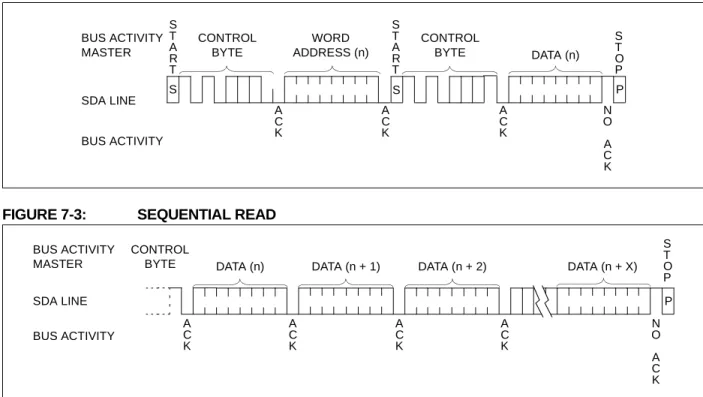
7.2
Random Read
Random read operations allow the master to access any memory location in a random manner. To perform this type of read operation, the word address must first be set. This is accomplished by sending the word address to the 24XX02 as part of a write operation. Once the word address is sent, the master generates a Start condition following the acknowledge. This terminates the write operation, but not before the inter-nal address pointer is set. The master then issues the control byte again, but with the R/W bit set to a ‘1’. The 24XX02 will then issue an acknowledge and transmit the 8-bit data word. The master will not acknowledge the transfer but does generate a Stop condition and the 24XX02 will discontinue transmission (Figure 7-2).
7.3
Sequential Read
Sequential reads are initiated in the same way as a random read, except that once the 24XX02 transmits the first data byte, the master issues an acknowledge as opposed to a Stop condition in a random read. This directs the 24XX02 to transmit the next sequentially-addressed 8-bit word (Figure 7-3).
To provide sequential reads, the 24XX02 contains an internal address pointer that is incremented by one upon completion of each operation. This address pointer allows the entire memory contents to be serially read during one operation.
7.4
Noise Protection
The 24XX02 employs a VCC threshold detector circuit which disables the internal erase/write logic if the VCC
is below 1.5V at nominal conditions.
The SCL and SDA inputs have Schmitt Trigger and filter circuits which suppress noise spikes to assure proper device operation, even on a noisy bus.
FIGURE 7-1: CURRENT ADDRESS READ
S P BUS ACTIVITY MASTER SDA LINE BUS ACTIVITY S T O P CONTROL BYTE DATA (n) A C K N O A C K S T A R T
FIGURE 7-2: RANDOM READ
FIGURE 7-3: SEQUENTIAL READ
S S P BUS ACTIVITY MASTER SDA LINE BUS ACTIVITY S T A R T S T O P CONTROL BYTE A C K WORD ADDRESS (n) CONTROL BYTE S T A R T DATA (n) A C K A C K N O A C K P BUS ACTIVITY MASTER SDA LINE BUS ACTIVITY S T O P CONTROL BYTE A C K N O A C K
DATA (n) DATA (n + 1) DATA (n + 2) DATA (n + X)
A C K A C K A C K
8.0
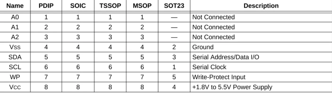
PIN DESCRIPTIONS
The descriptions of the pins are listed in Table 8-1.
TABLE 8-1: PIN FUNCTION TABLE
8.1
Serial Address/Data Input/Output
(SDA)
SDA is a bidirectional pin used to transfer addresses and data into and out of the device. Since it is an open-drain terminal, the SDA bus requires a pull-up resistor to VCC (typical 10 kΩ for 100 kHz, 2 kΩ for 400 kHz). For normal data transfer, SDA is allowed to change only during SCL low. Changes during SCL high are reserved for indicating Start and Stop conditions.
8.2
Serial Clock (SCL)
The SCL input is used to synchronize the data transfer to and from the device.
8.3
Write-Protect (WP)
The WP pin must be connected to either VSS or VCC. If tied to VSS, normal memory operation is enabled (read/write the entire memory 00-FF).
If tied to VCC, write operations are inhibited. The entire memory will be write-protected. Read operations are not affected.
This feature allows the user to use the 24XX02 as a serial ROM when WP is enabled (tied to VCC).
8.4
A0, A1, A2
These A0, A1 and A2 pins are not used by the 24XX02. They may be left floating or tied to either VSS or VCC.
Name PDIP SOIC TSSOP MSOP SOT23 Description
A0 1 1 1 1 — Not Connected
A1 2 2 2 2 — Not Connected
A2 3 3 3 3 — Not Connected
VSS 4 4 4 4 2 Ground
SDA 5 5 5 5 3 Serial Address/Data I/O
SCL 6 6 6 6 1 Serial Clock
WP 7 7 7 7 5 Write-Protect Input
9.0
PACKAGING INFORMATION
9.1
Package Marking Information
XXXXXXXX XXXXXNNN YYWW
8-Lead PDIP (300 mil) Example:
8-Lead SOIC (150 mil) Example:
XXXXXXXX XXXXYYWW NNN
8-Lead TSSOP Example:
24LC02B I/P13F 0327 24LC02B I/SN0327 13F
8-Lead MSOP Example:
XXXX XYWW NNN XXXXXX YWWNNN 4L02 I327 13F 4L02BI 32713F
5-Lead SOT-23 Example:
XXNN
M23F
Part Number TSSOP/MSOP Marking Codes STD Pb-Free24AA02 4A02 G4A2
24LC02B 4L02 G4L2 Part Number SOT-23 Marking Codes STD Pb-Free 24AA02 B2 B2 24LC02B-I M2 M2 24LC02B-E N2 N2
Note: Pb-free part number using “G” suffix is marked on carton.
8-Lead Plastic Dual In-line (P) – 300 mil (PDIP) B1 B A1 A L A2 p α E eB β c E1 n D 1 2
Units INCHES* MILLIMETERS
Dimension Limits MIN NOM MAX MIN NOM MAX
Number of Pins n 8 8
Pitch p .100 2.54
Top to Seating Plane A .140 .155 .170 3.56 3.94 4.32
Molded Package Thickness A2 .115 .130 .145 2.92 3.30 3.68
Base to Seating Plane A1 .015 0.38
Shoulder to Shoulder Width E .300 .313 .325 7.62 7.94 8.26
Molded Package Width E1 .240 .250 .260 6.10 6.35 6.60
Overall Length D .360 .373 .385 9.14 9.46 9.78
Tip to Seating Plane L .125 .130 .135 3.18 3.30 3.43
Lead Thickness c .008 .012 .015 0.20 0.29 0.38
Upper Lead Width B1 .045 .058 .070 1.14 1.46 1.78
Lower Lead Width B .014 .018 .022 0.36 0.46 0.56
Overall Row Spacing § eB .310 .370 .430 7.87 9.40 10.92
Mold Draft Angle Top α 5 10 15 5 10 15
Mold Draft Angle Bottom β 5 10 15 5 10 15
* Controlling Parameter Notes:
Dimensions D and E1 do not include mold flash or protrusions. Mold flash or protrusions shall not exceed JEDEC Equivalent: MS-001
Drawing No. C04-018 .010” (0.254mm) per side. § Significant Characteristic
8-Lead Plastic Small Outline (SN) – Narrow, 150 mil (SOIC)
Foot Angle φ 0 4 8 0 4 8
β 0 12 15 0 12 15 α
Mold Draft Angle Top
0.51 0.42 0.33 .020 .017 .013 B Lead Width 0.25 0.23 0.20 .010 .009 .008 c Lead Thickness 0.76 0.62 0.48 .030 .025 .019 L Foot Length 0.51 0.38 0.25 .020 .015 .010 h Chamfer Distance 5.00 4.90 4.80 .197 .193 .189 D Overall Length 3.99 3.91 3.71 .157 .154 .146 E1 Molded Package Width
6.20 6.02 5.79 .244 .237 .228 E Overall Width 0.25 0.18 0.10 .010 .007 .004 A1 Standoff § 1.55 1.42 1.32 .061 .056 .052 A2 Molded Package Thickness
1.75 1.55 1.35 .069 .061 .053 A Overall Height 1.27 .050 p Pitch 8 8 n Number of Pins MAX NOM MIN MAX NOM MIN Dimension Limits MILLIMETERS INCHES* Units 2 1 D n p B E E1 h L β c 45° φ A2 α A A1
8-Lead Plastic Thin Shrink Small Outline (ST) – 4.4 mm (TSSOP) 10 5 0 10 5 0 β
Mold Draft Angle Bottom
10 5 0 10 5 0 α
Mold Draft Angle Top
0.30 0.25 0.19 .012 .010 .007 B Lead Width 0.20 0.15 0.09 .008 .006 .004 c Lead Thickness 0.70 0.60 0.50 .028 .024 .020 L Foot Length 3.10 3.00 2.90 .122 .118 .114 D Molded Package Length
4.50 4.40 4.30 .177 .173 .169 E1 Molded Package Width
6.50 6.38 6.25 .256 .251 .246 E Overall Width 0.15 0.10 0.05 .006 .004 .002 A1 Standoff § 0.95 0.90 0.85 .037 .035 .033 A2 Molded Package Thickness
1.10 .043 A Overall Height 0.65 .026 p Pitch 8 8 n Number of Pins MAX NOM MIN MAX NOM MIN Dimension Limits MILLIMETERS* INCHES Units α A2 A A1 L c β φ 1 2 D n p B E E1 Foot Angle φ 0 4 8 0 4 8 * Controlling Parameter Notes:
Dimensions D and E1 do not include mold flash or protrusions. Mold flash or protrusions shall not exceed .005” (0.127mm) per side.
JEDEC Equivalent: MO-153 Drawing No. C04-086 § Significant Characteristic
8-Lead Plastic Micro Small Outline Package (MS) (MSOP) D A A1 L c (F) α A2 E1 E p B n 1 2 φ β .037 REF F Footprint (Reference)
Mold Draft Angle Top Foot Angle Lead Width Lead Thickness α c B φ .003 .009 .006 .012 Dimension Limits Overall Height
Molded Package Thickness
Molded Package Width Overall Length Foot Length Standoff Overall Width Number of Pins Pitch A L E1 D A1 E A2 .016 .024 .118 BSC .118 BSC .000 .030 .193 TYP. .033 MIN p n Units .026 BSC NOM 8 INCHES 0.95 REF -.009 .016 0.08 0.22 0° 0.23 0.40 8° MILLIMETERS* 0.65 BSC 0.85 3.00 BSC 3.00 BSC 0.60 4.90 BSC .043 .031 .037 .006 0.40 0.00 0.75 MIN MAX NOM 1.10 0.80 0.15 0.95 MAX 8 - -15° 5° -0° - 8° 5° - 15° --
-5-Lead Plastic Small Outline Transistor (OT) (SOT-23) 10 5 0 10 5 0 β
Mold Draft Angle Bottom
10 5 0 10 5 0 α
Mold Draft Angle Top
0.50 0.43 0.35 .020 .017 .014 B Lead Width 0.20 0.15 0.09 .008 .006 .004 c Lead Thickness 10 5 0 10 5 0 φ Foot Angle 0.55 0.45 0.35 .022 .018 .014 L Foot Length 3.10 2.95 2.80 .122 .116 .110 D Overall Length 1.75 1.63 1.50 .069 .064 .059 E1 Molded Package Width
3.00 2.80 2.60 .118 .110 .102 E Overall Width 0.15 0.08 0.00 .006 .003 .000 A1 Standoff § 1.30 1.10 0.90 .051 .043 .035 A2 Molded Package Thickness
1.45 1.18 0.90 .057 .046 .035 A Overall Height 1.90 .075 p1 Outside lead pitch (basic)
0.95 .038 p Pitch 5 5 n Number of Pins MAX NOM MIN MAX NOM MIN Dimension Limits MILLIMETERS INCHES* Units 1 p D B n E E1 L c β φ α A2 A A1 p1 * Controlling Parameter Notes:
Dimensions D and E1 do not include mold flash or protrusions. Mold flash or protrusions shall not exceed .010” (0.254mm) per side.
JEDEC Equivalent: MO-178 Drawing No. C04-091 § Significant Characteristic
APPENDIX A:
REVISION HISTORY
Revision C
ON-LINE SUPPORT
Microchip provides on-line support on the Microchip World Wide Web site.
The web site is used by Microchip as a means to make files and information easily available to customers. To view the site, the user must have access to the Internet and a web browser, such as Netscape® or Microsoft® Internet Explorer. Files are also available for FTP download from our FTP site.
Connecting to the Microchip Internet
Web Site
The Microchip web site is available at the following URL:
www.microchip.com
The file transfer site is available by using an FTP service to connect to:
ftp://ftp.microchip.com
The web site and file transfer site provide a variety of services. Users may download files for the latest Development Tools, Data Sheets, Application Notes, User's Guides, Articles and Sample Programs. A vari-ety of Microchip specific business information is also available, including listings of Microchip sales offices, distributors and factory representatives. Other data available for consideration is:
• Latest Microchip Press Releases
• Technical Support Section with Frequently Asked Questions
• Design Tips • Device Errata • Job Postings
• Microchip Consultant Program Member Listing • Links to other useful web sites related to
Microchip Products
• Conferences for products, Development Systems, technical information and more
• Listing of seminars and events
SYSTEMS INFORMATION AND
UPGRADE HOT LINE
The Systems Information and Upgrade Line provides system users a listing of the latest versions of all of Microchip's development systems software products. Plus, this line provides information on how customers can receive the most current upgrade kits. The Hot Line Numbers are:
1-800-755-2345 for U.S. and most of Canada, and 1-480-792-7302 for the rest of the world.
READER RESPONSE
It is our intention to provide you with the best documentation possible to ensure successful use of your Microchip prod-uct. If you wish to provide your comments on organization, clarity, subject matter, and ways in which our documentation can better serve you, please FAX your comments to the Technical Publications Manager at (480) 792-4150.
Please list the following information, and use this outline to provide us with your comments about this document. To: Technical Publications Manager
RE: Reader Response
Total Pages Sent ________
From: Name Company Address
City / State / ZIP / Country
Telephone: (_______) _________ - _________ Application (optional):
Would you like a reply? Y N
Device: Literature Number:
Questions:
FAX: (______) _________ - _________
DS21709C 24AA02/24LC02B
1. What are the best features of this document?
2. How does this document meet your hardware and software development needs?
3. Do you find the organization of this document easy to follow? If not, why?
4. What additions to the document do you think would enhance the structure and subject?
PRODUCT IDENTIFICATION SYSTEM
To order or obtain information, e.g., on pricing or delivery, refer to the factory or the listed sales office.
Sales and Support
Data Sheets
Products supported by a preliminary Data Sheet may have an errata sheet describing minor operational differences and recom-mended workarounds. To determine if an errata sheet exists for a particular device, please contact one of the following: 1. Your local Microchip sales office
2. The Microchip Corporate Literature Center U.S. FAX: (480) 792-7277 3. The Microchip Worldwide Site (www.microchip.com)
Please specify which device, revision of silicon and Data Sheet (include Literature #) you are using. Customer Notification System
Register on our web site (www.microchip.com/cn) to receive the most current information on our products.
PART NO. X /XX Package Temperature Range Device
Device: 24AA02: = 1.8V, 2 Kbit I2C Serial EEPROM 24AA02T: = 1.8V, 2 Kbit I2C Serial EEPROM
(Tape and Reel)
24LC02B: = 2.5V, 2 Kbit I2C Serial EEPROM 24LC02BT: = 2.5V, 2 Kbit I2C Serial EEPROM
(Tape and Reel)
Temperature Range: I = -40°C to +85°C E = -40°C to +125°C Package: Lead Finish
P = Plastic DIP (300 mil body), 8-lead SN = Plastic SOIC (150 mil body), 8-lead ST = Plastic TSSOP (4.4 mm), 8-lead
MS = Plastic Micro Small Outline (MSOP), 8-lead OT = SOT-23, 5-lead (Tape and Reel only) Blank = Standard 63/37 Sn/Pb
G = Matte Tin (Pure Sn)
Examples:
a) 24AA02-I/P: Industrial Temperature, 1.8V, PDIP package
b) 24AA02-I/SN: Industrial Temperature, 1.8V, SOIC package
c) 24AA02T-I/OT: Industrial Temperature, 1.8V, SOT-23 package, tape and reel d) 24LC02B-I/P: Industrial Temperature,
2.5V, PDIP package
e) 24LC02B-E/SN: Extended Temperature, 2.5V, SOIC package
f) 24LC02BT-I/OT: Industrial Temperature, 2.5V, SOT-23 package, tape and reel g) 24LC02B-I/PG: Industrial Temperature,
2.5V, SOT-23 package, Pb-free
h) 24LC02BT-I/OTG: Industrial Temperature, 2.5V, SOT-23 package, tape and reel, Pb-free
Information contained in this publication regarding device applications and the like is intended through suggestion only and may be superseded by updates. It is your responsibility to ensure that your application meets with your specifications. No representation or warranty is given and no liability is assumed by Microchip Technology Incorporated with respect to the accuracy or use of such information, or infringement of patents or other intellectual property rights arising from such use or otherwise. Use of Microchip’s products as critical com-ponents in life support systems is not authorized except with express written approval by Microchip. No licenses are con-veyed, implicitly or otherwise, under any intellectual property rights.
Trademarks
The Microchip name and logo, the Microchip logo, Accuron, dsPIC, KEELOQ, MPLAB, PIC, PICmicro, PICSTART, PRO MATE and PowerSmart are registered trademarks of Microchip Technology Incorporated in the U.S.A. and other countries.
AmpLab, FilterLab, microID, MXDEV, MXLAB, PICMASTER, SEEVAL and The Embedded Control Solutions Company are registered trademarks of Microchip Technology Incorporated in the U.S.A.
Application Maestro, dsPICDEM, dsPICDEM.net, ECAN, ECONOMONITOR, FanSense, FlexROM, fuzzyLAB, In-Circuit Serial Programming, ICSP, ICEPIC, microPort, Migratable Memory, MPASM, MPLIB, MPLINK, MPSIM, PICkit, PICDEM, PICDEM.net, PowerCal, PowerInfo, PowerMate, PowerTool, rfLAB, rfPIC, Select Mode, SmartSensor, SmartShunt, SmartTel and Total Endurance are trademarks of Microchip Technology Incorporated in the U.S.A. and other countries.
Serialized Quick Turn Programming (SQTP) is a service mark of Microchip Technology Incorporated in the U.S.A.
All other trademarks mentioned herein are property of their respective companies.
© 2003, Microchip Technology Incorporated, Printed in the U.S.A., All Rights Reserved.
Printed on recycled paper. intended manner and under normal conditions.
• There are dishonest and possibly illegal methods used to breach the code protection feature. All of these methods, to our knowledge, require using the Microchip products in a manner outside the operating specifications contained in Microchip's Data Sheets. Most likely, the person doing so is engaged in theft of intellectual property.
• Microchip is willing to work with the customer who is concerned about the integrity of their code.
• Neither Microchip nor any other semiconductor manufacturer can guarantee the security of their code. Code protection does not mean that we are guaranteeing the product as “unbreakable.”
Code protection is constantly evolving. We at Microchip are committed to continuously improving the code protection features of our products. Attempts to break microchip’s code protection feature may be a violation of the Digital Millennium Copyright Act. If such acts allow unauthorized access to your software or other copyrighted work, you may have a right to sue for relief under that Act.
AMERICAS Corporate Office 2355 West Chandler Blvd. Chandler, AZ 85224-6199 Tel: 480-792-7200 Fax: 480-792-7277 Technical Support: 480-792-7627 Web Address: http://www.microchip.com Atlanta
3780 Mansell Road, Suite 130 Alpharetta, GA 30022 Tel: 770-640-0034 Fax: 770-640-0307 Boston
2 Lan Drive, Suite 120 Westford, MA 01886 Tel: 978-692-3848 Fax: 978-692-3821 Chicago
333 Pierce Road, Suite 180 Itasca, IL 60143
Tel: 630-285-0071 Fax: 630-285-0075 Dallas
4570 Westgrove Drive, Suite 160 Addison, TX 75001
Tel: 972-818-7423 Fax: 972-818-2924 Detroit
Tri-Atria Office Building
32255 Northwestern Highway, Suite 190 Farmington Hills, MI 48334 Tel: 248-538-2250 Fax: 248-538-2260 Kokomo 2767 S. Albright Road Kokomo, IN 46902 Tel: 765-864-8360 Fax: 765-864-8387 Los Angeles
18201 Von Karman, Suite 1090 Irvine, CA 92612 Tel: 949-263-1888 Fax: 949-263-1338 Phoenix 2355 West Chandler Blvd. Chandler, AZ 85224-6199 Tel: 480-792-7966 ASIA/PACIFIC Australia
Suite 22, 41 Rawson Street Epping 2121, NSW Australia Tel: 61-2-9868-6733 Fax: 61-2-9868-6755 China - Beijing Unit 915
Bei Hai Wan Tai Bldg. No. 6 Chaoyangmen Beidajie Beijing, 100027, No. China Tel: 86-10-85282100 Fax: 86-10-85282104 China - Chengdu Rm. 2401-2402, 24th Floor, Ming Xing Financial Tower No. 88 TIDU Street Chengdu 610016, China Tel: 86-28-86766200 Fax: 86-28-86766599 China - Fuzhou Unit 28F, World Trade Plaza No. 71 Wusi Road Fuzhou 350001, China Tel: 86-591-7503506 Fax: 86-591-7503521 China - Hong Kong SAR Unit 901-6, Tower 2, Metroplaza 223 Hing Fong Road
Kwai Fong, N.T., Hong Kong Tel: 852-2401-1200 Fax: 852-2401-3431 China - Shanghai Room 701, Bldg. B Far East International Plaza No. 317 Xian Xia Road Shanghai, 200051 Tel: 86-21-6275-5700 Fax: 86-21-6275-5060 China - Shenzhen
Rm. 1812, 18/F, Building A, United Plaza No. 5022 Binhe Road, Futian District Shenzhen 518033, China
Tel: 86-755-82901380 Fax: 86-755-8295-1393 China - Shunde Room 401, Hongjian Building
No. 2 Fengxiangnan Road, Ronggui Town Shunde City, Guangdong 528303, China
Korea 168-1, Youngbo Bldg. 3 Floor Samsung-Dong, Kangnam-Ku Seoul, Korea 135-882 Tel: 82-2-554-7200 Fax: 82-2-558-5932 or 82-2-558-5934 Singapore 200 Middle Road #07-02 Prime Centre Singapore, 188980 Tel: 65-6334-8870 Fax: 65-6334-8850 Taiwan Kaohsiung Branch 30F - 1 No. 8 Min Chuan 2nd Road Kaohsiung 806, Taiwan Tel: 886-7-536-4818 Fax: 886-7-536-4803 Taiwan Taiwan Branch 11F-3, No. 207 Tung Hua North Road Taipei, 105, Taiwan Tel: 886-2-2717-7175 Fax: 886-2-2545-0139 EUROPE Austria Durisolstrasse 2 A-4600 Wels Austria Tel: 43-7242-2244-399 Fax: 43-7242-2244-393 Denmark
Regus Business Centre Lautrup hoj 1-3
Ballerup DK-2750 Denmark Tel: 45-4420-9895 Fax: 45-4420-9910 France
Parc d’Activite du Moulin de Massy 43 Rue du Saule Trapu
Batiment A - ler Etage 91300 Massy, France Tel: 33-1-69-53-63-20 Fax: 33-1-69-30-90-79 Germany Steinheilstrasse 10 D-85737 Ismaning, Germany Tel: 49-89-627-144-0 Fax: 49-89-627-144-44 Italy Via Quasimodo, 12