Industrial Electrical Engineering and Automation
CODEN:LUTEDX/(TEIE-5214)/1-141/(2006)
Auxiliary Module for Unbalanced
Three Phase Loads with a Neutral
Connection
Nils Lundström
Rikard Ströman
Dept. of Industrial Electrical Engineering and Automation
Lund University
Abstract
The company Land Systems Hägglunds AB is a leading manufacturer of combat vehicles and all terrain vehicles. One of Land systems Hägglunds projects for the future is the multi purpose combat vehicle, SEP, using a hybrid diesel-electrical drive train. Because of the diesel-electrical drive train, all the mechanical power produced by the diesel engines is transformed into electricity. The electrical system of the vehicle is by that dimensioned for high electrical power. This power could be used, besides for traction of the vehicle, for numerous purposes. For example external electrical tools, motors, PC:s, radios, radar equipment etc.
To make the electrical power useful for an arbitrary load, it needs to be transformed into a four wire three-phase 230/400V 50Hz AC system, using the dc-link voltage of the SEP as raw material. Ideally, the three phase system should act similar to an ordinary connection to the main electric grid. The purpose of the thesis is to examine the possibility to achieve this by using a 50 kVA DC/AC power electronic converter with four half bridges, providing three phase terminals and one neutral terminal. The converter is called ACM (Auxiliary Converter Module)
The thesis deals in a structured way with the problems and issues concerning design of the converter and especially its control. Effects of unbalanced three phase loads, voltages and currents, in a four wire system, are highlighted. It covers theory of three-phase systems and their representation in phasors, sequences and vectors. The vectors are presented in stationary (
α
-β
-γ
) and rotating (d-q-0) coordinate systems. It also covers the theory of pulse-width modulation as well as circuit models and design methods for vector control in rotating d-q-0-coordinates. Dimensioning aspects of main physical components and loss calculations of the semiconductors are covered but not highlighted. Finally some issues concerning the implementation of a digital control are dealt with.A model of the designed converter, including control systems, is built in Matlab/Simulink. The model contains the important aspects of a physical converter. Specified load scenarios are simulated and the results are presented.
Acknowledgements
First we would like to thank our supervisor Per Karlsson for his advice, expertise and support. We also want to thank our examiner Mats Alaküla for, during the years, strongly contributing to our interests in power electronics. Anders Robertsson (department of Automatic Control, LTH) has also been very helpful to us in our work. The people we were connected with at Land Systems Hägglunds deserve a special appreciation for providing a nice and friendly working environment. Especially Örjan Sjöström, Urban Lundgren, Svante Bylund and Lars-Gunnar Larsson. Finally we want to thank our families for their support during our years of studies at Lund Institute of Technology, LTH.
Nils Lundström Rikard Ströman
Contents
Abstract... 1
Acknowledgements ... 2
Contents ... 3
1. Introduction ... 5
1.1 Background ... 5
1.2 Problem ... 6
1.3 Purpose... 6
1.4 Delimitation... 7
1.5 Outline... 8
2. Theory... 9
2.1 Three-phase systems ... 9
2.1.1 Three-phase systems in phasor representation ... 9
2.1.2 Three-phase systems in sequense representation...10
2.1.3 Y- and
∆
-connections...12
2.1.4 Three-phase systems in vector representation in fixed coordinates
...13
2.1.5 Vector representation in synchronous coordinates ...15
2.1.6 Unbalanced system ...17
2.2 Loads to evaluate ...21
2.3 Three leg converters...24
2.3.1 The three leg bridge ...24
2.3.2 Pulse-width modulation...26
2.3.3 Symmetrized modulation ...29
2.3.4 Overmodulation ...30
2.3.5 Unbalanced conditions ...31
2.3.6 The creation of a neutral connection...32
2.4 The four legged converter ...34
2.4.1 The four leg bridge...35
2.4.2 Over modulation ...37
2.4.3 Unbalanced conditions ...37
2.5.2 The system in d-q-0-coordinates...40
2.6 Dimensioning ...43
2.6.1 Dc-link voltage ...43
2.6.2 Power electronic switches ...44
2.6.3 Switching frequency and converter losses ...45
2.6.5 Dc link capacitor ...52
2.7 Control of the system...54
2.7.1 Model of the system to control ...55
2.7.2 Delays...56
2.7.3 Voltage control ...56
2.7.4 Control methods...57
2.7.5 Model of the system, including controllers and delays...64
2.7.6 Parameters of the controllers ...65
3. Method...67
3.1 The simulink model of the converter...67
3.2 Simulations and tests ...76
3.2.1 Simulated load scenarios ...76
3.2.2 Settings of simulated converter model...77
4. Results...79
5. Implementation...92
5.1 Digital control...92
5.2 Proposed main components...96
6. Conclusions ...97
6.1 Summary ...97
6.2 Discussion for the future ...99
References...101
Appendix A – Dimensioning the dc link capacitance ...103
Appendix B –The Simulink model...106
Appendix C – init.m ...113
Appendix D – losscalc.m...114
Appendix E - Detailed representation control signals ...117
Appendix F - Losses semiconductors...133
1. Introduction
1.1 Background
The company Land Systems Hägglunds AB is a leading manufacturer of combat vehicles and all terrain vehicles. Hägglunds has delivered military vehicles to more than 40 countries worldwide. The company is situated in Örnsköldsvik, a town 550 km north of Stockholm. Land Systems Hägglunds employs around 1100 personnel and had in 2004 a turnover of 3 billion Swedish kronor.
One of Land systems Hägglunds projects for the future is the multi purpose combat vehicle SEP (Swedish abbreviation for “Splitterskyddad Enhets Plattform”,
Modular Armoured Tactical System). The interesting part of SEP from this thesis point of view, is the fact that SEP utilizes a hybrid diesel-electrical drive train (see fig. 1.1-1).From a vehicle point of view this gives advantages like: volume efficiency, fuel efficiency, reduced life cycle costs, reduced environmental impact and increased stealth characteristics. Since the diesel engines are decoupled from the final drives, an increased flexibility in placing of the systems in the vehicle is achieved, as well as an easily installation of two smaller diesel engines instead of one larger. With batteries integrated into the electric drive system, the vehicle is also allowed to be driven silently, with the diesel engines shut down.
There is however a further advantage with the hybrid diesel-electrical drive train. All the mechanical power produced by the diesel engines is transformed into electrical power by generators and rectified before it is transformed back to mechanical power by electrical machines. The central part of this electric
transmission is the dc-link and it is here the basic possibility for the purpose of this thesis is provided. Since the generators and the dc-link are dimensioned for the full traction power of the vehicle, they create a possibility of supplying external loads with high power, to the cost of less traction power, at for example stand still of the vehicle. The structure of the drive train of the SEP may be simplified as a diesel-electric UPS (Uninterruptible Power Supply) that feeds the diesel-electrical traction motors. If only the first parts of the drive train are considered, the SEP is an UPS.
Figure 1.1-1. Principle diagram of the drive train of SEP.
1.2 Problem
Since the possibility of using the vehicle as an UPS is given, the extension of the usefulness of the SEP it would provide is an advantage that not should be foreseen. Possible loads for the SEP, partly working as an UPS, could be different kinds of internal or external electrical systems and machines, for example electrical tools, motors, PC:s, radios, radar equipment etc.
To make the electrical power useful for an arbitrary load, it needs to be transformed from DC level of the vehicle to a three-phase four-wire 230/400V 50 Hz AC system. To get the most out of the three phase system it should be flexible and stable enough to regulate the output voltage correctly during any load (single-phase load, two-phase load, three-phase load or combinations) less than, or equal to nominal load. The ideal case would be if the three-phase connection could be seen as an ordinary connection to the main grid. This forms the need of three line output terminals and one neutral output terminal, as well as a tight control system for the equipment performing the transformation.
1.3 Purpose
The purpose of this thesis is to examine the possibilities of transforming the dc-link voltage in the vehicle to a four-wire three-phase 230/400V 50 Hz AC system by utilization of a power electronic converter. The converter is from now on referred to as the ACM (Auxiliary Converter Module). This is done by studying existing theory, examine different alternative solutions, building a model, performing
Diesel engine Generator converter Traction motor Rectifier converter Traction motor converter Traction motor ACM Auxiliary load DC-link
simulations on the model and examine the results. The dimensioning process of the main physical components of the converter is also explained.
For this purpose, one need to investigate the effects of unbalanced three phase loads, how the unbalance affects the voltage regulation, and what countermeasures may be used to reduce their impacts. Understanding of the design process of power electronic converters and their control methods, as well as the behavior and
representations of unbalanced three phase systems, are therefore needed.
The main objective of the thesis is to provide this understanding.
1.4 Delimitation
Due to the always present lack of time and resources, one has to put limitations to the scope of a work. The theory needed for the understanding of the effects, design, model building etc., mentioned in the section above, is covered. Some limiting simplifications are however made in the model and the simulations:
In the model of the converter the dc link voltage is assumed to be ideal. The voltage is not affected by the load connected to the converter or other loads or sources connected to the dc link. Probably there will be a need for some kind of step-up converter with voltage regulation between the dc link of the vehicle and the dc-link used by the converter described in this thesis.
There are only simulations performed with balanced and unbalanced, resistive and inductive loads connected to the converter.
The control systems of the converter are simulated in Matlab and Simulink. Little is covered about the implementation of the control system in software for a real converter (for example C-code for a DSP).
The project is purely theoretical. The construction of a physical converter is not the target of the project. The most obvious limitation is the lack of a prototype of a physical converter for practical tests and verifications of the results obtained from simulations.
1.5 Outline
The ambition of the thesis is to treat, in a structured way, the problems and issues concerning the design of a power electronic converter, working as a provider of a three phase voltage source. The structured outline involves passing through some theory in the first sections of the thesis that the later sections are depending on. The aim is to present the contents of the thesis in a pedagogical and logical order. The content is now presented in short:
Chapter 1 is the introduction.
Chapter 2 handles the theory and is the major part of the thesis. Section 2.1 concerns the basic theory of three-phase systems, unbalanced voltages and currents, and how to represent them. In section 2.2 different load scenarios and their impacts on the converter are presented. Section 2.3 deals with the basic theory of ordinary three phase converters with three half-bridges and their limitations. Section 2.4 expands the three half-bridge converter with a fourth half-bridge to achieve a four legged converter with a neutral connection. In section 2.5 circuit models of the whole converter, including filters and loads, are presented. Section 2.6 deals with dimensioning issues, for example dc-link voltage, switches, switching frequencies and filters. Section 2.7 finally presents a structured method for the design of the control systems for the converter.
Chapter 3 presents a simulation model of the converter. In section 3.1 the
construction of the model, built in Matlab and Simulink is thoroughly explained. In section 3.2 the simulation scenarios, based on the load scenarios from section 2.2, are presented.
Chapter 4 gives a presentation of the results from the simulations in chapter 3.
Chapter 5 concerns implementation of a physical converter. Section 5.1 covers some issues concerning a digital control. Section 5.2 gives a suggestion of what hardware to use.
2. Theory
2.1 Three-phase systems
The project concerns the transformation of the available DC-link voltage to a three-phase 400V AC voltage, including a neutral connection. Commonly used subjects in the thesis are for example: phase representation, sequence representation, vector representation, definition of power, Y- and
∆
-connections and unbalancedvoltages and currents. To clarify the methods and concepts, the thesis is opened with a section providing the theory of the above mentioned subjects in short.
2.1.1 Three-phase systems in phasor representation
In a three phase system, the three phases are denoted a, b, and c. The frequency f is the same in all three phases. During ideal conditions, the phase components are distributed by
120
°and their amplitudes are equal. If phase a is taken as reference, phase b lags120
° behind phase a. The phasors rotate counterclockwise.In an ideal situation (like above), the three phase system has equal amplitudes in all three phases and exactly
120
°phase distribution. The system is then calledsymmetric or balanced.
−
⋅
=
−
⋅
=
⋅
=
∧ ∧ ∧)
3
4
2
cos(
)
(
)
3
2
2
cos(
)
(
)
2
cos(
)
(
π
π
π
π
π
t
f
V
t
v
t
f
V
t
v
t
f
V
t
v
c c b b a a Equation 2.1.1Figure 2.1-1. Phasor diagram of three-phase system. a
v
bv
cv
° 1202.1.2 Three-phase systems in sequense representation
When phase b lags
120
°behind phase a, as in eq. 2.1.1, the system is said to have apositive sequence. If the rule of ordering the phases in section 2.1.1 is not followed and phase b is taken as the phase lagging
240
° behind phase a:
−
⋅
=
−
⋅
=
⋅
=
∧ ∧ ∧)
3
2
2
cos(
)
(
)
3
4
2
cos(
)
(
)
2
cos(
)
(
π
π
π
π
π
t
f
V
t
v
t
f
V
t
v
t
f
V
t
v
c c b b a a Equation 2.1.2the system is said to have a negative sequence. Positive and negative sequence can be visualized as rotating counterclockwise and clockwise, respectively.
An important property of a three phase system with only positive sequence, negative sequence, or a sum of both, is that the instantaneous sum of the phase components is zero.
0
)
(
)
(
)
(
t
+
v
t
+
v
t
=
v
a b c Equation 2.1.3If eq. 2.1.3 not holds, the mean value:
3
)
(
)
(
)
(
0t
v
t
v
t
v
v
=
a+
b+
c Equation 2.1.4is called the zero sequence component. The zero sequence component v0 represents
a un-symmetry component which is the same in all three phases.
As long as there is no neutral conductor in a three phase system (a three wire system), no zero sequence current is possible. However, in a four wire system the possibility of zero sequence currents exists.
Finally: An un-symmetric, or unbalanced, three phase system can be decomposed into a positive sequence component, a negative sequence component and a zero sequence component:
+
−
⋅
−
⋅
⋅
+
−
⋅
−
⋅
⋅
=
+
⋅
+
⋅
+
⋅
=
∧ ∧ ∧ ∧ ∧ ∧ ∧ ∧ ∧)
(
)
(
)
(
)
3
2
2
cos(
)
3
4
2
cos(
)
2
cos(
)
3
4
2
cos(
)
3
2
2
cos(
)
2
cos(
)
2
cos(
)
2
cos(
)
2
cos(
)
(
)
(
)
(
0 0 0t
v
t
v
t
v
t
f
V
t
f
V
t
f
V
t
f
V
t
f
V
t
f
V
t
f
V
t
f
V
t
f
V
t
v
t
v
t
v
n n n p p p c c b b a a c b aπ
π
π
π
π
π
π
π
π
π
ρ
π
ρ
π
ρ
π
Equation 2.1.5 Where:3
)
(
)
(
)
(
)
2
cos(
)
(
0 0 0t
v
t
v
t
v
t
f
V
t
v
=
∧π
⋅
+
ρ
=
a+
b+
c Equation 2.1.6The decomposition in eq. 2.1.5 is visualized in fig. 2.1-2.
Figure 2.1-2. Visualization of decomposition in sequences. Positive sequence (left), negative sequence
(center), zero sequence (right).
The transformation between a-b-c components and sequence components is expressed in eq. 2.1.7 and eq. 2.1.8. [2]
=
c b a n pX
X
X
a
a
a
a
X
X
X
1
1
1
1
1
3
1
2 2 0 Equation 2.1.7
=
0 2 21
1
1
1
1
X
X
X
a
a
a
a
X
X
X
n p c b a Equation 2.1.8Where X may be voltages or currents and
a
=
e
j2π/3 is a displacement with120
°.ap
v
0 bv
cpv
0 cv
0 av
bpv
anv
cnv
bnv
2.1.3 Y- and
∆
-connectionsA tree phase load consisting of three impedances (Z1, Z2, Z3) can be connected in a
Y or in a
∆
, as shown in fig. 2.1-3. Assuming balanced load (Z1=Z2=Z3), thevoltages can be illustrated as the phasor diagram in fig. 2.1-3 (right).
Figure 2.1-3. Three phase loads. Y connection (left),
∆
connection, (center),Phasor diagram Y and
∆
(right).From the geometry of fig. 2.1-3 (right) it is seen that, compared with the line to neutral voltages (or currents), the line to line voltages (or currents) have their peak values a factor
3
higher and their arguments displaced by30
°. Because of this the total power developed in a three phase load is decreased by a factor 3 whenchanging the connection from
∆
to Y. In the following equationsU
loadis the
voltage over
one
of the impedances Z.
Conclusions Y-connection
3
1
⋅
=
=
line−neutral line−lineload
U
U
U
line loadI
I
=
Equation 2.1.9ρ
ρ
(
)
cos
cos
3
2⋅
=
⋅
⋅
⋅
=
−Z
U
I
U
P
line line load load Y Conclusions∆
-connection line line loadU
U
=
−3
1
⋅
=
line loadI
I
Equation 2.1.10ρ
ρ
3
(
)
cos
cos
3
2⋅
⋅
=
⋅
⋅
⋅
=
− ∆Z
U
I
U
P
line line load load Z Z Z a i b i c i a v b v c v ab v bc v ca v a v c v b v ° 30 Z Z Z a i ab v b i bc v c i ca vEquivalent Y
During balanced loads, it is of no concern, from the standpoints of dynamics and control, if the load is connected in Y or
∆
. A∆
connected load can be treated as if it were connected in a Y, but with all the impedances reduced to1/3 of the actual values. This is called an equivalent Y. [1]2.1.4 Three-phase systems in vector representation in fixed coordinates
The system expressed as a vector in two dimensions
Assuming a balanced three phase three-wire system, following equation holds [2]:
0
)
(
)
(
)
(
t
+
X
t
+
X
t
=
X
a b c . Equation 2.1.11Where X may be voltages or currents.
This means that the system is over-determined and that one of the components always can be expressed in the other two. Therefore it’s possible to describe the system as equivalent two phase system, with two perpendicular axes, denoted as
α
andβ
. These axes are considered to be the real and imaginary axes in a complex plane. The two components,α
andβ
forms a vectorX
αβ(
t
)
. The three phase/two phase transformation is given by eq. 2.1.12:[
(
)
(
)
(
)
]
3
2
)
(
)
(
)
(
t
X
t
jX
t
X
t
e
2 /3X
t
e
4 /3X
t
X
αβ=
α+
β=
a+
j π b+
j π c Equation 2.1.12Fig. 2.1-4 shows the construction of the vector in
α
-β
-coordinates graphically.
a
v
α
β 3 / 2π j be
v
3 / 4π j ce
v
s v 2 3 sv
3 / 2π je
3 / 4π j eThe transformation between a-b-c coordinates and
α
-β
coordinates is expressed in eq. 2.1.13 and 2.1.14.
−
−
−
=
)
(
)
(
)
(
3
/
1
3
/
1
0
3
/
1
3
/
1
3
/
2
)
(
)
(
1t
X
t
X
t
X
t
X
t
X
c b a T4
4
4
4
3
4
4
4
4
2
1
β α Equation 2.1.13
−
−
−
=
−)
(
)
(
2
/
3
2
/
1
2
/
3
2
/
1
0
1
)
(
)
(
)
(
1 1t
X
t
X
t
X
t
X
t
X
T c b a β α4
4
4 3
4
4
4 2
1
Equation 2.1.14The system expressed as a vector in three dimensions.
When the three wire system above is extended with a forth neutral wire, the possibility of a zero sequence load current is given. Because of this eq. 1.1.11 does
not necessarily hold [2].
0
)
(
)
(
)
(
t
+
X
t
+
X
t
≠
X
a b c Equation 2.1.15This means that the systems components are truly independent variables and could not be mapped into a two dimensional vector. Instead a three dimensional vector, in a three dimensional space with the orthogonal
α
-β
-γ
-coordinates is used.)
(
)
(
)
(
)
(
t
X
t
jX
t
kX
t
X
αβγ=
α+
β+
γ Equation 2.1.16Fig. 2.1-5 demonstrates how the three phasors in a-b-c may relate to the
α
-β
-γ
-coordinate system.Figure 2.1-5. Relationship between the phasors in a-b-c and the alpha- beta-gamma-coordinate system.
The transformations between a-b-c coordinates and
α
-β
-γ
-coordinates are expressed in eq. 2.1.17 and 2.1.18.
−
−
−
=
)
(
)
(
)
(
2
/
1
2
/
1
2
/
1
2
/
3
2
/
3
0
2
/
1
2
/
1
1
3
2
)
(
)
(
)
(
2t
X
t
X
t
X
t
X
t
X
t
X
c b a T4
4
4
4
3
4
4
4
4
2
1
γ β α Equation 2.1.17
−
−
−
=
−)
(
)
(
)
(
1
2
/
3
2
/
1
1
2
/
3
2
/
1
1
0
1
)
(
)
(
)
(
1 2t
X
t
X
t
X
t
X
t
X
t
X
T c b a γ β α4
4
4
3
4
4
4
2
1
Equation 2.1.182.1.5 Vector representation in synchronous coordinates
In a system, during steady state, the vector representations above would both be rotating in their
α
-β
orα
-β
-γ
-coordinate systems. The controllers for such a system would have constantly oscillating reference signals even at steady state, which would lead to stationary errors in the output signals [2].To avoid this problem and achieve a stationary DC operating point at steady state (at least in a balanced system, which will be discussed later), the system is transformed into the rotating d-q- or coordinate system. The d-q- or d-q-0-transformation can be regarded as an observation of the rotating vector from a coordinates system that rotates with the same frequency as the fundamental frequency of the vector in the
α
-β
-plane. Since theα
-β
to d-q transformationα
βa
b
c
just is a simplification of the
α
-β
-γ
to d-q-o transformation, only the latter will be dealt with here.Fig. 2.1-6 demonstrates how the fixed coordinate system in
α
-β
-γ
relates to the rotating coordinate system in d-q-0. As can be seen, the d and q axes rotate on theα
-β
plane, while the o axis essentially is the preservedγ
axis.Figure 2.1-6. Relationship between the alpha-beta-gamma- and d-q-o-coordinates.
The transformation from
α
-β
-γ
-coordinates to d-q-0-coordinates is expressed in eq. 2.1.19.
−
=
)
(
)
(
)
(
1
0
0
0
)
cos(
)
sin(
0
)
sin(
)
cos(
)
(
)
(
)
(
3 0X
t
t
X
t
X
t
t
t
t
t
X
t
X
t
X
T q d γ β αω
ω
ω
ω
4
4
4
4
3
4
4
4
4
2
1
Equation 2.1.19Physically, for a vector in the d-q-0-coordinates, the d-component is the
reactive component and the q-component is the active component (voltage
or current).
Direct transformation a-b-c to d-q-o
Later, in models and simulations, transformations will be made directly
from phasor representation in a-b-c to vector representation in d-q-0. This is
done by combining T
2and T
3, expressed in eq.
2.1.20 and eq. 2.1.21.α
β
d
q
Steady stateγ
0
+
−
−
−
−
+
−
=
)
(
)
(
)
(
2
/
1
2
/
1
2
/
1
)
3
2
sin(
)
3
2
sin(
)
sin(
)
3
2
cos(
)
3
2
cos(
)
cos(
3
2
)
(
)
(
)
(
4 0X
t
t
X
t
X
t
t
t
t
t
t
t
X
t
X
t
X
c b a T q d4
4
4
4
4
4
4
4
3
4
4
4
4
4
4
4
4
2
1
π
ω
π
ω
ω
π
ω
π
ω
ω
Equation 2.1.20
+
−
+
−
−
−
−
=
−)
(
)
(
)
(
1
)
3
2
sin(
)
3
2
cos(
1
)
3
2
sin(
)
3
2
cos(
1
)
sin(
)
cos(
)
(
)
(
)
(
0 1 4t
X
t
X
t
X
t
t
t
t
t
t
t
X
t
X
t
X
q d T c b a4
4
4
4
4
4
3
4
4
4
4
4
4
2
1
π
ω
π
ω
π
ω
π
ω
ω
ω
Equation 2.1.21 2.1.6 Unbalanced systemIn most cases a converter is designed under the assumption that the load is
balanced and an unbalanced load is treated as an abnormal condition.
However, in the real world, as well as in the proposed use for the converter
in this project, unbalanced loads are expected. Unbalanced loads will result
in unbalanced load currents, which in turn, with insufficient control, may
cause unbalanced output voltages [2].
Since the load conditions have impacts on the performance and design of the
converter, it will now be shown how unbalance appears and behave in
different representations, as well as how unbalance can be defined.
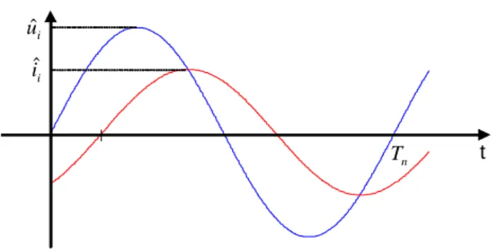
Unbalance in a-b-c phase representation
Compared to what was said in section 2.1.1, unbalance or asymmetry in
phase representation is characterized by phasors
withdifferent peak values
and/or phase distributions different from
120 . An example of unbalanced
°phase voltages and phasors is shown in fig. 2.1-7. Compare with fig 2.1-1.
Figure 2.1-7. Phase voltages (left) and phasor diagram (right) of a three-phase unsymmetrical system.
Unbalance in sequence representation
According to section 2.1.2, unbalance or asymmetry will in sequence
representation lead to the appearance of negative and/or zero sequences.
As an example the phase voltages in fig. 2.1-7 can be split up in a positive, a
negative and a zero sequence according to fig. 2.1-8.
Figure 2.1-8. Visualization of decomposition in sequences.
Unbalance in
α
-β
-γ
-coordinate vector representationDuring balanced conditions, the vector described in section 2.1.4, will rotate circularly on the
α
-β
plane. No movement will appear in theγ
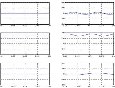
-direction. Fig. 2.1-9a shows the vector trajectory during balanced conditions. Compare it with the sequence representation, where only the positive sequence exists.During unbalanced conditions however, if there is a negative sequence, the backwards rotating negative sequence component will be added to the vector as well. The vector will then consist of two components: One part rotating with the fundamental frequency in the positive direction and one superimposed part rotating
0.06 0.065 0.07 0.075 0.08 -300 -200 -100 0 100 200 300 Phase voltages va vb vc a
v
bv
cv
0.06 0.07 0.08 -300 -200 -100 0 100 200 300 0.06 0.07 0.08 -300 -200 -100 0 100 200 300 0.06 0.07 0.08 -300 -200 -100 0 100 200 300Positive sequence Negative sequence Zero sequence
vap vbp vcp
with the fundamental frequency in the negative direction. This will result in an ellipsoidal vector trajectory on the
α
-β
plane. If there is a zero sequencecomponent, this will appear as a movement with the fundamental frequency in the
γ
-direction. Fig 2.1-9b shows the vector trajectory during unbalanced conditions, assuming that positive, negative, and zero sequences exist. Compare it with the sequence representation during unbalance.Figure 2.1-9a. Vector trajectory in the stationary coordinate system during balanced
conditions.
Figure 2.1-9b. Vector trajectory in the stationary coordinate system during
unbalanced condition
Unbalance in
d-q-o-coordinate vector representationAs mentioned in section 2.1.5, the d-q-0-transformation can be regarded as an observation of the rotating vector from a coordinate system that rotates with the same frequency as the fundamental frequency of the vector in the
α
-β
plane. The d and q axis rotate on theα
-β
plane, while the o axis essentially is the preservedγ
axis. Thus, unbalance leads to the following behavior of the d-,q- and 0-components of a vector in the d-q-0-coordinate system (see fig 2.1-10b).Figure 2.1-10a. Behavior of the d- q- and 0-components of a vector in the
d-q-0-coordinate system during balanced conditions.
Figure 2.1-10b. Behavior of the d- q- and 0-components of a vector in the d-q-0-coordinate system during unbalanced
conditions.
Since the added negative sequence causes an ellipsoidal vector trajectory on the
α
-β
plane, both d and q will have a sinusoidal component, at twice the fundamental frequency, added to their stationary DC components.The zero sequence component will in the 0-direction, as in the
γ
-direction, appear as a sinusoidal component at the fundamental frequency.Definition of unbalance
There are different ways to define unbalanced loads. One way is based on the differences between the maximum per phase load and the minimum per phase load [9]:
100
_
_
_
)
_
_
(
)
_
_
(
%
=
−
⋅
load
phase
three
Total
load
phase
per
Min
load
phase
per
Max
UnBal
Equation 2.1.22The drawback of this definition is that no concern is taken of the load power factors. If different phases are connected to loads with different power factors, conditions that very well may have impacts of the converters performance, will not be distinguished [2]. 0.06 0.065 0.07 0.075 0.08 -400 -200 0 200 400 0.06 0.065 0.07 0.075 0.08 -400 -200 0 200 400 0.06 0.065 0.07 0.075 0.08 -400 -200 0 200 400 0.06 0.065 0.07 0.075 0.08 -400 -200 0 200 400 0.06 0.065 0.07 0.075 0.08 -400 -200 0 200 400 0.06 0.065 0.07 0.075 0.08 -400 -200 0 200 400 d q 0
Another way is to base the definition on the sequence representation. According to [2], IEC gives the definition of unbalance in a three phase system as the ratio between the rms values of the negative sequence, or the zero sequence, and the positive sequence.
100
_
_
_
_
_
%
=
⋅
component
sequence
positive
component
sequence
negative
N
UnBal
Equation 2.1.23 and100
_
_
_
_
0
_
%
=
⋅
component
sequence
positive
component
sequence
zero
UnBal
Equation 2.1.24In the next chapter, where different load conditions are discussed, both definitions will be used.
2.2 Loads to evaluate
The ultimate goal is to create a balanced three-phase voltage source that,
independent of the load condition, always provides the correct voltage. Now, this is more of a target to take aim at, than an in practice achievable goal. The presented simulations of the converter will be limited by a number of different load
conditions. To put a limit to the number of experiments, five different load scenarios considered to be reasonable are chosen.
Only resistive and inductive loads, with power factor between 0.2 and 1, are evaluated. Capacitive loads, that are assumed to be rarer, are put on hold for the time being.
Unbalanced loads are assumed to be a common load for the converter and will therefore be carefully examined. The unbalance may be caused by unevenly distributed single-phase loads, or by a combination of single-phase loads and three-phase loads.
The following scenarios of load conditions will be examined and simulated:
Scenario 1
Balanced load with power factor 1 and a step in the load. Starting at low power (approximately no load) and by a step, reach nominal power (50 kVA).
The scenario simulates that the converter starts with no load connected and then is subject to a purely resistive load, corresponding to rated power of the converter.
Ia (current / powerfactor) Ib (current / powerfactor) Ic (current / powerfactor) %unbalance %neg.seq. unbalance %zero.seq. unbalance In (current) Before step: 0 A/ 1 0 A/ 1 0 A/ 1 0 % 0 % 0 % 0 A After step: 72.2 A/ 1 72.2 A/ 1 72.2 A/ 1 0 % 0 % 0 % 0 A
Table 2.2-1. Load scenario 1.
Scenario 2
Balanced load with power factor 0.2 and a step in the load. Starting at low power (approximately no load) and by a step, reach nominal power (50kVA).
The scenario simulates that the converter starts with no load connected and then is subject to a heavily inductive load, corresponding to rated power of the converter. The interesting part here is to see how well the inverter copes under inductive load conditions. Ia (current / powerfactor) Ib (current / powerfactor) Ic (current / powerfactor) %unbalance %neg.seq. unbalance %zero.seq. unbalance In (current) Before step: 0 A/ 0.2 0 A/ 0.2 0 A/ 0.2 0 % 0 % 0 % 0 A After step: 72.2 A/ 0.2 72.2 A/ 0.2 72.2 A/ 0.2 0 % 0 % 0 % 0 A
Table 2.2-2. Load scenario 2.
Scenario 3
Unbalanced load with power factor 0.8. The phase currents Ib and Ic are set equal to
The scenario simulates that a partly inductive single-phase load is connected to phase a. Phase b and c are not connected. The interesting part here is to see how well the converter copes under unbalanced load conditions.
Ia (current (A)/ powerfactor) Ib (current (A)/ powerfactor) Ic (current (A)/ powerfactor) % unbalance % neg.seq. unbalance % zero.seq. unbalance In (current (A)) No step 72.2 A/ 0.8 0 A 0 A 100 % 100 % 100 % 72.2 A
Table 2.2-3. Load scenario 3.
Scenario 4
A combination of one balanced three-phase load and one single-phase load with a step in the three-phase load. Both loads have a power factor of 0.8. Initially the phase currents Ib and Ic are set to
0
.
5
⋅
I
nominaland the phase current Ia is set toInominal. Then, there is a sudden change in the load so that Ib and Ic are set to 0 and Ia
is set to
0
.
5
⋅
I
nominal.The scenario simulates that one partly inductive three-phase load as well as one partly inductive single-phase load at phase a are connected to the converter. Then the three-phase load is disconnected. The interesting part here is to see how the removal of a quite heavy three-phase load affects the voltage over a simultaneously connected single-phase load.
Ia (current (A)/ powerfactor) Ib (current (A)/ powerfactor) Ic (current (A)/ powerfactor) % unbalance % neg.seq. unbalance % zero.seq. unbalance In (current (A)) Before step: 72.2 A/ 0.8 36.1 A/ 0.8 36.1 A/ 0.8 25 % 25 % 25 % 36.1 A After step: 36.1 A/ 0.8 0 A 0 A 100 % 100 % 100 % 36.1 A
Table 2.2-4. Load scenario 4.
Scenario 5
A combination of one heavily inductive single-phase load and one resistive
single-phase load. The inductive phase chas a power factor of 0.2. Ia and Ic are both
set equal to nominal current Inominal.
The scenario simulates that one heavily inductive single-phase load, as well as one purely resistive single-phase load are connected to the converter. The interesting
part here is to see how the converter behaves under this heavily unbalanced load where the neutral current exceeds the line currents.
Ia (current (A)/ powerfactor) Ib (current (A)/ powerfactor) Ic (current (A)/ powerfactor) % unbalance % neg.seq. unbalance % zero.seq. unbalance In (current (A)) No step: 72.2 A/ 1 0 A 72.2 A/ 0.2 50 % 20 % 120 % 134 A
Table 2.2-5. Load scenario 5.
2.3 Three leg converters
This section deals with the basic theory of three leg power electronic converters. For this project, as will be shown later, the choice has fallen on the use of a four leg converter. Though, for a start, the three leg converter is examined to demonstrate theory, function and properties of three phase converters.
2.3.1 The three leg bridge
The principles for the physical layout of three phase converters, also known as voltage-source converters (VSC:s) are shown in fig. 2.3-1. The bridge is connected to the DC-link, whose voltage is raw material in the creation of the three-phase output voltage. The link voltage is from now on called dc-link. The mid potential of the dc-link is defined as neutral.
Figure 2.3-1.Three-phase converter network.
Between the two poles of the dc link, the three half-bridges are connected. Each half-bridge has two power electronic switches. By switching them, between fully conducting and fully blocking, the potentials of each half-bridge
(v
a, v
b, v
c),
withrespect to the mid potential of the dc link,
can attain
±
V
DC/
2
.
The switch states are denoted (a, b, c). With, for example the state (a, b, c ) = (+,-,-) (like in fig. 2.3-2 a) va =
V
DC/
2
and vb = vc= -V
DC/
2
.LOAD 2 DC V a
v
v
b cv
2 DC V 2 DC V −If the potentials (va, vb, vc) =(
V
DC/
2
, -V
DC/
2
, -V
DC/
2
), like in the exampleabove, are transformed to a vector in
α
-β
-coordinates (according to eq. 2.1.13), it will attain the value:3
2
V
DCv
α=
⋅
,v
β=
0
(as in fig. 2.3-2 b)The switch state (a, b, c) can attain the states (+,-,-), (+,+,-), (-,+,-), (-,+,+), (-,-,+) and (+,-,+), who are creating the six possible active values of the voltage vector, and (+,+,+) and (-,-,-), who are creating the zero-vectors, in the
α
-β
-coordinates according to fig. 2.3-2b.According to eq. 2.1.13, the output voltage vector v in the
α
-β
-plane can therefore only attain the following values:
±
=
±
±
⋅
=
3
,
0
3
2
,
3
,
0
DC DC DCV
v
V
V
v
β α Equation2.3.1The maximum modulus of the voltage vector is:
3
2
V
DCv
=
⋅
Equation2.3.2The resulting vector diagram is shown in fig. 2.3-2b.
Figure 2.3-2a. The three phase converter
switching network. Figure 2.3-2b. The attainable voltage vectors.
DC V 3 2 (-,+,-) (+,+,-) (+,-,-) (+,-,+) (-,-,+) (-,+,+) (-,-,-) (+,+,+)
α
LOAD 2 DC V 2 DC V − av
bv
cv
β
By combining the eight possible switching states, including the zero vectors, using
pulse width modulation (described below), any voltage vector within the hexagon in fig. 2.3-2b can be generated in average. However, there is an even tighter limitation for the voltage vector to achieve a linear modulation, namely the circle that touches the inner sides of the hexagon. The circle has a radius of
3
2
times the maximum modulus of the voltage vector.Circle radius = Vbase =
v
max⋅
3
2
=
V
DC3
Equation 2.3.3The radius of the circle is denoted Vbase which is further referred to in the section
below. vref is the desired value of the mean voltage vector.
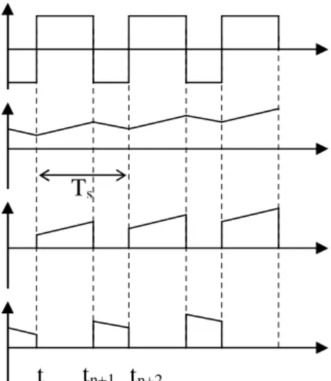
2.3.2 Pulse-width modulation
Pulse-width modulation is a way of choosing the sequence of the switch-states above so that the mean valuevmean, becomes the desired vref. Referring to fig. 2.3-3
the average value can be expressed as:
(
)
[
base base]
mean
t
V
t
V
T
v
=
1
+⋅
+
−⋅
−
Equation 2.3.4Where T is the switch-period and t+ and t- are the periods when the switches, in the
current half bridge, are connecting the phase to Vbase or -Vbase respectively. For
example: If t+ = T, then vmean= Vbase; if t+ = t- = T/2, then vmean = 0 and if t+ = 0, vmean
= -Vbase. The resulting voltage waveform is pulse-width modulated and this
operation of the inverter is called pulse-width modulation (PWM). See fig. 2.3-3.
Figure 2.3-3. Pulse-width modulated waveform and mean value.
The classical method to generate appropriate switching signals from the reference signal v , is the triangle wave comparison method. The idea is to compare v to a
t v base V −
t
−t
+ base Vtriangular carrier signal of amplitude Vbase. When vrefis larger than the carrier, the
potential of the current half-bridge is set to Vbase, and otherwise to
-Vbase. This is illustrated in fig. 2.3-4. The only difference compared to fig. 2.3-3 is
that the switchings are made within the period 0 < t < T and not at the beginning and end of the period.
Figure 2.3-4.Triangle comparison method.
As mentioned above, Vbase was originally set to
V
base=
V
DC3
to achieve a linearmodulation. It is proven to be an unreachable voltage with a sinusoidal reference voltage, since only the potentials
±
V
DC/
2
are available for the potentials delivered from each half-bridge, with respect to the dc-link defined neutral. But, if Vbaseinstead is selected to VDC/2, it is not possible to utilize all of the available dc link
voltage, as shown below.
Since the line to line voltage is equal to the line to neutral voltage times
3
, (U
ab=
U
an⋅
3
), the maximum line to line voltage from the converter will be (see fig. 6a, b, c): DC DC DC phase phaseV
V
V
U
−=
⋅
3
=
⋅
3
2
≈
0
.
87
⋅
2
max_ Equation 2.3.5Since the converter, as later will be seen, will need to deliver as much voltage as possible, this is a drawback.
t v base
V
−
+t
refV
T/2 t v baseV
baseV
−
2
−t
T2
−t
baseV
Figure 2.3-5a. Phase reference potential and line to line reference voltage, compared to
available dc link voltage when Vbase=VDC sq./sq.root(3)
Figure 2.3-5b. Phase reference potential and line to line reference voltage, compared to
available dc link voltage when Vbase=VDC /2.
Figure 2.3-5c. Vbase =VDC / 2 and Vbase =VDC / sq.root(3)
A way to achieve full utilization of the dc link voltage, and still have a linear modulation, is to allow some movements of the neutral point. This method is called
the Symmetrized triangle wave comparison method.
3
DCV
2
DCV
β V 0 0.01 0.02 0.03 0.04 -500 0 500 0 0.01 0.02 0.03 0.04 -500 0 500 0 0.01 0.02 0.03 0.04 -500 0 500 0 0.01 0.02 0.03 0.04 -500 0 500 Line to line reference voltagePhase reference potential
Line to line reference voltage Phase reference potential V DC/2 -V DC/2 V DC V DC α
V
2.3.3 Symmetrized modulation
If the same deviation is added or subtracted from all reference signals (va, vb, vc), a
zero-sequence
∆
is added. The voltage vector v in theα
-β
-plane is by that not altered.By studying the three sinusoidal phase potential waves as a group, one can see that they are moving in an “unsymmetrical way” compared to the center of the
triangular wave. For example, when va reaches its maximum value, vb and vc are at
half of their minimum values (See fig. 2.3-6a).
The key to extend the modulation range is to select
∆
so that:)
'
,
'
,
'
min(
)
'
,
'
,
'
max(
v
av
bv
c=
−
v
av
bv
c . Equation 2.3.6This implies selecting:
2
)
,
,
min(
)
,
,
max(
v
av
bv
c+
v
av
bv
c=
∆
Equation 2.3.7 and∆
−
=
(
,
,
)
)
'
,
'
,
'
(
v
av
bv
cv
av
bv
c Equation 2.3.8Figure 2.3-6a.Sinusoidal modulation. Phase and neutral reference potentials.
Figure 2.3-6b. Symmetrized modulation. Phase reference potentials and zero sequence
deviation (delta).
By doing this, one can see that the amplitude of the symmetrized phase potential references (fig. 2.3-6b), compared to the center of the triangular wave, is less than in the sinusoidal case (2.3-6a). This makes it possible to increase the amplitude of
the line to neutral reference voltage by a factor
2
3
and to select3
DC
base
V
V
=
, still using the maximum phase potentials±
V
DC2
.Since the line to line voltage is
U
ab=
3
⋅
U
an, the maximum line to line voltage will by this method reach3
⋅
V
DC3
=
V
DC, and all of the dc link voltage may be utilized:DC phase
phase
V
U
max_ −=
Equation 2.3.9The line to line voltages will not be affected by the movements in the
neutral point. Only the phase potentials and the potential of the neutral,
with
respect to the dc link defined neutral point
, is altered.
2.3.4 Overmodulation
Using the symmetrized modulation method it is possible, under linear modulation, to reach VDC as the maximum line to line voltage amplitude and
V
DC3
as themaximum line to neutral voltage amplitude. The limit for reachable output voltages
0 0.005 0.01 0.015 0.02 -500 0 500 0 0.005 0.01 0.015 0.02 -500 0 500
Sinusoidal modulation Symmetrized modulation
VDC/2
is thereby set by the dc link. If the reference voltage vector vref reaches outside the
limit set by the circle radius =
V
DC3
inside the hexagon in fig. 2.3-7a, the PWM goes into overmodulation. Then the output voltage vector will follow the reference vector when the reference vector is inside the hexagon and the hexagon when the reference vector is outside the hexagon (fig. 8b).In the following simulations, this will be avoided by limiting the
reference
signal to the linear modulation area:3
DC base refV
V
v
≤
=
Equation 2.3.10Figure 2.3-7a. Limit for overmodulation. Figure 2.3-7b Output voltage during
overmodulation.
2.3.5 Unbalanced conditions
According to the assumption that the load connected to the converter is balanced, the reference voltage vector will follow a circular trajectory in the
α
-β
-plane. The definition in eq. 2.3.10 for the dc link voltage may then be sufficient for control (see fig. 2.3-8a).During balanced load conditions, the reference voltage vector will only consist of the positive sequence component (mentioned earlier in section 2.1.6). During unbalanced load however, a negative sequence component will be added to the reference voltage vector as well. This combination of positive and negative sequence voltages will give the trajectory of the reference voltage vector the shape
α V base V β V Vβ α V
voltage as well as the positive, the major radius of the ellipse must be confined within the inscribed circle of the hexagon, with the radius Vbase.
3
. _ . _ DC base seq neg ref seq pos refV
V
v
v
+
≤
=
Equation 2.3.11The minimum dc link voltage in the unbalanced case depends on the degree of unbalance of the load. However, a higher dc link voltage will lead to a higher ability of the converter to control the output voltage. This may be even more important if the load is unbalanced.
Figure 2.3-8a.Voltage reference vector trajectory under balanced conditions.
Figure 2.3-8b.Voltage reference vector trajectory under unbalanced conditions.
2.3.6 The creation of a neutral connection
For a three-phase three-wire system, due to the topology, the sum of the three phase currents are zero and the voltage in the neutral point is floating. During balanced load condition this is not a problem. Since the potential in the neutral point during balance always will be zero, the load voltages can be correctly controlled. During unbalanced load conditions however, the line to neutral output voltages will unavoidable become unbalanced as well since the voltage in the neutral point cannot be controlled separately.The control target of balanced three-phase voltages contradicts with the fact that the zero-sequence current cannot exist [2].
Only the positive and negative sequence current exists in the system.
In order to make the control target possible, a neutral conductor must be provided so that the zero sequence current can flow through. For a three-phase four-wire system there is a neutral connection that provides current to flow from the neutral point of the load. Here the sum of the three phase currents and the neutral current
β
α
DC V 3 2 DC V 3 2α
βare zero and the voltage in the neutral point may be defined. In this system both positive, negative and zero sequence exists.
Passive methods
There are passive methods to provide the neutral connection for unbalanced loads [2]:
Transformer
The
∆
Υ
transformer is a zero sequence trap. Connecting the∆
windings to the inverter and the Y windings to the load, the zero sequence current caused by the load is trapped into the∆
windings. Circulating within the transformer winding, it is prevented from traveling back to the inverter and the dc link. Another passive way to provide the neutral connection is to use a zig-zag transformer, which also balances the load to some extent. The zero sequence currents from each phase are shifted at different phase angles, and thus can be canceled with each other.The problem with the approaches mentioned above, is that they add the transformer to the converter. Transformers for high power are very bulky components.
Split dc link capacitor
Another passive approach to provide a neutral connection is to use two capacitors to split the dc link and connect the neutral point to the mid-point of the two capacitors (see fig. 2.3-9).
Figure 2.3-9. Split dc link capacitor to provide the neutral point.
There are two problems with this approach. Firstly, the neutral point will be fixed to the middle of the dc link, which will cause poor utilization of the dc link voltage. (The motivation for this is in section 2.3.2, eq. 2.3.5.) Secondly, a huge increase of the capacitance is needed to maintain the dc link voltage ripple at a reasonable level
2 DC V − 1 Z a
v
v
b cv
2 DC V 2 Z 3 ZThe ripple will consist of two frequencies,
2
ω
andω
. The2
ω
ripple is caused by the negative sequence load current and theω
ripple is caused by the zero sequence load current. The ripple caused by the negative sequence current will occur under unbalanced conditions in any case. The ripple caused by the zero sequence current on the other hand, is directly caused by the connection of the neutral conductor to the split dc link capacitor. See Appendix A for calculations of capacitor size.A fourth leg
By replacing the three leg switching network in fig. 2.3-1 with a four leg switching network, as shown in fig. X10, a four half-bridge power electronic converter is obtained. By tying the neutral connection of the load to the mid point of the fourth half-bridge, the four-legged PWM converter can handle the neutral current caused by an unbalanced load. A balanced output voltage can be achieved with a tightly regulated neutral point.
The method should, compared to the above mentioned approaches, have the advantages of:
1. Possibility for high utilization of the dc link voltage. 2. No bulky transformers / much smaller dc link capacitors.
Disadvantages are that one more switch pair and one more output filter inductor are added to the design.
This approach seems to be the most preferable and is the one chosen for the project. From now on, when a converter is mentioned, it refers to a four leg converter if nothing else is mentioned.
2.4 The four legged converter
The choice is made to use a converter with a fourth half-bridge to obtain the neutral connection. This converter has much in common with the regular three-phase converter. With the fourth half-bridge, the possibility to connect the neutral is achieved as well. By this a third degree of freedom is added. Instead of using the
α
-β
coordinates, one have to add yet another dimension and work in theα
-β
2.4.1 The four leg bridge
The layout of a four legged three phase converter is shown in fig. 2.4-1.
Figure 2.4-1. Four-legged converter network.
Each half-bridge has two power electronic switches. By switching them between fully conducting and fully blocking, the potentials of each half-bridge
(v
a, v
b, v
c,v
n)
can all attain
±
V
DC/
2
,
with respect to the neutral point defined as the midpotential of the dc link
. This means that the voltages (v
an, v
bn, v
cn), can
attain
±
V
DC.
The switch states are now denoted (a, b, c, n), (see fig. 2.4-2). Compared to the 8 switch states in the three half-bridge case, the converter with four half-bridges can attain 16 switch states. Since a third degree of freedom is added with the neutral half-bridge and its possibility of a neutral current, the
α
-β
-coordinate system needs an extension to theα
-β
-γ
-coordinate system.If the output voltage components (van, vbn, vcn), according to the 16 possible switch
states of (a, b, c, n), are transformed (using eq. 2.1.17) into a output voltage vector
v in the
α
-β
-γ
-coordinates, it can attain the following values:
±
±
⋅
=
±
=
±
±
⋅
=
3
2
,
3
,
0
3
,
0
3
2
,
3
,
0
DC DC DC DC DCV
V
v
V
v
V
V
v
γ β α Equation 2.4.1 2 DC V ov
v
av
b cv
1 Z Z2 Z3 2 DC V −The resulting vector diagram containing all attainable vectors is shown in fig. 2.4-3.
Figure 2.4-2.The four legged converter switching network.
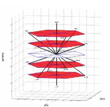
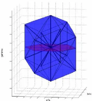
Figure 2.4-3. The output voltage vectors in alfa-beta-gamma coordinates.
By combining the 16 possible switching states, using pulse width modulation, any voltage vector within the polygon in fig. 2.4-4 can be generated in average. Compare this with the hexagon in the three half-bridge converter case.
2 DC V a
v
bv
cv
ov
1 Z Z2 Z3 2 DC V −Figure 2.4-4. The polygon limiting the output voltage vector (reference voltage vector) in the four leg converter case.
2.4.2 Over modulation
The phenomenon is similar to the case with a three leg converter. If the reference voltage vector vref reaches outside the limit set by the polygon in fig.
2.4-4, the PWM goes into overmodulation. The output voltage vector will then follow the reference vector when the reference vector is inside the polygon and the surface of the polygon when the reference vector is outside the sphere.
2.4.3 Unbalanced conditions
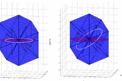
During balanced load conditions, the reference voltage will only consist of the positive sequence component (mentioned earlier in 2.1.6). It will therefore follow a circular trajectory in the
α
-β
-plane (see fig. 2.4-5a).During unbalanced load however, the reference voltage will not only consist of the positive sequence component, but both negative and zero sequence
components may be added as well. The combination of positive, negative and zero sequence voltages will give the trajectory of the reference voltage vector the shape of a skewed ellipse (see fig. 2.4-5b).
Figure 2.4-5a. The reference voltage vector trajectory during balance and the polygon limiting the reference voltage vector in the
four leg converter case.
Figure 2.4-5b.The r