Digital Accelerometer
Preliminary Technical Data
ADXL345
Rev. PrA
Information furnished by Analog Devices is believed to be accurate and reliable. However, no responsibility is assumed by Analog Devices for its use, nor for any infringements of patents or other rights of third parties that may result from its use. Specifications subject to change without notice. No license is granted by implication or otherwise under any patent or patent rights of Analog Devices. Trademarks and registered trademarks are the property of their respective owners.
One Technology Way, P.O. Box 9106, Norwood, MA 02062-9106, U.S.A.
Tel: 781.329.4700 www.analog.com
Fax: 781.461.3113 ©2008 Analog Devices, Inc. All rights reserved.
FEATURES
Ultra low power: 25 to 130 µA at VS = 2.5 V (typ)
Power consumption scales automatically with bandwidth User selectable fixed 10-bit resolution or 4mg/LSB scale
factor in all g-ranges, up to 13-bit resolution at ±16 g 32 level output data FIFO minimizes host processor load Built in motion detection functions
• Tap/Double Tap detection
• Activity/Inactivity monitoring
• Free-Fall detection
Supply and I/O voltage range: 1.8 V to 3.6 V SPI (3 and 4 wire) and I2C digital interfaces
Flexible interrupt modes – Any interrupt mappable to either interrupt pin
Measurement ranges selectable via serial command Bandwidth selectable via serial command
Wide temperature range (-40 to +85°C) 10,000 g shock survival
Pb free/RoHS compliant
Small and thin: 3 × 5 × 1 mm LGA package
APPLICATIONS
Handsets
Gaming and pointing devices Personal navigation devices HDD protection
Fitness equipment Digital cameras
GENERAL DESCRIPTION
The ADXL345 is a small, thin, low power, three-axis
accelerometer with high resolution (13-bit) measurement up to ±16 g. Digital output data is formatted as 16-bit twos
complement and is accessible through either a SPI (3- or 4-wire) or I2C digital interface.
The ADXL345 is well suited for mobile device applications. It measures the static acceleration of gravity in tilt-sensing applications, as well as dynamic acceleration resulting from motion or shock. Its high resolution (4mg/LSB) enables resolution of inclination changes of as little as 0.25°. Several special sensing functions are provided. Activity and inactivity sensing detect the presence or lack of motion and if the acceleration on any axis exceeds a user-set level. Tap sensing detects single and double taps. Free-Fall sensing detects if the device is falling. These functions can be mapped to interrupt output pins. An integrated 32 level FIFO can be used to store data to minimize host processor intervention.
Low power modes enable intelligent motion-based power management with threshold sensing and active acceleration measurement at extremely low power dissipation.
The ADXL345 is supplied in a small, thin 3 mm × 5 mm × 1 mm, 14-lead, plastic package.
FUNCTIONAL BLOCK DIAGRAM
Figure 1. ADXL345 Simplified Block Diagram
3 AXIS SENSOR DIGITAL FILTER A /D C O N V E R TE R SENSE ELECTRONICS CONTROL AND INTERRUPT LOGIC SERIAL I/O POWER MANAGEMENT COM CS SCL/SCLK SDO/ALT ADDRESS SDA/SDI/SDIO INT2 VDDI/O Vs INT1 ADXL345 3 AXIS SENSOR DIGITAL FILTER DIGITAL FILTER A /D C O N V E R TE R SENSE ELECTRONICS CONTROL AND INTERRUPT LOGIC CONTROL AND INTERRUPT LOGIC SERIAL I/O SERIAL I/O POWER MANAGEMENT POWER MANAGEMENT COM CS SCL/SCLK SDO/ALT ADDRESS SDA/SDI/SDIO INT2 VDDI/O Vs INT1 ADXL345
TABLE OF CONTENTS
Features ... 1
Applications... 1
General Description ... 1
Functional Block Diagram ... 1
Revision History ... 2
Specifications... 3
Absolute Maximum Ratings... 4
ESD Caution... 4
Pin Configuration and Descriptions... 5
Typical performance characteristics ... 6
Functional Description ... 7 Device Operation ... 7 Power Sequencing ... 7 Power Saving ... 7 Serial Communications ... 9 SPI... 9 I2C... 10 Interrupts... 11 FIFO ... 11 Self Test ... 12 Register Map ... 13 Register Definitions ... 14 Application ... 18
Power Supply Decoupling ... 18
Mechanical Considerations for Mounting... 18
Tap Detection... 18
Threshold ... 19
Link Mode ... 19
Recommended PWB Land Pattern... 20
Recommended Soldering Profile ... 21
Outline Dimensions ... 22
Ordering Guide ... 22
REVISION HISTORY
Rev. PrA | Page 3 of 24
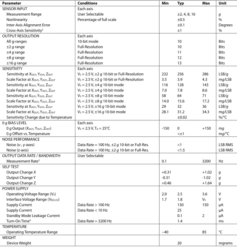
SPECIFICATIONS
TA = 25°C, VS = 2.5 V, VDD I/O = 1.8 V, Acceleration = 0 g, unless otherwise noted.
Table 1. Specifications1
Parameter Conditions Min Typ Max Unit
SENSOR INPUT Each axis
Measurement Range User Selectable ±2, 4, 8, 16 g
Nonlinearity Percentage of full scale ±0.5 % Inter-Axis Alignment Error ±0.1 Degrees
Cross-Axis Sensitivity2 ±1 %
OUTPUT RESOLUTION Each axis
All g-ranges 10-bit mode 10 Bits
±2 g range Full-Resolution 10 Bits ±4 g range Full-Resolution 11 Bits ±8 g range Full-Resolution 12 Bits ±16 g range Full-Resolution 13 Bits SENSITIVITY Each axis
Sensitivity at XOUT, YOUT, ZOUT VS = 2.5 V, ±2 g 10-bit or Full-Resolution 232 256 286 LSB/g
Scale Factor at XOUT, YOUT, ZOUT VS = 2.5 V, ±2 g 10-bit or Full-Resolution 3.5 3.9 4.3 mg/LSB
Sensitivity at XOUT, YOUT, ZOUT VS = 2.5 V, ±4 g 10-bit mode 116 128 143 LSB/g
Scale Factor at XOUT, YOUT, ZOUT VS = 2.5 V, ±4 g 10-bit mode 7.0 7.8 8.6 mg/LSB
Sensitivity at XOUT, YOUT, ZOUT VS = 2.5 V, ±8 g 10-bit mode 58 64 71 LSB/g
Scale Factor at XOUT, YOUT, ZOUT VS = 2.5 V, ±8 g 10-bit mode 14.0 15.6 17.2 mg/LSB
Sensitivity at XOUT, YOUT, ZOUT VS = 2.5 V, ±16 g 10-bit mode 29 32 36 LSB/g
Scale Factor at XOUT, YOUT, ZOUT VS = 2.5 V, ±16 g 10-bit mode 28.1 31.2 34.3 mg/LSB
Sensitivity Change due to Temperature ±0.02 %/°C 0 g BIAS LEVEL Each axis
0 g Output (XOUT, YOUT, ZOUT) VS = 2.5 V, TA = 25°C -150 0 +150 mg
0 g Offset vs. Temperature <±1 mg/°C NOISE PERFORMANCE
Noise (x-, y-axes) Data Rate = 100 Hz, ±2 g 10-bit or Full-Res. <1 LSB RMS Noise (z-axis) Data Rate = 100 Hz, ±2 g 10-bit or Full-Res. <1.5 LSB RMS OUTPUT DATA RATE / BANDWIDTH User Selectable
Measurement Rate3 0.1 3200 Hz SELF TEST Output Change X +0.31 +1.02 g Output Change Y -0.31 -1.02 g Output Change Z +0.46 +1.64 g POWER SUPPLY
Operating Voltage Range (VS) 2.0 2.5 3.6 V
Interface Voltage Range (VDD I/O) 1.7 1.8 VS V
Supply Current Data Rate > 100 Hz 130 150 µA Supply Current Data Rate < 10 Hz 25 µA Standby Mode Leakage Current 0.1 2 µA Turn-On Time4 Data Rate = 3200 Hz 1.4 ms
TEMPERATURE
Operating Temperature Range −40 85 °C WEIGHT
Device Weight 20 mgrams
1 All minimum and maximum specifications are guaranteed. Typical specifications are not guaranteed. 2 Cross-axis sensitivity is defined as coupling between any two axes.
3 Bandwidth is half the output data rate.
4 Turn-on and wake-up times are determined by the user defined bandwidth. At 100 Hz data rate the turn-on/wake-up time is approximately 11.1 ms. For additional data rates the turn-on/wake-up time is approximately τ + 1.1 in milliseconds, where τ is 1/(Data Rate).
ABSOLUTE MAXIMUM RATINGS
Table 2. Absolute Maximum RatingsParameter Rating
Acceleration (Any Axis, Unpowered) 10,000 g
Acceleration (Any Axis, Powered) 10,000 g
VS −0.3 V to 3.6 V
VDD I/O −0.3 V to 3.6
All Other Pins −0.3 V to 3.6 Output Short-Circuit Duration
(Any Pin to Ground)
Indefinite Temperature Range (Powered) −40°C to +105°C Temperature Range (Storage) −40°C to +105°C
Stresses above those listed under Absolute Maximum Ratings may cause permanent damage to the device. This is a stress rating only; functional operation of the device at these or any other conditions above those indicated in the operational section of this specification is not implied. Exposure to absolute maximum rating conditions for extended periods may affect device reliability.
ESD CAUTION
ESD (electrostatic discharge) sensitive device. Electrostatic charges as high as 4000 V readily accumulate on the human body and test equipment and can discharge without detection. Although this product features proprietary ESD protection circuitry, permanent damage may occur on devices subjected to high energy electrostatic discharges. Therefore, proper ESD precautions are recommended to avoid performance degradation or loss of functionality.
Rev. PrA | Page 5 of 24
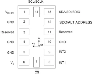
PIN CONFIGURATION AND DESCRIPTIONS
Figure 2. Pin Configuration (Top View) Table 3. Pin Descriptions
Pin No. Mnemonic Description
1 VDD I/O Digital Interface Supply Voltage
2 GND Must be connected to ground
3 Reserved Reserved, must be connected to VS or left open
4 GND Must be connected to ground 5 GND Must be connected to ground 6 VS Supply Voltage
7 CS Chip Select 8 INT1 Interrupt 1 Output 9 INT2 Interrupt 2 Output
10 GND Must be connected to ground
11 Reserved Reserved, must be connected to GND or left open 12 SDO/ALT ADDRESS Serial Data Out, Alternate I2C Address Select
13 SDA/SDI/SDIO Serial Data (I2C), Serial Data In (SPI 4-Wire), Serial Data In/Out (SPI 3-Wire)
14 SCL/SCLK Serial Communications Clock
Rev. PrA | Page 7 of 24
FUNCTIONAL DESCRIPTION
DEVICE OPERATION
The ADXL345 is a complete three-axis acceleration
measurement system with a selectable measurement range of either ±2 g, ±4 g, ±8 g, or ±16 g. It measures both dynamic acceleration resulting from motion or shock and static acceleration, such as gravity, which allows it to be used as a tilt sensor. The sensor is a polysilicon surface-micromachined structure built on top of a silicon wafer. Polysilicon springs suspend the structure over the surface of the wafer and provide a resistance against acceleration forces. Deflection of the structure is measured using differential capacitors that consist of independent fixed plates and plates attached to the moving mass. Acceleration deflects the beam and unbalances the differential capacitor, resulting in a sensor output whose amplitude is proportional to acceleration. Phase-sensitive demodulation is used to determine the magnitude and polarity of the acceleration.
POWER SEQUENCING
Power may be applied to VS or VDD I/O in any sequence without
damaging the ADXL345. All possible power on states are summarized in Table 4. The interface voltage level is set with the interface supply voltage VDD I/O, which must be present to
ensure that the ADXL345 does not create a conflict on the communications bus. For single-supply operation, VDD I/O can be
the same as the main supply, VS. Conversely, in a dual-supply
application, VDD I/O can differ from VS to accommodate the
desired interface voltage. Once VS is applied, the device enters
standby state, where power consumption is minimized and the device waits for VDD I/O to be applied and a command to enter
measurement state (setting the MEASURE bit in the
POWER_CTL register). Clearing the MEASURE bit returns the device to standby state.
Table 4. Power Sequencing
Condition VS VDD I/O Description
Power Off Off Off Completely off, potential for communications bus conflict.
Bus Enabled Off On No functions available, but will not create conflict on communications bus.
Standby or
Measurement On On
At power up the device is in Standby mode awaiting a command to enter measurement mode and all sensor functions are off. Once instructed to enter Measurement mode, all sensor functions are available.
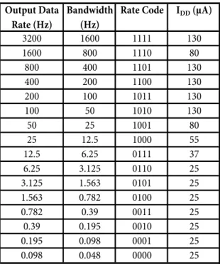
POWER SAVING
Power ModesThe ADXL345 automatically modulates its power consumption proportionally with its output data rate as shown in Table 5. If
additional power savings is desired, a lower power mode is available. In this mode, the internal sampling rate is reduced allowing for power savings in the 12.5 to 400Hz data rate range at the expense of slightly greater noise. To enter lower power mode, set the LOW_POWER bit(D4) in the BW_RATE register.
Table 5. Current Consumption versus Data Rate
Output Data Rate (Hz)
Bandwidth (Hz)
Rate Code IDD (µA)
3200 1600 1111 130 1600 800 1110 80 800 400 1101 130 400 200 1100 130 200 100 1011 130 100 50 1010 130 50 25 1001 80 25 12.5 1000 55 12.5 6.25 0111 37 6.25 3.125 0110 25 3.125 1.563 0101 25 1.563 0.782 0100 25 0.782 0.39 0011 25 0.39 0.195 0010 25 0.195 0.098 0001 25 0.098 0.048 0000 25
The current consumption in Low Power Mode is shown in Table 6. Cases where there is no advantage to using Low Power Mode are shaded.
Table 6. Current Consumption versus Data Rate in Low Power Mode
Output Data Rate
Bandwidth (Hz)
Rate Code IDD (µA)
3200 1600 1111 130 1600 800 1110 80 800 400 1101 130 400 200 1100 80 200 100 1011 55 100 50 1010 37 50 25 1001 30 25 12.5 1000 25 12.5 6.25 0111 25 6.25 3.125 0110 25 3.125 1.563 0101 25 1.563 0.782 0100 25 0.782 0.39 0011 25 0.39 0.195 0010 25 0.195 0.098 0001 25 0.098 0.048 0000 25
Auto Sleep Mode
Additional power can be saved by having the ADXL345 automatically switch to sleep mode during periods of inactivity. To enable this feature set the THRESH_INACT register to an acceleration value that signifies no activity (this value will depend on the application), set TIME_INACT to an appropriate inactivity time period (again, this will depend on the application), and set the AUTO_SLEEP bit and the LINK bit in the POWER_CTL register. Current consumption at the sub-8Hz data rates used in this mode is typically 25 µA.
Standby Mode
For even lower power operation Standby Mode can be used. In Standby Mode current consumption is reduced to 2µA (typical). In this mode no measurements are made and communication with the ADXL345 is limited to single-byte read or writes. Standby Mode is entered by clearing the MEASURE bit (D3) in the POWER_CTL register. Placing the device into Standby Mode will preserve the contents of the FIFO.
Rev. PrA | Page 9 of 24
SERIAL COMMUNICATIONS
I2C and SPI digital communications are available. In both cases,
the ADXL345 operates as a slave. I2C mode is enabled if the CS
pin is tied high to VDD I/O. In SPI mode, the CS pin is controlled
by the bus master. In both SPI and I2C modes of operation, data
transmitted from the ADXL345 to the master device should be ignored during writes to the ADXL345.
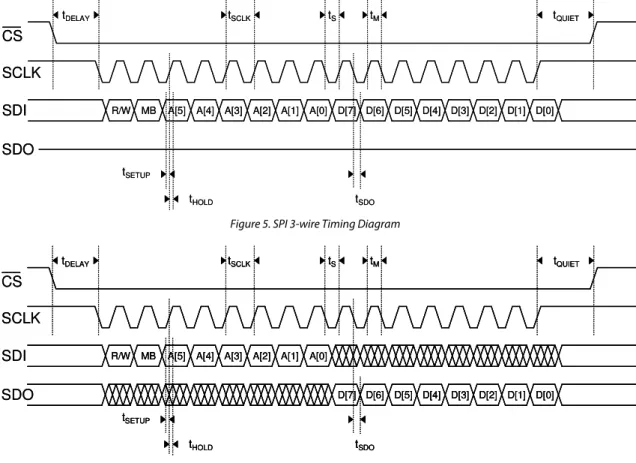
SPI
For SPI, either 3-wire or 4-wire configuration is possible, as shown in the connection diagrams in Figure 3 and Figure 4. Clearing the SPI bit in the DATA_FORMAT register selects 4-wire mode while setting the SPI bit selects 3-wire mode. The maximum SPI clock speed is 5 MHz, with 12 pF maximum loading and the timing scheme follows CPOL = 1, CPHA = 1.
Figure 3. 4-Wire SPI connection
CS is the serial port enable line, and is controlled by the SPI master. It must go low at the start of transmissions and back
Figure 4. 3-Wire SPI connection
high at the end as shown in Figure 5. SCLK is the serial port clock and is supplied by the SPI master. It is stopped high when CS is high, during period of no transmission. SDI and SDO are the serial data in and out respectively. Data should be sampled at the rising edge of SCLK.
To read or write multiple bytes in a single transmission, the Multi-Byte bit, located after the R/W bit in the first byte transfer, must be set. After the register addressing and the first byte of data, continued clock pulses will cause the ADXL345 to point to the next register for read or write. Continued clock pulses will continue to shift the register that is pointed to until the clock pulses are ceased and CS is de-asserted. To perform reads or writes on different, non-sequential registers, CS must be de-asserted between transmissions and the new register must be addressed separately.
The timing diagram for 3-wire SPI reads or writes is shown in Figure 5. The 4-wire equivalents for SPI reads and writes are shown in Figure 6 and Figure 7 respectively.
CS SCLK SDI SDO
R/W MB A[5] A[4] A[3] A[2] A[1] A[0] D[7] D[6] D[5] D[4] D[3] D[2] D[1] D[0]
tDELAY tSCLK tS tM tQUIET tSETUP tHOLD tSDO CS SCLK SDI SDO
R/W MB A[5] A[4] A[3] A[2] A[1] A[0] D[7] D[6] D[5] D[4] D[3] D[2] D[1] D[0]
tDELAY tSCLK tS tM tQUIET
tSETUP
tHOLD tSDO
Figure 5. SPI 3-wire Timing Diagram
CS SCLK SDI SDO
R/W MB A[5] A[4] A[3] A[2] A[1] A[0]
D[6] D[7] D[5] D[4] D[3] D[2] D[1] D[0] tDELAY tSCLK tS tM tQUIET tSETUP tHOLD tSDO CS SCLK SDI SDO
R/W MB A[5] A[4] A[3] A[2] A[1] A[0]
D[6]
D[7] D[5] D[4] D[3] D[2] D[1] D[0]
tDELAY tSCLK tS tM tQUIET
tSETUP
tHOLD tSDO
R/W MB A[5] A[4] A[3] A[2] A[1] A[0]
D[6]
D[7] D[5] D[4] D[3] D[2] D[1] D[0]
tDELAY tSCLK tS tM tQUIET
tSETUP
tHOLD tSDO
Figure 6. SPI 4-wire Read Timing Diagram
ADXL345 PROCESSOR CS D OUT SDA/SDI/SDIO D IN/OUT SDO SCL/SCLK D OUT ADXL345 PROCESSOR D OUT SDA/SDI/SDIO D IN/OUT SDO D IN SCL/SCLK D OUT CS
CS SCLK SDI SDO
R/W MB A[5] A[4] A[3] A[2] A[1] A[0] D[7] D[6] D[5] D[4] D[3] D[2] D[1] D[0]
tDELAY tSCLK tS tM tQUIET tSETUP tHOLD tSDO CS SCLK SDI SDO
R/W MB A[5] A[4] A[3] A[2] A[1] A[0] D[7] D[6] D[5] D[4] D[3] D[2] D[1] D[0]
tDELAY tSCLK tS tM tQUIET
tSETUP
tHOLD tSDO
Figure 7. SPI 4-wire Write Timing Diagram
Table 7. SPI Timing Specifications (TA = 25°C, VS = 2.5V, VDD I/O = 1.8V)
Parameter Limit Unit Description
fSCLK 5 MHz max SPI clock frequency
tSCLK 200 ns min
1/(SPI clock frequency) Mark/space ratio for the SCLK input is 40/60 to 60/40
tDELAY 200 ns min falling edge to SCLK falling edge tQUIET 200 ns min SCLK rising edge to rising edge tS 0.4 × tSCLK ns min SCLK low pulse width (space) tM 0.4 × tSCLK ns min SCLK high pulse width (mark) tSDO 8 ns max SCLK falling edge to SDO transition tSETUP 10 ns min SDI valid before SCLK rising edge tHOLD 10 ns min SDI valid after SCLK rising edge
I
2C
With CS tied high to VDD I/O, the ADXL345 is in I2C mode,
requiring a simple 2-wire connection as shown in Figure 8. The ADXL345 conforms to The I2C Bus Specification, Version 2.1, January 2000, available from Phillips Semiconductor. It supports standard (100 kHz) and fast (400 kHz) data transfer modes. Single or multiple byte read/writes are supported as shown in Figure 9. With the SDO pin high the 7 bit I2C address
for the device is 0x1D, followed by the read/write bit. This translates to 0x3A for write, 0x3B for read. An alternate I2C
address of 0x53 (followed by the read/write bit) may be chosen by grounding the SDO pin (pin 12). This translates to 0xA6 for write, 0xA7 for read.
Figure 8. I2C Connection Diagram (Address = 0x53)
If other devices are connected to the same I2C bus, the nominal
operating voltage level of these other devices cannot exceed VDD I/O by more than 0.3 V. Pull-up resistors, RP, should be in the
range of 1k to 20kΩ.
Master Start Slave Address + Write Register Address
Slave Ack Ack Ack
Master Start Slave Address + Write Register Address
Slave Ack Ack Ack Ack
Master Start Slave Address + Write Register Address Start1 Stop
Slave Ack Ack
Master Start Slave Address + Write Register Address Start1 NAck Stop
Slave Ack Ack
1This Start is either a restart or a Stop followed by a Start
Data Stop
Ack Single Byte Write
Multi-Byte Write
Data
Data
Multi-Byte Read
Slave Address + Read
Slave Address + Read Ack Data Data Data Stop NAck Ack Single Byte Read
Figure 9. I2C Timing Diagram
ADXL345 PROCESSOR CS SDA/SDI/SDIO D IN/OUT SDO SCL/SCLK D OUT RP RP VDD I/O 06238- 007 ADXL345 PROCESSOR CS SDA/SDI/SDIO D IN/OUT SDO SCL/SCLK D OUT RP RP VDD I/O 06238- 007
Rev. PrA | Page 11 of 24
INTERRUPTS
The ADXL345 provides two output pins for driving interrupts: INT1 and INT2. Each of the interrupt functions are described in detail below. All functions can be used simultaneously, with the only limiting feature being that some functions may need to share interrupt pins. Interrupts are enabled by setting the appropriate bit in the INT_ENABLE register and are mapped to either the INT1 or INT2 pins based on the contents of the INT_MAP register. It is recommended that interrupts be configured with the interrupts disabled, preventing interrupts from being accidentally triggered during configuration. This can be done by writing a value of 0x00 to the INT_ENABLE register.
DATA_READY
DATA_READY is set when new data is available and cleared when no new data is available.
SINGLE_TAP
SINGLE_TAP is set when single acceleration event that is greater than the value in the THRESH_TAP register occurs for a time shorter than specified in the DUR register.
DOUBLE_TAP
DOUBLE_TAP is set when two acceleration events that are greater than the value in the THRESH_TAP register occur that are shorter than the time specified in the DUR register, with the second tap starting after the time specified by the LATENT register and within the time specified in the WINDOW register. See the Tap Detection description in the Application section for more details.
ACTIVITY
ACTIVITY is set when acceleration greater than the value stored in THRESH_ACT is experienced.
INACTIVITY
INACTIVITY is set when acceleration of less than the value stored in the THRESH_INACT register is experienced for longer than the time specified in the TIME_INACT register. The maximum value for TIME_INACT is 255 s.
FREE_FALL
FREE_FALL is set when acceleration of less than the value stored in the THRESH_FF register is experienced for longer than the time specified in the TIME_FF register. The FREE_FALL interrupt differs from INACTIVITY interrupt in that all axes always participate, the timer period is much smaller (1.28 s maximum) and it is always DC coupled.
WATERMARK
WATERMARK is set when the FIFO has filled up to the value stored in SAMPLES. It is cleared automatically when the FIFO is read and its content emptied below the value stored in SAMPLES.
OVERRUN
OVERRUN is set when new data has replaced unread data. The precise operation of OVERRUN depends on the FIFO mode. In Bypass Mode, OVERRUN is set when new data replaces unread data in the DATAX, DATAY, and DATAZ registers. In all other modes, OVERRUN is set when the FIFO is filled. OVERRUN is cleared by reading the FIFO contents, and is automatically cleared when the data is read.
FIFO
The ADXL345 contains a 32 level FIFO that can be used to minimize host processor intervention. The FIFO has four modes as described in Table 15 in the Register Definitions section. Mode selection is made by setting the appropriate MODE bits in the FIFO_CTL register. Each FIFO mode is described below.
Bypass Mode
In Bypass Mode the FIFO is not operational and remains empty. FIFO Mode
In FIFO Mode data from X, Y, and Z measurements go into the FIFO. When the FIFO is filled to the level specified in SAMPLES (in the FIFO_CTL register), the WATERMARK interrupt is set. The FIFO will continue filling until it is full (32 X, Y, and Z samples) and then stop collecting data. After the FIFO has stopped collecting data the device still continues to operate, so features like Tap detection, for example, may still be used once the FIFO is full. The WATERMARK interrupt will continue to occur until the number of samples in the FIFO is less than the value of SAMPLES in the FIFO_CTL register. Stream Mode
In Stream Mode data from X, Y, and Z measurements go into the FIFO. When the FIFO is filled to the level specified in SAMPLES (in the FIFO_CTL register), the WATERMARK interrupt is set. The FIFO will continue filling, and will hold the latest 32 X, Y, and Z samples, discarding older data as new data arrives. The WATERMARK interrupt will continue to occur until the number of samples in the FIFO is less than the value of SAMPLES in the FIFO_CTL register.
Trigger Mode
In Trigger Mode, the FIFO fills and holds the latest 32 X, Y, and Z samples. Once a trigger event occurs (as described by the TRIG_SOURCE bit in the FIFO_CTL register), the FIFO will keep the last n samples (where n is the value specified by SAMPLES in the FIFO_CTL register) and then operate in FIFO mode, collecting new samples only when the FIFO is not full. Additional trigger events will not be recognized until Trigger Mode is reset. This can be done by setting the device in Bypass Mode, reading the FIFO_STATUS register and then setting the device back into Trigger Mode. The FIFO data should be read first, as placing the device into Bypass Mode will clear the FIFO.
Retrieving Data from the FIFO
FIFO data is read through the DATAX, DATAY and DATAZ registers. When the FIFO is in FIFO, Stream, or Trigger Modes, reads to the DATAX, DATAY, and DATAZ registers read data stored in the FIFO. Each time any data is read from the FIFO the oldest X, Y, and Z data is placed into the DATAX, DATAY and DATAZ registers. If a single byte read operation is performed, the remaining bytes worth of data will be lost. Therefore, all axes of interest should be read in a burst (or multi-byte) read operation. To ensure that the FIFO has completely popped, there must be at least 5 μs between the end of reading the data registers, signified by the transition to register 0x38 from 0x37 or the CS pin going high, and the start of new reads of the FIFO or reading the FIFO_STATUS register. For SPI operation at 1.5 MHz or lower, the register addressing portion of the transmission is sufficient delay to ensure the FIFO has completely popped. It is necessary for SPI operation greater than 1.5 MHz to de-assert the CS pin to ensure a total of 5 μs, which is at most 3.4 μs at 5 MHz operation. This is not a concern when using I2C, as the
communication rate is low enough to ensure a sufficient delay between FIFO reads.
SELF TEST
The ADXL345 incorporates a Self Test feature that effectively tests both its mechanical and electronic systems. When the Self Test function is enabled (via the SELF_TEST bit in the DATA_FORMAT register), an electrostatic force is exerted on the mechanical sensor. This electrostatic force moves the mechanical sensing element in the same manner as
acceleration, and it is additive to the acceleration experienced by the device. This added electrostatic force results in an output change in the X, Y, and Z-axes. Because the electrostatic force is proportional to VS2, the output change varies with VS.
The Self Test feature on the ADXL345 exhibits a bi-modal behavior which depends upon which phase of the clock Self Test is enabled. Due to this, a typical value for Self Test is not reported; however, the limits shown in Table 1 and below are valid for both potential values.
Table 8. Self Test output in LSB for 2 g and Full-Resolution
Vs = 2.5 V Vs = 3.3 V Min. Typ. Max. Min. Typ. Max. X-Axis +80 +260 +140 +455 Y-Axis -80 -260 -140 -455
Table 9. Self Test output in LSB for 4 g 10-bit
Vs = 2.5 V Vs = 3.3 V Min. Typ. Max. Min. Typ. Max. X-Axis +40 +130 +70 +225 Y-Axis -40 -130 -70 -225 Z-Axis +60 +210 +105 +365
Table 10. Self Test output in LSB for 8 g 10-bit
Vs = 2.5 V Vs = 2.5 V Min. Typ. Max. Min. Typ. Max.
X-Axis +20 +65 +35 +113
Y-Axis -20 -65 -35 -113
Z-Axis +30 +105 +52 +183
Table 11. Self Test output in LSB for 16 g 10-bit
Vs = 2.5 V Vs = 2.5 V Min. Typ. Max. Min. Typ. Max.
X-Axis +10 +33 +17 +57
Y-Axis -10 -33 -17 -57
Rev. PrA | Page 13 of 24
REGISTER MAP
Table 12. Register MapHex Dec Name Type Reset Value Description
0 0 DEVID R 11100101 Device ID.
1 1 Reserved Reserved. Do not access.
to Reserved. Do not access.
1C 28 Reserved Reserved. Do not access.
1D 29 THRESH_TAP R/W 00000000 Tap threshold
1E 30 OFSX R/W 00000000 X axis offset
1F 31 OFSY R/W 00000000 Y axis offset
20 32 OFSZ R/W 00000000 Z axis offset
21 33 DUR R/W 00000000 Tap duration
22 34 LATENT R/W 00000000 Tap latency
23 35 WINDOW R/W 00000000 Tap window
24 36 THRESH_ACT R/W 00000000 Activity threshold
25 37 THRESH_INACT R/W 00000000 Inactivity threshold
26 38 TIME_INACT R/W 00000000 Inactivity time
27 39 ACT_INACT_CTL R/W 00000000 Axis enable control for ACT/INACT
28 40 THRESH_FF R/W 00000000 Free-fall threshold
29 41 TIME_FF R/W 00000000 Free-fall time
2A 42 TAP_AXES R/W 00000000 Axis control for Tap/Double Tap
2B 43 ACT_TAP_STATUS R 00000000 Source of Tap/Double Tap
2C 44 BW_RATE R/W 00001010 Data Rate and Power Mode control
2D 45 POWER_CTL R/W 00000000 Power Save features control
2E 46 INT_ENABLE R/W 00000000 Interrupt enable control
2F 47 INT_MAP R/W 00000000 Interrupt mapping control
30 48 INT_SOURCE R 00000000 Source of interrupts
31 49 DATA_FORMAT R/W 00000000 Data format control
32 50 DATAX0 R 00000000
33 51 DATAX1 R 00000000 X axis data
34 52 DATAY0 R 00000000
35 53 DATAY1 R 00000000 Y axis data
36 54 DATAZ0 R 00000000
37 55 DATAZ1 R 00000000 Z axis data
38 56 FIFO_CTL R 00000000 FIFO control
REGISTER DEFINITIONS
0x00 DEVID (read-only)D7 D6 D5 D4 D3 D2 D1 D0
1 1 1 0 0 1 0 1
DEVID holds a fixed device ID code of 0xE5 (345 octal).
0x1D THRESH_TAP (read/write)
D7 D6 D5 D4 D3 D2 D1 D0
MSB D6 D5 D4 D3 D2 D1 LSB
THRESH_TAP holds the threshold value for tap interrupts. The data format is unsigned, so the magnitude of the tap event is compared to THRESH_TAP. The scale factor is 62.5 mg/LSB (i.e. 0xFF = +16 g). A zero value may result in undesirable behavior if Tap/Double Tap interrupts are enabled.
0x1E, 0x1F, 0x20 OFSX, OFSY, OFSZ (read/write)
D7 D6 D5 D4 D3 D2 D1 D0
MSB D6 D5 D4 D3 D2 D1 LSB
OFSX/OFSY/OFSZ offer user offset adjustments in twos-compliment form with a scale factor of 15.6 mg/LSB (i.e. 0x7F = +2 g).
0x21 DUR (read/write)
D7 D6 D5 D4 D3 D2 D1 D0
MSB D6 D5 D4 D3 D2 D1 LSB
DUR is an unsigned time value representing the maximum time that an event must be above the THRESH_TAP threshold to qualify as a tap event. The scale factor is 625 µs/LSB. A zero value will prevent Tap/Double Tap functions from working.
0x22 LATENT (read/write)
D7 D6 D5 D4 D3 D2 D1 D0
MSB D6 D5 D4 D3 D2 D1 LSB
LATENT is an unsigned time value representing the wait time from the detection of a tap event to the opening of the time window WINDOW for a possible second tap event. The scale factor is 1.25 ms/LSB. A zero value will disable the Double Tap function.
0x23 WINDOW (read/write)
D7 D6 D5 D4 D3 D2 D1 D0
MSB D6 D5 D4 D3 D2 D1 LSB
WINDOW is an unsigned time value representing the amount of time after the expiration of LATENT during which a second tap can begin. The scale factor is 1.25 ms/LSB. A zero value will disable the Double Tap function.
0x24 THRESH_ACT (read/write)
D7 D6 D5 D4 D3 D2 D1 D0
MSB D6 D5 D4 D3 D2 D1 LSB
THRESH_ACT holds the threshold value for activity detection. The data format is unsigned, so the magnitude of the activity event is compared to THRESH_ACT. The scale factor is 62.5 mg/LSB. A zero value may result in undesirable behavior if Activity interrupt is enabled.
0x25 THRESH_INACT (read/write)
D7 D6 D5 D4 D3 D2 D1 D0
MSB D6 D5 D4 D3 D2 D1 LSB
THRESH_INACT holds the threshold value for inactivity detection. The data format is unsigned, so the magnitude of the inactivity event is compared to THRESH_INACT. The scale factor is 62.5 mg/LSB. A zero value may result in undesirable behavior if Inactivity interrupt is enabled.
0x26 TIME_INACT (read/write)
D7 D6 D5 D4 D3 D2 D1 D0
MSB D6 D5 D4 D3 D2 D1 LSB
TIME_INACT is an unsigned time value representing the amount of time that acceleration must be below the value in THRESH_INACT for inactivity to be declared. The scale factor is 1 second/LSB. Unlike the other interrupt functions, which operate on unfiltered data(See Threshold description in Application section), the inactivity function operates on the filtered output data. At least one output sample must be generated for the inactivity interrupt to be triggered. This will result in the function appearing un-responsive if the
TIME_INACT register is set with a value less than the time constant of the Output Data Rate. A zero value will result in an interrupt when the output data is below THRESH_INACT.
Rev. PrA | Page 15 of 24 0x27 ACT_INACT_CONTROL (read/write) D7 D6 D5 D4 D3 D2 D1 D0 ACT AC/DC ACT_X Enable ACT_Y Enable ACT_Z Enable INACT AC/DC INACT_X Enable INACT_Y Enable INACT_Z Enable X/Y/Z Enable: A ‘1’ enables X, Y, or Z participation in activity or inactivity detection. A ‘0’ excludes the selected axis from participation. If all of the axes are excluded, the function is disabled.
AC/DC: A ‘0’ = DC coupled operation and a ‘1’ = AC coupled operation. In DC coupled operation, the current acceleration is compared with THRESH_ACT and THRESH_INACT directly to determine whether activity or inactivity is detected. In AC coupled operation for activity detection, the acceleration value at the start of activity detection is taken as a reference value. New samples of acceleration are then compared to this reference value and if the magnitude of the difference exceeds THRESH_ACT the device will trigger an activity interrupt. In AC coupled operation for inactivity detection, a reference value is used again for comparison and is updated whenever the device exceeds the inactivity threshold. Once the reference value is selected, the device compares the magnitude of the difference between the reference value and the current acceleration with THRESH_INACT. If the difference is below THRESH_INACT for a total of TIME_INACT, the device is considered inactive and the inactivity interrupt is triggered.
0x28 THRESH_FF (read/write)
D7 D6 D5 D4 D3 D2 D1 D0
MSB D6 D5 D4 D3 D2 D1 LSB
THRESH_FF holds the threshold value for Free-Fall detection. The data format is unsigned. The root-sum-square(RSS) value of all axes is calculated and compared to the value in
THRESH_FF to determine if a free fall event may be occurring. The scale factor is 62.5 mg/LSB. A zero value may result in undesirable behavior if Free-Fall interrupt is enabled. Values between 300 and 600 mg (0x05 to 0x09) are recommended.
0x29 TIME_FF (read/write)
D7 D6 D5 D4 D3 D2 D1 D0
MSB D6 D5 D4 D3 D2 D1 LSB
TIME_FF is an unsigned time value representing the minimum time that the RSS value of all axes must be less than
THRESH_FF to generate a Free-Fall interrupt. The scale factor is 5 ms/LSB. A zero value may result in undesirable behavior if Free-Fall interrupt is enabled. Values between 100 to 350 ms (0x14 to 0x46) are recommended.
0x2A TAP_AXES (read/write)
D7 D6 D5 D4 D3 D2 D1 D0 0 0 0 0 SUPPRESS TAP_X Enable TAP_Y Enable TAP_Z Enable TAP_X/Y/Z Enable: A ‘1’ in TAP_X, Y, or Z Enable enables X, Y, or Z participation in Tap detection. A ‘0’ excludes the selected axis from participation in Tap detection.
Setting the SUPPRESS bit suppresses Double Tap detection if acceleration greater than THRESH_TAP is present between taps. See Tap Detection in the Application Section for more details. 0x2B ACT_TAP_STATUS (read) D7 D6 D5 D4 D3 D2 D1 D0 X ACT_X Source ACT_Y Source ACT_Z Source ASLEEP TAP_X Source TAP_Y Source TAP_Z Source X/Y/Z Source: Indicate the first axis involved in a Tap or Activity event. A ‘1’ corresponds to involvement in the event and a ‘0’ corresponds to no involvement. They are not cleared, but overwritten by new data. ACT_TAP_STATUS should be read before clearing the interrupt. Disabling an axis from participation will clear the corresponding Source bit when the next Activity or Tap/Double Tap event occurs.
ASLEEP: A ‘1’ indicates that the part is in the Auto Sleep Mode. A ‘0’ indicates that the part is not using Auto Sleep Mode. See the POWER_CTL description for more information on Auto Sleep Mode.
0x2C BW_RATE (read/write)
D7 D6 D5 D4 D3 D2 D1 D0
X X X LOW_POWER RATE
LOW_POWER: A ‘0’ = Normal operation and a ‘1’ = Reduced power operation with somewhat higher noise. (See Power Modes section for details).
RATE: Selects device bandwidth and output data rate. See Table 5 and Table 6 for details. Default value is 0x0A, or 100 Hz Output Data Rate. An Output Data Rate should be selected that is appropriate for the communication protocol and frequency selected. Selecting too high of an Output Data Rate with a low communication speed will result in samples being discarded.
0x2D POWER_CTL (read/write)
D7 D6 D5 D4 D3 D2 D1 D0
X X LINK AUTO_SLEEP MEASURE SLEEP WAKEUP
LINK: A ‘1’ with both the activity and inactivity functions enabled will delay the start of the activity function until inactivity is detected. Once activity is detected, inactivity detection will begin and prevent the detection of activity. This bit serially links the activity and inactivity functions. When ‘0’ the inactivity and activity functions are concurrent. Additional information can be found in the Application section under Link Mode.
AUTO_SLEEP: A ‘1’ sets the ADXL345 to switch to Sleep Mode when inactivity (acceleration has been below THRESH_INACT for at least TIME_INACT) is detected and the LINK bit is set. A ‘0’ disables automatic switching to Sleep Mode. See SLEEP for further description.
MEASURE: A ‘0’ places the part into standby mode and a ‘1’ places the part into measurement mode. The ADXL345 powers up in standby mode with minimum power consumption. SLEEP: A ‘0’ puts the part into a normal mode of operation. A ‘1’ places the part into Sleep Mode. This suppresses
DATA_READY, stops sending data to the FIFO, and switches the sampling rate to one specified by the WAKEUP bits. In Sleep Mode, only the Activity function can be used. When clearing the LINK, AUTO_SLEEP, or SLEEP bits, it is recommended that the part be placed into Standby when clearing the bits and then re-enabling Measurement mode during a following write. This is done to ensure the device is properly biased if Sleep mode is manually disabled. Not toggling Measurement mode may result in the first few after LINK, AUTO_SLEEP, or SLEEP is cleared having additional noise, especially if the device was asleep when the bits were cleared.
WAKEUP: Controls the frequency of readings in Sleep Mode as shown in
Table 13 below:
Table 13. WAKEUP Rates
D1 D0 Frequency (Hz)
0 0 8
0 1 4
1 0 2
0x2E INT_ENABLE (read/write)
D7 D6 D5 D4 D3 D2 D1 D0
DATA_READY SINGLE_TAP DOUBLE_TAP ACTIVITY INACTIVITY FREE_FALL WATERMARK OVERRUN Setting bits with a value of ‘1’ in this register to enable their respective functions and generate interrupts. A value of ‘0’ will prevent the functions from generating an interrupt.
DATA_READY, WATERMARK, and OVERRUN bits only enable the interrupt output; the functions are always enabled. It is recommended that interrupts be configured before enabling their outputs.
0x2F INT_MAP (read/Write)
D7 D6 D5 D4 D3 D2 D1 D0
DATA_READY SINGLE_TAP DOUBLE_TAP ACTIVITY INACTIVITY FREE_FALL WATERMARK OVERRUN Any ‘0’ bits in this register send their respective interrupts to the INT1 pin. Bits set with a ‘1’ send their respective interrupts to the INT2 pin. All selected interrupts for a given pin are ORed.
0x30 INT_SOURCE (read)
D7 D6 D5 D4 D3 D2 D1 D0
DATA_READY SINGLE_TAP DOUBLE_TAP ACTIVITY INACTIVITY FREE_FALL WATERMARK OVERRUN Bits set with a ‘1’ in this register indicate that their respective functions have triggered. A value of ‘0’ indicates that the corresponding event has not occurred. DATA_READY, WATERMARK and OVERRUN bits will always be set if corresponding event occurs, regardless of INT_ENABLE, and are cleared by reading data from the DATAX/Y/Z registers. DATA_READY and WATERMARK may require multiple reads, as per the FIFO Mode descriptions in the FIFO section. Other bits are cleared by reading INT_SOURCE.
0x31 DATA_FORMAT (read/write)
D7 D6 D5 D4 D3 D2 D1 D0
SELF_TEST SPI INT_INVERT X FULL_RES JUSTIFY RANGE DATA_FORMAT controls the presentation of data at registers 0x32 to 0x37. All data, except ±16 g range, must be clipped to
Rev. PrA | Page 17 of 24
SPI: A value of ‘1’ sets the device to 3-wire SPI and a value of ‘0’
sets the device to 4-wire SPI. INT_INVERT: A value of ‘0’ sets the interrupts to Active High
while a value of ‘1’ sets the interrupts to Active Low.
FULL_RES: When this bit is set with a value of ‘1’ the device is in Full-Resolution Mode, where the output resolution increases with RANGE to maintain a 4 mg/LSB scale factor. When this bit is ’0’ the device is in 10-bit Mode and RANGE determine the maximum g-Range and scale factor.
JUSTIFY: A ‘1’ = Left (MSB) justified and a ‘0’ = Right justified with sign extension.
RANGE: Sets the g-Range based on Table 14 below. Table 14. g-Range Setting
D1 D0 g-Range
0 0 ±2 g
0 1 ±4 g
1 0 ±8 g
1 1 ±16 g
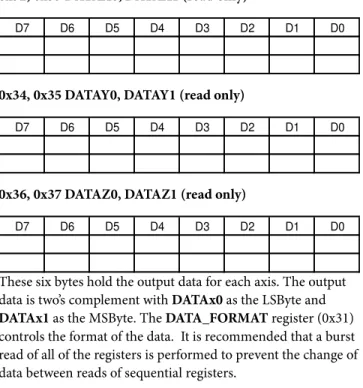
0x32, 0x33 DATAX0, DATAX1 (read only)
D7 D6 D5 D4 D3 D2 D1 D0
0x34, 0x35 DATAY0, DATAY1 (read only)
D7 D6 D5 D4 D3 D2 D1 D0
0x36, 0x37 DATAZ0, DATAZ1 (read only)
D7 D6 D5 D4 D3 D2 D1 D0
These six bytes hold the output data for each axis. The output data is two’s complement with DATAx0 as the LSByte and DATAx1 as the MSByte. The DATA_FORMAT register (0x31) controls the format of the data. It is recommended that a burst read of all of the registers is performed to prevent the change of data between reads of sequential registers.
0x38 FIFO_CTL (read/write)
D7 D6 D5 D4 D3 D2 D1 D0
TRIGGER
FIFO_MODE SAMPLES
FIFO_MODE: Corresponds to the FIFO Mode as shown in Table 15 below.
TRIGGER: A value of ‘0’ sets the trigger event of Trigger Mode
to INT1 and a value of ‘1’ sets the trigger event to INT2. SAMPLES: Function depends on the FIFO Mode as shown in
Table 16 below. Entering a value of zero in SAMPLES will immediately set the WATERMARK status bit in
INT_SOURCE, regardless of FIFO mode. Undesirable operation may occur if a value of zero is used for SAMPLES when Trigger Mode is used.
Table 15. FIFO Modes D7 D6 MODE Function
0 0 Bypass The FIFO is bypassed
0 1 FIFO FIFO collects up to 32 values then stops collecting data
1 0 Stream FIFO holds the last 32 data values. Once full, the FIFO’s oldest data is lost as it is replaced with newer data 1 1 Trigger When triggered by the TRIGGER the
FIFO holds the last 32 data values and stops when full.
Table 16. SAMPLES Functions
FIFO Mode Samples Function
Bypass None
FIFO Specifies how many FIFO entries are need to trigger a Watermark interrupt
Stream Specifies how many FIFO entries are need to trigger a Watermark interrupt
Trigger Specifies how many FIFO samples before the trigger event are retained in the FIFO buffer
0x39 FIFO_STATUS (read)
D7 D6 D5 D4 D3 D2 D1 D0
FIFO_TRIG X ENTRIES
FIFO_TRIG: A ‘1’ corresponds to a trigger event occurring while a ‘0’ means that a FIFO trigger event has not yet occurred. ENTRIES: Reports how many data values are stored in the
FIFO. To collect the data from the FIFO, access is through the standard DATAX, DATAY, and DATAZ registers. FIFO reads must be done in burst, or multi-byte, mode as each FIFO level is cleared after any read, single- or multi-byte, of the FIFO. The FIFO stores a maximum of 32 entries, which equates to a maximum of 33 entries available at any given time, due to the fact that an additional entry is available at the output filter of device.
APPLICATION
POWER SUPPLY DECOUPLING
In many applications, a 0.1 μF capacitor at VS and VDD I/O placed
close to the ADXL345 supply pins adequately decouples the accelerometer from noise on the power supply. However, in applications where noise is present at the 50 kHz internal clock frequency, or any harmonic thereof, additional care in power supply bypassing is required because this noise may cause errors in acceleration measurement. If additional decoupling is necessary, a 10 Ω resistor or ferrite in series with VS and an
additional larger bypass capacitor (2.2 µF or greater) at VS may
be helpful.
Care should be taken that the connection from the ADXL345 ground to the power supply ground be low impedance because noise transmitted through ground has an effect similar to noise transmitted through VS.
MECHANICAL CONSIDERATIONS FOR MOUNTING
The ADXL345 should be mounted on the PCB in a location close to a hard mounting point of the PCB to the case. Mounting the ADXL345 at an unsupported PCB location (that is, at the end of a “lever,” or in the middle of a “trampoline”), as shown in Figure 10, may result in large apparent measurement errors because the accelerometer will see the resonant vibration of the PCB. Locating the accelerometer near a hard mounting point ensures that any PCB resonances at the accelerometer are above the accelerometer’s mechanical sensor resonantfrequency and, therefore, effectively invisible to the accelerometer. MOUNTING POINTS PCB ACCELEROMETER 0 6 2 3 8 -0 1 4
Figure 10. Where Not to Mount an Accelerometer
TAP DETECTION
The tap interrupt function is capable of detecting either single or double taps. The following parameters are shown graphically in Figure 11 for a valid single and valid double tap event:
• Tap detection threshold is defined by the THRESH_TAP register.
until the opening of the time window, whose value is contained in the WINDOW register, for a possible second tap.
• The interval time after the expiration of LATENT is defined by the WINDOW register and is the period of time during which a second tap must begin. The second tap need not finish before the end of WINDOW.
FIRST TAP
TIME LIMIT FOR TAPS (DUR)
LATENCY TIME (LATENT)
TIME WINDOW FOR SECOND TAP (INTVL)
SECOND TAP
SINGLE TAP INTERRUPT DOUBLE TAP INTERRUPT
THRESHOLD (THRESHC) XH I B W IN T 0 6 2 3 8 -0 1 1
Figure 11. Tap Interrupt Function with Valid Single and Double Taps If only the single tap function is in use, the single tap interrupt will trigger at the point that the acceleration goes below the threshold as long as DUR is not exceeded. If both single and double tap functions are in use the single tap interrupt will trigger once the double tap event has been either validated or invalidated.
Several events can occur to invalidate the second tap of a double tap event. First, if the SUPPRESS bit in the TAP_AXES register is set, any acceleration spikes above the threshold during the LATENT time window will invalidate the double tap as seen in Figure 12.
XH
I
B
W
INVALIDATES DOUBLE TAP IF SUPPRESS BIT SET
XH
I
B
W
INVALIDATES DOUBLE TAP IF SUPPRESS BIT SET
Rev. PrA | Page 19 of 24
A double tap event can also be invalidated if an acceleration above the threshold is detected at the start of WINDOW, resulting in an invalid double tap at the start of WINDOW, shown in Figure 13. Additionally, a double tap event can be invalidated by having an acceleration exceed DUR, resulting in an invalid double tap at the end of DUR for the second tap event, also seen in Figure 13.
XH I B W XH I B W TIME LIMIT FOR TAPS (DUR) LATENCY TIME (LATENT)
TIME WINDOW FOR SECOND TAP (WINDOW)
TIME LIMIT FOR TAPS (DUR) TIME LIMIT FOR TAPS (DUR)
INVALIDATES DOUBLE TAP AT START OF WINDOW INVALIDATES DOUBLE TAP AT END OF DUR XH I B W XH I B W TIME LIMIT FOR TAPS (DUR) LATENCY TIME (LATENT)
TIME WINDOW FOR SECOND TAP (WINDOW)
TIME LIMIT FOR TAPS (DUR) TIME LIMIT FOR TAPS (DUR)
INVALIDATES DOUBLE TAP AT START OF WINDOW
INVALIDATES DOUBLE TAP AT
END OF DUR
Figure 13. Tap Interrupt Function with Invalid Double Taps Single taps, double taps, or both may be detected by setting their respective bits in the INT_ENABLE register. Control over participation of each of the three axes in tap/double tap detection is exerted by setting the appropriate bits in the TAP_AXES register. For the double tap function to operate, both LATENT and WINDOW must be non-zero.
Every mechanical system will have somewhat different tap/double tap response based on the system’s mechanical characteristics, so some experimentation with values for the LATENT, WINDOW, and THRESH_TAP registers will be required. In general a good starting point is LATENT>0x10, WINDOW>0x10, and THRESH_TAP>3g. Setting very low values in the LATENT, WINDOW, and/or THRESH_TAP registers may result in unpredictable response due to the accelerometer picking up “echoes” of the tap inputs. After a tap interrupt is received, the first axis to exceed the THRESH_TAP level is reported in the ACT_TAP_STATUS register. This register is never cleared, but overwritten with new data.
THRESHOLD
The lower Output Data Rates are achieved by decimation of a common sampling frequency inside the device. The activity, free-fall and tap/double tap detection functions are performed using the un-filtered data. Since the output data is filtered, the high frequency and high-g data that is used to determine activity, free-fall and tap/double tap events may not be present if the output of the accelerometer is examined. This may result in trigger events appearing to occur when acceleration does not appear to trigger an event, such as exceeding a threshold or remaining below a threshold for a certain period of time.
LINK MODE
The LINK function can be used to reduce the number of activity interrupts the processor must service by only looking for activity after inactivity. For proper operation of the link feature, the processor must still respond to the activity and inactivity interrupts by reading the INT_SOURCE register to clear them. If the activity interrupt is not cleared, the part will not go into Auto Sleep Mode. The ASLEEP bit in the
ACT_TAP_STATUS register indicates if the part is in Auto Sleep Mode.
RECOMMENDED PWB LAND PATTERN
3.3400 0.5500 0.2500 3.0500 0.2500 1.1450 0.3400 1.0500 0 6 2 3 8 -0 1 5Figure 14. Recommended Printed Wiring Board Land Pattern (Dimensions Shown in Millimeters)
Rev. PrA | Page 21 of 24
RECOMMENDED SOLDERING PROFILE
tP tL t25°C TO PEAK tS PREHEAT CRITICAL ZONE TL TO TP T E M P E R A T U R E TIME RAMP-DOWN RAMP-UP TSMIN TSMAX TP TL 0 6 2 3 8 -0 1 6
Figure 15. Recommended Soldering Profile
Table 17. Recommended Soldering Profile1
Condition
Profile Feature Sn63/Pb37 Pb-Free
Average Ramp Rate (TL to TP) 3°C/sec max 3°C/sec max
Preheat
Minimum Temperature (TSMIN) 100°C 150°C
Maximum Temperature (TSMAX) 150°C 200°C
Time (TSMIN to TSMAX)(tS) 60 sec to 120 sec 60 sec to 180 sec
TSMAX to TL
Ramp-Up Rate 3°C/sec max 3°C/sec max Time Maintained Above Liquidous (TL)
Liquidous Temperature (TL) 183°C 217°C
Time (tL) 60 sec to 150 sec 60 sec to 150 sec
Peak Temperature (TP) 240 + 0/−5°C 260 + 0/−5°C
Time Within 5°C of Actual Peak Temperature (tP) 10 sec to 30 sec 20 sec to 40 sec
Ramp-Down Rate 6°C/sec max 6°C/sec max Time 25°C to Peak Temperature 6 minutes max 8 minutes max
OUTLINE DIMENSIONS
Figure 35. 14-Lead Land Grid Array Package [LGA] 3 mm × 5 mm Body, Thick Quad Dimensions shown in millimeters
Lead finish: matte tin
ORDERING GUIDE
Model Measurement Range Specified Voltage (V) TemperatureRange Package Description
Package Option
ADXL345BCCZ1 ±2, 4, 8, 16g 2.5 −40°C to +85°C 14-Lead Land Grid Array
Package [LGA]
TBD ADXL345BCCZ–RL1 ±2, 4, 8, 16g 2.5 −40°C to +85°C 14-Lead Land Grid Array
Package [LGA]
TBD ADXL345BCCZ–RL71 ±2, 4, 8, 16g 2.5 −40°C to +85°C 14-Lead Land Grid Array
Package [LGA]
TBD EVAL-ADXL345Z1 Evaluation Board
1 Z = Pb-free part.
Rev. PrA | Page 23 of 24