VYSOKÉ UČENÍ TECHNICKÉ V BRNĚ
BRNO UNIVERSITY OF TECHNOLOGYFAKULTA ELEKTROTECHNIKY A KOMUNIKAČNÍCH TECHNOLOGIÍ
ÚSTAV MIKROELEKTRONIKY
FACULTY OF ELECTRICAL ENGINEERING AND COMMUNICATION
DEPARTMENT OF MICROELECTRONICS
NÁVRH ANALOGOVÝCH OBVODŮ S NÍZKÝM
NAPÁJECÍM NAPĚTÍM A NÍZKÝM PŘÍKONEM.
LOW VOLTAGE LOW POWER ANALOGUE CIRCUITS DESIGN.DIZERTAČNÍ PRÁCE
DOCTORAL THESISAUTOR PRÁCE Ing. ZIAD ALSIBAI
AUTHOR
VEDOUCÍ PRÁCE Doc. Ing. et Ing. FABIAN KHATEB, Ph.D. et Ph.D.
ABSTRACT
The dissertation thesis is aiming at examining the most common methods
adopted by analog circuits' designers in order to achieve low voltage (LV) low
power (LP) configurations. The capability of LV LP operation could be
achieved either by developed technologies or by design techniques. The thesis is
concentrating upon design techniques, especially the non–conventional ones
which are bulk–driven (BD), floating–gate (FG), quasi–floating–gate (QFG),
bulk–driven floating–gate (BD–FG) and bulk–driven quasi–floating–gate (BD–
QFG) techniques. The thesis also looks at ways of implementing structures of
well–known and modern active elements operating in voltage
–, current
–, and
mixed
–mode such as operational transconductance amplifier (OTA), second
generation current conveyor (CCII), fully–differential second generation current
conveyor (FB–CCII), fully–balanced differential difference amplifier (FB–
DDA), voltage differencing transconductance amplifier (VDTA), current–
controlled current differencing buffered amplifier (CC–CDBA) and current
feedback operational amplifier (CFOA). In order to confirm the functionality
and behavior of these configurations and elements, they have been utilized in
application examples such as diode–less rectifier and inductance simulations, as
well as low–pass, band–pass and universal filters. All active elements and
application examples have been verified by PSpice simulator using the 0.18 µm
TSMC CMOS parameters. Sufficient numbers of simulated plots are included in
this thesis to illustrate the precise and strong behavior of structures.
KEYWORDS
Low voltage, low power, analog circuit design, bulk–driven transistor, floating–
gate transistor, quasi–floating–gate transistor, active filter, active element.
ABSTRAKT
Disertační práce je zaměřena na výzkum nejběžnějších metod, které se využívají
při návrhu analogových obvodů s využití nízkonapěťových (LV) a
nízkopříkonových (LP) struktur. Tyto LV LP obvody mohou být vytvořeny díky
vyspělým technologiím nebo také využitím pokročilých technik návrhu.
Disertační práce se zabývá právě pokročilými technikami návrhu, především pak
nekonvenčními. Mezi tyto techniky patří využití prvků s řízeným substrátem
(bulk-driven - BD), s plovoucím hradlem (floating-gate - FG), s kvazi
plovoucím hradlem (quasi-floating-gate - QFG), s řízeným substrátem s
plovoucím hradlem (bulk-driven floating-gate - BD-FG) a s řízeným substrátem
s kvazi plovoucím hradlem (quasi-floating-gate - BD-QFG). Práce je také
orientována na možné způsoby implementace známých a moderních aktivních
prvků pracujících v napěťovém, proudovém nebo mix-módu. Mezi tyto prvky
lze začlenit zesilovače typu OTA (operational transconductance amplifier), CCII
(second generation current conveyor), FB-CCII (fully-differential second
generation current conveyor), FB-DDA (fully-balanced differential difference
amplifier), VDTA (voltage differencing transconductance amplifier), CC-CDBA
(current-controlled current differencing buffered amplifier) a CFOA (current
feedback operational amplifier). Za účelem potvrzení funkčnosti a chování výše
zmíněných struktur a prvků byly vytvořeny příklady aplikací, které simulují
usměrňovací a induktanční vlastnosti diody, dále pak filtry dolní propusti,
pásmové propusti a také univerzální filtry. Všechny aktivní prvky a příklady
aplikací byly ověřeny pomocí PSpice simulací s využitím parametrů technologie
0,18 µm TSMC CMOS. Pro ilustraci přesného a účinného chování struktur je v
disertační práci zahrnuto velké množství simulačních výsledků.
KLÍČOVÁ SLOVA
Nízké napětí, nízký příkon, návrh analogových obvodů, tranzistor řízený
substrátem, tranzistor s plovoucím hradlem, tranzistor s kvazi plovoucím
hradlem, aktivní filtry, aktivní prvky.
DECLARATION
I declare that I have elaborated my doctoral thesis on the theme of “Low Voltage Low Power Analogue Circuits Design” independently, under the supervision of the doctoral thesis
supervisor and with the use of technical literature and other sources of information which are all quoted in the thesis and detailed in the list of literature at the end of the thesis.
Brno . . . ……….. (Author’s signature)
ACKNOWLEDGMENTS
I would like to express my gratitude to my supervisor, Doc. Ing. et Ing. Fabian
Khateb, Ph.D. et Ph.D. who has provided me with guidelines for my work and
has supported me with valuable advices through my studies.
I would also like to express my sincerest gratitude to my parents, Fatima and
Adib, as well as my brothers, Mazen and Ghiyath, for their unwavering support
throughout this personal ordeal. Even though I have stumbled many times over
the years, they have always been there to prop me back up. I could not have
reached this point in my life without them.
Faculty of Electrical Engineering and Communication
Brno University of Technology
Technicka 12, CZ-61600 Brno, Czech Republic http://www.six.feec.vutbr.cz
Výzkum popsaný v této disertační práci byl realizován v laboratořích
podpořených z projektu SIX; registrační číslo CZ.1.05/2.1.00/03.0072, operační
program Výzkum a vývoj pro inovace.
LIST OF ABBREVIATIONS
AC Alternating Current APF All Pass Filter AVR Average Value Ratio A/D Analog to Digital BD Bulk Driven
BD FG Bulk Driven Floating Gate BD QFG Bulk Driven Quasi Floating Gate BJT Bipolar Junction Transistor BOX Buried OXide
BPF Band Pass Filter BSF Band Stop Filter CC Current Conveyor
CCI First Generation Current Conveyor
CCII Second Generation Current Conveyor CCIII Third Generation Current Conveyor CCCII Current Controlled Current Conveyor
CCCDBA Current Controlled Current Differencing Buffered Amplifier CCTA Current Conveyor Transconductance Amplifier
CDU Current Differencing Unit
CDBA Current Differencing Buffered Amplifier
CDTA Current Differencing Transconductance Amplifier CDVB Current Differencing Voltage Buffer
CE Characteristic Equation CF Current Follower
CFA Current Feedback Amplifier
CFOA Current Feedback Operational Amplifier CGCCII Current Gain Current Conveyor
CMRR Common Mode Rejection Ratio
CMOS Complementary Metal Oxide Semiconductor CS Common Source
DCVC Differential Current Voltage Conveyor DDA Differential Difference Amplifier
DDCC Differential Difference Current Conveyor DOTA Dual Output OTA
DOCCII Dual Output CCII
DVCCII Differential Voltage CCII
DVCCS Differential Voltage Controlled Current Source
EEPROM Electrically Erasable Programmable Read Only Memory EPROM Erasable Programmable Read Only Memory
FDCCII Fully Differential Second Generation Current Conveyor
FG Floating Gate FN Fowler–Nordheim GB Gain Bandwidth GD Gate Driven HPF High Pass Filter IC Integrated Circuit
KHN Kerwin_Huelsman_Newcomb LP Low Power
LPF Low Pass Filter LV Low Voltage
MIFG Multi Input Floating Gate
MOOTA Multiple Output Operational Transconductance Amplifier MOSFET Metal Oxide Semiconductor Field Effect Transistor MOST MOSFET Transistor
OC Oscillation Condition OF Oscillation Frequency OPA Operational Amplifier
OTA Operational Transconductance Amplifier
OTA_C Operational Transconductance Amplifier_Capacitor QFG Quasi Floating Gate
QO Quadrature Oscillator RMS Root Mean Square RMSE Root Mean Square Error SIMO Single Input Multiple Output SNR Signal to Noise Ratio
SOC System on Chip SOI Silicon On Insulator
PSpice Simulation Program with Integrated Circuit Emphasis THD Total Harmonic Distortion
TSMC Taiwan Semiconductor Manufacturing Company UCC Universal Current Conveyor
UV Ultra Violet VB Voltage Buffer VC Voltage Conveyor
VCCS Voltage Controlled Current Source
VDTA Voltage Differencing Transconductance Amplifier VF Voltage Follower
VLSI Very large scale integration VM Voltage Mode
LIST OF SYMBOLS
C capacitorCBC total bulk channel capacitance
Cbd bulk to drain parasitic capacitance
Cbs bulk to source parasitic capacitance
Cbsub bulk to substrate parasitic capacitance
CGC total gate channel capacitance
Cgd gate to drain parasitic capacitance
Cgs gate to source parasitic capacitance
Cj zero bias junction capacitance
Cload load capacitor
COX gate oxide capacitance per unit area
D denominator of transfer function
ΔVT mismatch between the threshold voltages of PMOST and NMOST
ƐOX dielectric permittivity
Ɛsi permittivity of silicon
F surface potential
f frequency
fc cut off frequency
fT transition frequency
fT,b transition frequency of BD MOST
fT,FG transition frequency of FG MOST
fT,QFG transition frequency of QFG MOST
slope factor
φ phase
γ bulk–threshold parameter
gds,eff effective output conductance of FG MOST/QFG MOST
G conductance
GBW gain bandwidth product
gm transconductance
gm,b bulk transconductance
gm, eff effective transconductance
gm,QFG quasi floating gate transconductance
Ibias bias current of the transconductance
IDSsat drain source current in saturation
ID0 process dependent parameter
ILeakage sub–threshold leakage current
K transconductance parameter
µ0 free electron mobility in the channel
L inductor
λ channel length modulation coefficient
ω0 pole frequency
Pavg average power
Pdynamic dynamic power
Pstatic static power
Q quality factor
q charge of an electron
QFG residual charge trapped at the FG during the fabrication process
R resistor
Rlarge largevalue resistor
Rleak leakage resistance
ro output resistance
s=jω complex parameter – Laplace operator
tOX oxide thickness
tsi thickness of the depletion layer between the channel and the bulk
V terminal voltage of an active element
VBS bulk to source voltage
VDD, VSS supply voltages of CMOS structure
VDS drain to source voltage
VFG voltage at FG in FG MOST
VGS gate to source voltage
v2
noise input referred noise power spectral density
VQFG voltage at FG in QFG MOST
VT threshold voltage
CONTENTS
1. INTRODUCTION ... 20
References ... 23
2. STATE OF THE ART ... 24
2.1. SURVEYOFLOW–VOLTAGEDESIGNTECHNIQUES ... 26
2.1.1 Conventional low–voltage techniques ... 26
2.1.1.1 Circuits with rail–to–rail operating range ... 27
2.1.1.2 MOS transistors operating in weak inversion region ... 30
2.1.1.3 Level shifter technique ... 31
2.1.1.4 MOS transistors in self–cascode structure ... 33
2.1.2 Non–conventional low–voltage techniques ... 35
2.1.2.1 Bulk–driven MOST ... 35
2.1.2.2 Floating–gate approach ... 40
2.1.2.3 Quasi–floating–gate approach ... 45
2.1.2.4 Bulk–driven floating–gate and bulk–driven quasi–floating–gate approach... 49
2.1.2.5 Comparison between non–conventional low–voltage techniques ... 52
2.2. SUB–CONCLUSION ... 56
References ... 57
3. THESIS OBJECTIVES AND RESULTS ... 61
3.1. OPERETIONAL TRANSCONDUCTANCE AMPLIFIER (OTA) ... 61
3.1.1. Bulk–driven quasi–floating–gate operational transconductance amplifier (BD– QFG OTA) ... 62
3.1.1.1 BD–QFG OTA–based diode–less precision rectifier ... 63
3.1.1.2 Simulation results ... 65
3.1.2. Floating–gate operational transconductance amplifier (FG OTA) ... 74
3.1.2.1 FG OTA based tunable voltage differencing transconductance amplifier (FG VDTA) ... 75
3.1.2.2 Simulation results ... 77
3.2. CURRENTCONVEYOR(CC) ... 80
3.2.1 Bulk–driven second–generation current conveyor (BD CCII) ... 83
3.2.1.1 BD–CCII–based inductance simulations ... 84
3.2.1.2 Simulation results ... 84
3.3. FULLY DIFFERENTIAL CCII (FD–CCII) ... 86
3.3.1 Bulk–driven fully differential current conveyor (BD FD–CCII) ... 87
3.3.1.1 BD–FDCCII–based universal filter ... 89
3.3.1.2 Simulation results ... 90
3.3.2 Bulk–driven quasi–floating–gate fully differential current conveyor (BD–QFG FD–CCII) ... 94
3.3.2.1 BD–QFG–FDCCII–based universal filter ... 97
3.4. FULLY BALANCED DIFFERENTIAL DIFFERENCE AMPLIFIER (FB– DDA) 102
3.4.1 Bulk–driven quasi–floating–gate fully–balanced differential difference amplifier
(BD–QFG FB–DDA) ... 104
3.4.1.1 BD–QFG FB–DDA–based band–pass filter ... 104
3.4.1.2 Simulation results ... 105
3.5. CURRENTDIFFERENCINGBUFFEREDAMPLIFIER(CDBA) ... 110
3.5.1. Bulk–driven z–copy current–controlled current differencing buffered amplifier (BD ZC CC CDBA) ... 111
3.5.1.1 BD–ZC–CC–CDBA–based universal filter ... 113
3.5.1.2 Simulation results ... 114
3.6. CURRENT FEEDBACK OPERATIONAL AMPLIFIER (CFOA) ... 116
3.6.1. Floating–gate differential difference current feedback operational amplifier (FG–DD–CFOA) ... 117
3.6.1.1 FG–DDCFOA–based universal filter ... 119
3.6.1.2 Simulation results ... 120
3.7. SUB–CONCLUSION ... 123
References ... 124
4. CONCLUSION ... 130
LIST OF TABLES
Tab. 2.1. PD–SOI vs. FD–SOI. ... 25
Tab. 2.2. Relations of transconductance, threshold voltage, output conductance and transient frequency for GD, BD, FG, QFG, BD–FG, and BD–QFG MOSTs operating in saturation region. .... 53
Tab. 3.1. Transistors aspect ratios for Fig. 3.2. ... 65
Tab. 3.2. BD–QFG OTA performance benchmark indicators. ... 66
Tab. 3.3. Summary of the performance for OTA. ... 78
Tab. 3.4. Measurement results of the transconductance. ... 78
Tab. 3.5. Measurement conditions of the circuit. ... 78
Tab. 3.6. Transistors dimensions. ... 78
Tab. 3.7. FG OTA performance benchmark indicators. ... 78
Tab. 3.8. Frequency ranges and bandwidths for different values of Ibias2. ... 80
Tab. 3.9. Transistors aspect ratios for Fig.3.24. ... 85
Tab. 3.10. Summarized performances of proposed BD–QFG–FDCCII ... 85
Tab. 3.11. Transistors aspect ratios for Fig. 3.31. ... 91
Tab. 3.12. Summarized performances of proposed BD–FDCCII. ... 91
Tab. 3.13. Component values and transistors aspect ratios for Fig. 3.38. ... 99
Tab. 3.14. Summarized performances of proposed BD–QFG–FDCCII. ... 99
Tab. 3.15. Performance comparison of BD–QFG FDCCII with other FDCCIIs... 100
Tab. 3.16. The comparison of BD–QFG FDCCII–based filter with previously FDCCII–based filters. ... 100
Tab. 3.17. Component values and transistor aspect ratios for the BD–QFG FB–DDA in Fig. 3.48. . 106
Tab. 3.18. Simulation results of the BD–QFG FB–DDA compared to DDA and FB–DDA. ... 108
Tab. 3.19. The transistors aspect ratios of the circuit shown in Fig. 3.57. ... 115
Tab. 3.20. The most important characteristics of the circuit in Fig. 3.57. ... 115
Tab. 3.21. Transistor aspect ratios for Fig. 3.71. ... 120
LIST OF FIGURES
Fig. 1.1. A plot of the recent trends seen in VT and VDD for standard TSMC bulk CMOS processes. .. 21
Fig. 1.2. Amplitudes and spectral ranges of some important biosignals. ... 22
Fig. 2.1. Simplified cross section of an NMOST (P–well CMOS technology). ... 24
Fig. 2.2. FD–SOI starting wafer. ... 25
Fig. 2.3. Double–gate FinFET. ... 26
Fig. 2.4. Rail–to–rail input commom–mode stage. ... 27
Fig. 2.5. Transconductance variations versus input common–mode voltage. ... 27
Fig. 2.6. Adding a floating voltage source at the inputs of the differential pair to implement common– mode response shaping. ... 29
Fig. 2.7. Transconductance variations vs. input common–mode stage in Fig. 2.6. ... 29
Fig. 2.8. Current mirror: (a) simple, (b) based on level shifter technique. ... 32
Fig. 2.9. (a) Self–cascode structure, (b) equivalent composite transistor. ... 34
Fig. 2.10 Bulk–driven NMOST: (a) symbol and (b) cross–section. ... 36
Fig. 2.11. Bulk–driven MOS transistor (a), and its equivalent JFET (b). ... 36
Fig. 2.12. (a) CS amplifier based on BD MOST. (b) CS amplifier based on GD MOST. (c) small signal equivalent circuit of the BD based CS amplifier. (d) small signal equivalent circuit of the GD based CS amplifier. ... 37
Fig. 2.13. Circuits for calculating transition frequency of BD MOST: (a) AC schematic, (b) small signal equivalent circuit. ... 38
Fig. 2.14. Two–input floating–gate NMOST: (a) symbol, (b) equivalent circuit, (c) layout and (d) cross–section. ... 41
Fig. 2.15. Floating–gate MOST: (a) common source amplifier and (b) small signal model equivalent circuit. ... 42
Fig. 2.16. Circuit for calculating transition frequency of FG– MOST: (a) AC schematic, (b) small signal equivalent circuit. ... 43
Fig. 2.17. One–input quasi–floating–gate NMOST: (a) symbol, (b) its equivalent circuit and (c) layout. ... 46
Fig. 2.18. Quasi–floating–gate MOST: (a) common source amplifier with single input terminal, (b) small signal model equivalent of (a). ... 47
Fig. 2.19. Circuit to calculate transition frequency of QFG MOST: (a) ac schematic, (b) small signal equivalent circuit. ... 48
Fig. 2.20. Symbols of the BD–FG MOST (a) and BD–QFG MOST (b). ... 50
Fig. 2.21. Realization in MOS technology for BD–FG MOST (a) and BD–QFG MOST (b). ... 50
Fig. 2.22. Small–signal models for BD–FG and BD–QFG MOSTs. ... 51
Fig. 2.23. Common–source amplifier based on: conventional GD (a), BD (b), FG (c), QFG (d), BD– FG (e), and BD–QFG (f) MOSTs... 55
Fig. 2.24. Drain currents versus gate–source of GD MOST, bulk–source of BD MOST, gate–source of FG–MOST, gate–source of QFG–MOST, gate–bulk–source of BD–FG–MOST and BD–QFG–MOST voltages of N–MOSTs from Fig. 2.23. ... 56
Fig. 3.1. Ideal operational transconductance amplifier, (a) symbol and (b) equivalent circuit. ... 62
Fig. 3.6 Frequency response of OTA as a voltage follower. ... 67
Fig. 3.7. DC transfer characteristic and voltage error of the BD-QFG OTA of Fig. 3.2. ... 68
Fig. 3.8. DC transfer characteristic of BD-QFG Half-wave rectifier. ... 69
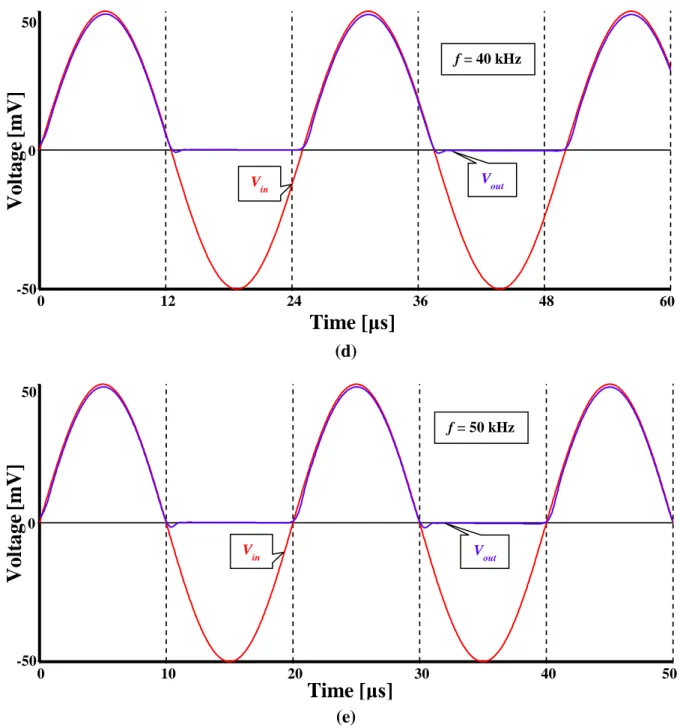
Fig. 3.9. Transient analyses of output waveforms with 15 kHz and various amplitudes of the input signal. ... 70
Fig. 3.10. Transient analyses of input and output waveforms with Vm= 50 mV and (a) 10 (b) 20 (c) 30 (d) 40 and (e) 50 kHz. ... 72
Fig. 3.11. Outputs waveforms at different temperatures. ... 73
Fig. 3.12. AVR (Average Value Ratio) (a) and RMS error (b) versus frequency for three amplitudes of the input voltage (50, 100, 150) mV. ... 74
Fig. 3.13. The circuit of two–stage OTA using FG–MOSTs. ... 74
Fig. 3.14. VDTA element as a connection of two MO–OTAs. ... 76
Fig. 3.15. Single–input multiple–output biquad filter based on FG VDTA. ... 77
Fig. 3.16. Frequency response of FG–OTA. ... 79
Fig. 3.17. Input and output signals vs. time. ... 79
Fig. 3.18. Zout vs. frequency. ... 79
Fig. 3.19. Simulated frequency responses of low-pass and band–pass signals shown in Fig. 3.6. ... 80
Fig. 3.20. Low-pass filter peaking vs. Q (Gm1 is variable). ... 80
Fig. 3.21. Band–pass filter when Ibias2 is varied (Gm2 is variable). ... 80
Fig. 3.22. CCI block representation. ... 81
Fig. 3.23. Matrix description of (a) CCI, (c) CCII and (e) CCII. Nullator–norator model for: (b) CCI, (d) CCII and (f) CCIII. ... 82
Fig. 3.24. Proposed BD–CCII. ... 83
Fig. 3.25. BD–CCII–based grounded inductance simulations. ... 84
Fig. 3.26. DC curve Vx versus Vy and errors (VCM=0.25V). ... 86
Fig. 3.27. DC curve Iz versus Ix and error. ... 86
Fig. 3.28. Simulated impedance value versus frequency. ... 86
Fig. 3.29. Simulated transient responses response with input signal 1 kHz and amplitude 200 mVp–p. 86 Fig. 3.30. FD–CCII (a) matrix characteristic (b) block scheme. ... 87
Fig. 3.31. Proposed BD–FDCCII. ... 88
Fig. 3.32. BD–FDCCII–based universal filter. ... 90
Fig. 3.33. Simulated Vxp and Vxn versus Vy1 for different of Vy2. ... 92
Fig. 3.34. Simulated Izp and Izn versus Vy1 when Rxp=Rxn=10 k. ... 92
Fig. 3.35. The equivalence input and output noise against frequency. ... 92
Fig. 3.36. Simulated HPF, LPF, BPF and BSF responses. ... 92
Fig. 3.37. The input and output waveforms of the BPF response for a 10 kHz sinusoidal input voltage of 100 mV (peak). ... 93
Fig. 3.38. Proposed BD–QFG–FDCCII. ... 96
Fig. 3.39. Universal filter using BD–QFG–FDCCII. ... 98
Fig. 3.40. Simulated Vxp and Vxn versus Vy1 for different of Vy2. ... 101
Fig. 3.41. Simulated Izp and Izn versus Vy1 when Rxp = Rxn = 10 k. ... 101
Fig. 3.42. Simulated HPF, BSF, BPF, and LPF responses. ... 101
Fig. 3.43. Simulated gain and phase of APF responses. ... 101
Fig. 3.44. Simulated BPF filter with adjustable Q. ... 102
Fig. 3.45. The input and output waveforms of the BPF response for a 31.6 kHz sinusoidal input voltage of 100 mV (peak). ... 102
Fig. 3.46. DDA (a) schematic symbol (b) matrix characteristic. ... 103
Fig. 3.48. CMOS implementation of the FB–DDA with CMFB circuit using BD–QFG transistors. . 104
Fig. 3.49. Sallen–Key band–pass filter. ... 105
Fig. 3.50. The AC gain and phase responses. ... 106
Fig. 3.51. The transient response with input signal 4 kHz and amplitude 80 mV where FB–DDA is connected as a fully differential voltage follower. ... 107
Fig. 3.52. The DC response of the BD–QFG FB–DDA connected as a fully differential voltage follower. ... 108
Fig. 3.53. Simulated magnitude response BP filter. ... 109
Fig. 3.54. The input and output waveforms of filter for a 200 Hz sinusoidal input voltage of 120 mV (peak-to-peak). ... 109
Fig. 3.55. CDBA (a) matrix characteristic (b) block scheme. ... 110
Fig. 3.56. ZC–CC–CDBA: (a) schematic symbol, (b) equivalent circuit. ... 111
Fig. 3.57. The proposed MOS structure of the ZC–CC–CDBA. ... 112
Fig. 3.58. Parasitic resistances Rp and Rn versus the bias current Ibias. ... 112
Fig. 3.59. Current mode biquad filter based on ZC–CC–CDBA. ... 113
Fig. 3.60. DC curves Iz, Izc versus Ip and In. ... 115
Fig. 3.61. DC curves Iz, Izc versus Ip for various values of In. ... 115
Fig. 3.62. Frequency responses of the current gains Iz,zc/Ip, Iz,zc/In. ... 115
Fig. 3.63. Frequency response of the parasitic impedances of z and zc terminals. ... 115
Fig. 3.64. DC curves Vw versus Vz and the voltage error Vz–Vw. ... 116
Fig. 3.65. AC curve of the voltage gain VW/VZ. ... 116
Fig. 3.66. Frequency dependence of the parasitic impedance of w terminal. ... 116
Fig. 3.67. Frequency response of the proposed filter. ... 116
Fig. 3.68. The response of the band pass filter for different IB1 values. ... 116
Fig. 3.69. The response of the band pass filter for different values of IB1, IB2 and IB3. ... 116
Fig. 3.70. Circuit symbol of CFOA. ... 117
Fig. 3.71. Proposed FG–DDCFOA. ... 118
Fig. 3.72. Symbol of: conventional DDCFOA (a) DDCFOA and (b) proposed FG–DDCFOA. ... 118
Fig. 3.73. FG–DDCFOA–based universal filter. ... 120
Fig. 3.74. Simulated Vx versus Vy1 when Vy2 is parameter. ... 121
Fig. 3.75. Simulated Iz versus Vy1 when Vy2 is parameter. ... 121
Fig. 3.76. Simulated Vo versus Vy1 when Vy2 is parameter. ... 122
Fig. 3.77. Simulated magnitude response of BP, LP and HP filters. ... 123
Fig. 3.78. The input and output waveforms of the BPF response for a 10 kHz sinusoidal input voltage of 130 mV (peak–to–peak). ... 123
1.
INTRODUCTION
In the last decade, with the continuous scaling in the feature size of the transistors, nominal supply voltage of CMOS integrated circuits has been dramatically decreased due to the strongly emerging consumer market for portable devices that needed to be light weighted and hence operate for a long period of time with a small battery. When a MOS transistor size is scaled down, the thickness of the gate oxide is reduced. As a MOS transistor has a thinner gate oxide, in order to prevent the transistor from a breakdown due to higher electrical field across the gate oxide, and to ensure its reliability, the supply voltage needs to be reduced [1–5]. Therefore, low–voltage (LV) low–power (LP) analog circuits have received significant attention and have become increasingly important in the electronic industry. Recent advances in LV LP circuit design made it possible to conceive electronic systems that could be worn by people, monitor physiological parameters, and even provide some kind of treatment [6]. The primary application targets of these circuits are low power Systems–on–Chips (SOCs). That covers markets such as: Mobile Internet Services (Smartphones, Tablets, Netbooks), Cellular Telecom, Home and Mobile Multimedia, etc. SOCs are circuits composed of analog and digital components co–existing on a single chip. The idea of SOC came up originally from universal fact that the outside world is mostly analog in nature and that the bandwidth of a signal can become a magnitude higher if the signal is processed in analog circuits. Thus, it became inevitable to introduce analog signal processing. However, when switched to low supply voltage, digital circuits do not suffer lower performance, but the circuit performances of analog circuits, such as gain, dynamic range, speed, bandwidth, linearity, etc. are strongly affected by reduced supply voltage [7]. In addition, chip area reduces the cost of advanced multi–function SOC design. Moreover, LP SOCs need to combine demanding dynamic performance with low power consumption. Therefore, there is urgent need to develop new design techniques for analog circuits at 1–V supply which consume levels of power in the nanowatt range. However, the advances in VLSI technology, circuit design, and product market are actually interrelated. In the past decade, CMOS technology has played a major role in the rapid advancement and the increased integration of VLSI systems. CMOS devices feature high input impedance, extremely low offset switches, high packing density, low switching power consumption, and thus can be easily scaled. The minimum feature size of a MOS transistor has been scaled down to around 90 nm. Consequently, more circuit components in a single chip can then be integrated, so the circuit area and thus its cost will be reduced. In addition, smaller geometry usually lowers the parasitic capacitance, which leads to higher operating speed.
However, system portability usually requires battery supply and therefore weight/energy storage considerations. For the time being, battery technologies do not proportionally evolve with the speed of the applications demand. Therefore the challenge is to
reduce the power consumption of the circuits. In any case, average power, Pavg, consumed by
these circuit, consists of the sum of two components, static and dynamic power:
f V C I V P P
Pavg static dynamic DD leakage DD2 , (1.1) where VDD is power supply voltage, Ileakage is sub–threshold leakage current of MOS
transistor, C represents the total capacitance of a system, and f denotes the frequency at which a circuit operates. Among the most important factors of CMOS VLSI processes is the threshold voltage of the MOS devices VT. However, since a MOST’s sub–threshold leakage
current, Ileakage, is exponentially dependent upon the threshold voltage, VThas not been able to
decline as quickly as VDD does in each new process generation because of concerns over
increasing Pavg through Pstatic. Therefore, for instance, for five standard IBM bulk CMOS
processes, the ratio of VT/VDDhas increased noticeably – from VT/VDD= 0.5 V/2.5 V = 0.2 to
VT/VDD = 0.29 V/1 V = 0.29 – between IBM’s 0.25 μm and 65 nm nodes [8–12]. As one
would expect, this trend shall continue on until the end of bulk CMOS scaling, at which point,
VDD and VT/VDD are predicted to reach 0.70 V and 0.355, respectively [13]. Another example
in order to show how disproportionately VT and VDD have fallen in recent years is shown in
Fig. 1.1 where the two parameters are plotted for six standard TSMC bulk CMOS processes [14].
0
1
2
3
250
180
130
90
65
40
S
u
p
p
ly
a
n
d
t
h
re
sh
o
ld
V
o
lt
a
g
e
[
V
]
Technology [nm]
VT VDDFig. 1.1. A plot of the recent trends seen in VT and VDD for standard TSMC bulk CMOS processes.
On the other hand, the new trend of the design of modern implantable or portable biomedical devices is toward miniaturization and portability for long–term monitoring.
bioimpedance, biomechanical, biochemical and biomagnetic signals [15]. All these signals have very low amplitude in the range of microvolts to millivolts. For example, EEG signals (Electroencephalography signals), which are bioelectric signals, are varying between 5 and 100 microvolts [16]. Other bioelectric signals such as ECG (Electrocardiography), EMG (Electromyography), ERG (Electroretinography) and ENG (Electronystagmography) have about the same value of amplitude. Bioelectric signals (AKA Biosignals) are recorded as potentials, voltages, and electrical field strengths generated by nerves and muscles. Due to their low–level amplitude, integrated circuits are essential to be designed for the amplification of the weak signals before any further signal processing can be performed to make them compatible with devices such as displays, recorders, or A/D converters for computerized equipment. Amplifiers, adequately, have to measure these signals, satisfying very specific requirements. They have to provide amplification responsive to physiological signal, rejecting superimposed noise and interference signals, and guaranteeing protection from damages through voltage and current surges for both patient and electronic equipment. Amplifiers featuring these specifications are what we call biopotential amplifiers. In fact, amplifying such low voltages is very challenging. Fig. 1.2 shows an overview of the most commonly measured biopotentials, and specifies the normal ranges for amplitude and bandwidth [17]. To maintain a reasonable signal to noise ratio while minimizing energy consumption to maximize the useful life of the implant, the designer needs to use special circuit techniques and make difficult design compromises. I will address this issue in more detail later.
Fig. 1.2. Amplitudes and spectral ranges of some important biosignals.
The thesis is organized as follows: in section 2, a state–of–the–art of conventional and non–conventional techniques and structures, as well as developed technologies, which could
be implemented to obtain LV LP circuits is done. In section 3, circuits, in addition to application examples for them to prove their functionality, are designed using LV LP techniques. Finally, the main conclusions of this thesis are presented in section 4.
References
[1] J. E. Chung, M. C. Jeng, J. E. Moon, P. K. Ko, and C. Hu, “Performance and reliability design issue for deep–submicrometer MOSFET’s,” IEEE Transactions on Electron Devices, vol. 38, no. 3, pp. 545–554, Mar. 1991.
[2] T. H. Ning, P. W. Cook, R. H. Dennard, C. M. Osburn, S. E. Schuster, and H. N. Yu, “1 um MOSFET VLSI technology: Part IV – hot–electron design constraints,” IEEE J. Solid–StateCircuits, vol. 14, no. 2, pp. 268– 275, Apr. 1979.
[3] C. Hu, S. C. Tam, F. C. Hsu, P. K. Ko, T. Y. Chan, and K. W. Terrill, “Hot–electron–induced MOSFET degradation–model, monitor, and improvement,” IEEE Transactions on Electron Devices, vol. 35, no. 7, pp. 375–385, Feb. 1985.
[4] R. W. Brodersen, “The network computer and its future,” IEEE Int. Solid–State Circuits Conf. Dig. Tech.
Papers, pp. 32–36, Feb. 1997.
[5] H. Yasuda, “Multimedia impact on devices in the 21st century,” IEEE Int. Solid–State Circuits Conf. Dig.
Tech. Papers, pp. 28–31, Feb. 1997.
[6] E. Rodriguez–Villegas, P. Corbishley, C. Lujan–Martinez, and T. Sanchez–Rodriguez, “An ultra–low– power precision rectifier for biomedical sensors interfacing,” Sensors and Actuators A: Physical, vol. 153, no. 2, pp. 222–229, 2009.
[7] T.–Y. Lo and C.–C. Hung, 1V CMOS Gm–C Filters: Design and Applications. Springer, 2009. [8] “IBM CMOS6SF Model Reference Guide,” Nov. 2006.
[9] “IBM CMOS7SF Model Reference Guide,” Oct. 2008. [10] “IBM CMOS8SF Model Reference Guide,” Sep. 2008. [11] “IBM CMOS9SF Model Reference Guide,” Apr. 2006. [12] “IBM CMOS10SF Model Reference Guide,” May 2007.
[13]International Technology Roadmap for Semiconductors, ITRS 2007 Edition. Available Online:
http://www.itrs.net/Links/2007ITRS/Home2007
[14]TSMC Technology Overview (MPW). Available Online: http://www.europractice–
ic.com/technologies_TSMC.php?tech_id=025um
[15]Physiology of Biomedical Signals. Available Online:
http://www.engr.sjsu.edu/mkeralapura/editable/Download/Physiologyofsignals
[16]ELECTROCARDIOGRAPHY ECG. Available Online: http://ulb.upol.cz/lectures/vaa11/eldg
[17]J. H. Nagel, Biopotential Amplifiers. The Biomedical Engineering Handbook, Second Edition. Boca Raton: CRC Press LLC, 2000.
2.
STATE OF THE ART
Low–voltage low–power capability could be achieved either by developed technologies or by design techniques [1]. Since developed technologies are out of the scope of this thesis they will be mentioned briefly. The main technologies used for LV LP IC design are:
CMOS technology [2]: is a MOS technology integrates both N–channel and P–channel
transistors on the same chip. If the substrate of the circuit is P–doped, the N–channel
transistors sit directly on the substrate, whereas the P–channel devices need a well
(tube). The technology is termed N–well technology. For an N–type substrate the
arrangement is complementary: the P–channel transistors are made in the substrate
and the N–channel transistors sit inside the P–well (Fig. 2.1 [3]). CMOS technology is
used in the fabrication of conventional microchips, since it is less expensive than BiCMOS and SOI technologies and offers high performance, high density and low– power dissipation.
Fig. 2.1. Simplified cross section of an NMOST (P–well CMOS technology).
BiCMOS technology [4, 5]: this technology integrates BJT and CMOS transistor in a single integrated circuit, thus combines the advantages of both. A number of advantages can be achieved using this advanced semiconductor technology such as: improving speed over purely bipolar technology, lowering power dissipation over purely CMOS technology, improving current drive over CMOS and packing density over bipolar, and obtaining high input impedance, low output impedance, high gain, low noise, high analog performance, flexible I/Os for high performance, latch–up immunity, smaller IC size and of more reliable IC. However, BiCMOS technology requires extra fabrication steps, the matter which makes the technology not cost– effective.
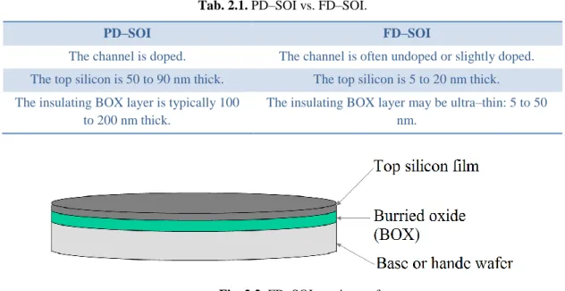
SOI (Silicon On Insulator) technology [6–10]: in this technology a layer of silicon dioxide is implanted below the surface by oxidation of Si or by oxygen implantation into Si. This implanted silicon dioxide is called buried oxide (BOX) and helps reducing parasitic capacitances, and as a result improves the performance of the device. SOI can be divided into two categories, fully depleted FD and partially
D S B
P–well
Sub N–epi N+ N+ P+ N+depleted PD, the main differences are summarized in Tab. 2.1. Fig. 2.2 shows a starting wafer of FD–SOI.
Tab. 2.1. PD–SOI vs. FD–SOI.
PD–SOI FD–SOI
The channel is doped. The channel is often undoped or slightly doped. The top silicon is 50 to 90 nm thick. The top silicon is 5 to 20 nm thick. The insulating BOX layer is typically 100
to 200 nm thick.
The insulating BOX layer may be ultra–thin: 5 to 50 nm.
Fig. 2.2. FD–SOI starting wafer.
SOI technology has many advantages such as capacitance reduction, reduced short channel effects, lower device threshold, lower supply voltage, soft error rate effects, ideal device isolation, smaller layout area, high switching speed and lower–power consumption. However, fabrication of this technology is more expensive featuring also higher self–heating because of poor thermal conductivity of the insulator.
Multi–gate transistors [11–14]: amongst the different types of SOI devices proposed, one clearly stands out: the multi–gate field–effect transistor (multi–gate FET). A multi–gate transistor is a MOST which incorporates more than one gate into a single device. This device has a general “wire–like” shape with a gate electrode that controls the flow of current between source and drain. Multi–gate FETs are commonly referred to as “multi(ple)–gate transistors”, “wrapped–gate transistors”, “double–gate transistors”, “FinFETs”, “tri(ple)–gate transistors”, “Gate–all–Around transistors”, etc. The distinguishing characteristic of the FinFET is that the conducting channel is wrapped by a thin silicon "fin", which forms the body of the device. The thickness of the fin (measured in the direction from source to drain) determines the effective channel length of the device. Fig. 2.3 shows a double–gate FinFET device. A multi– gate device employing independent gate electrodes is sometimes called a Multiple Independent Gate Field Effect Transistor (MIGFET). The International Technology Roadmap for Semiconductors (ITRS) recognizes the importance of these devices and calls them “Advanced non–classical CMOS devices”.
S o u rc e Fin G a te D ra in
Fig. 2.3. Double–gate FinFET.
On the other hand, low–voltage design techniques are divided into two categories: conventional and non–conventional. All LV design techniques will be discussed in the next sub–section including principle of operation, small signal models of non–conventional techniques and main advantages and disadvantages of each technique.
2.1.
SURVEY OF LOW–VOLTAGE DESIGN TECHNIQUES
Among the most important factors of CMOS VLSI processes is the threshold voltage of the MOS devices VT. However, since a MOST’s sub–threshold leakage current, Ileakage, is
exponentially dependent upon the threshold voltage, VT has not been able to decline as
quickly as the power supply voltage VDD does in each new process generation because of
concerns over increasing Pavg through Pstatic. Another factor prevents the threshold voltage
from being scaled down by the same ratio is that devices with higher threshold voltage value have higher noise margin and smaller leakages. In order to overcome this restriction many techniques have been introduced in the literature based on CMOS technology. By utilizing these techniques, the threshold voltage is decreased or –in some cases– even removed.
2.1.1 Conventional low–voltage techniques
The most widely used conventional techniques for low–voltage low–power analog circuits design are:
1) Circuits with rail–to–rail operating range.
2) MOS transistors operating in weak inversion region. 3) Level shifter technique.
2.1.1.1Circuits with rail–to–rail operating range
Usually, gate–source voltage prevents the input stage from reaching the positive and/or negative supply voltages within the range of a threshold voltage; the value of this threshold voltage varies depending on semiconductor manufacturing process. This becomes a serious issue when the supply voltage is as low as 1 V or less in battery–powered systems or in low–power applications. A solution to this problem includes designing an input stage with a rail–to–rail common–mode input–voltage range allowing input common–mode signals to vary from negative to positive supply rails by the use of complementary differential pairs operated in parallel as shown in Fig. 2.4. [15, 16].
VSS VDD M1 M2 M3 M4 Vin1 Vin2 Ib2 Ib1 R2 R1 R3 R4
Fig. 2.4. Rail–to–rail input common–mode stage.
Three common–mode input voltage ranges can be distinguished as shown in Fig. 2.5: 1) In the range from the negative supply voltage VSS to VSS+ VT only the PMOS pair Ml,
M2 is operating.
2) In the range from the positive supply voltage VDD to VDD – VT only the NMOS pair M3,
M4 is operating.
3) In the intermediate range both pairs are operating.
When the common–mode voltage moves from one range into another, the transconductance of the input stage changes by a factor of two. Because of this, the total transconductance is not constant across the input common–mode range. This is an undesired phenomenon because it not only results in non–constant gain and variable unity–gain frequency but also degrades the common–mode rejection ratio (CMRR) and causes the slew rate to vary. This prevents frequency compensation from being optimal since the bandwidth is proportional to that transconductance. Moreover, transient distortion occurs when fast changes in the common–mode voltage abruptly saturate and restore the tail–current sources.
A number of techniques have been proposed to achieve constant gm[17–32]. A simple
technique could be adopted to reduce the variations in the small–signal response of rail–to– rail input stage consists in shifting the common–mode response of one input pair so the curves of gmp and gmn shown in Fig. 2.5 overlap [33, 34]. With this approach, provided that the two
differential pairs are perfectly matched, variations in the total amplifier transconductance can only arise in the common transition region of the two pairs, and are much lower with respect to the traditional composite rail–to–rail input stages [33]. Authors in [33], inspiring from [30] and [31], achieved adequate common–mode response shifting by connecting two floating and constant voltage sources VS between the input signals and the gate terminals of one of the
input pairs as shown in Fig. 2.6.
In Fig. 2.6, an appropriate positive value of VS shifts the takeover region of the PMOS
input pair, as seen by the signal inputs Vin1 and Vin2, to a Vi,cm voltage range closer to the
negative supply voltage. In [33, 34], authors also presented a technique in order to further decrease the total amplifier transconductance deviations, which mainly arise in the overlapping takeover regions, and named this technique as common–mode response shaping. According to their approach, the floating voltage sources have a variable value, which is a function of the input common–mode voltage [i.e., VS = f (Vi,cm)]. Resulting variations in the
VSS VDD M1 M2 M3 M4 Vin1 Vin2 Vs MBN MBP Vs
Fig. 2.6. Adding a floating voltage source at the inputs of the differential pair to implement common– mode response shaping.
Fig. 2.7. Transconductance variations vs. input common–mode stage in Fig. 2.6.
Advantages
1) Obtaining an acceptable SNR (signal–to–noise ratio) in low–voltage environments [17– 20, 24, 28, 30, 32, 35–42].
2) Circuits with rail–to–rail operating range can be used in low voltage analog design. 3) Rail–to–rail operation which allows input common–mode signals to vary from the
negative to positive supply rails.
Disadvantages
1) Circuit complexity to obtain a constant transconductance value over the input voltage range.
2.1.1.2MOS transistors operating in weak inversion region
Another way to reduce the current levels and hence the power consumption of a circuit is by using MOS transistors biased in the weak inversion (or sub–threshold) region driving very low current levels. It is well known that in a NMOS transistor under the condition of drain–source voltage is greater than saturation voltage, when gate–source voltage exceeds an extrapolated value called threshold voltage VT the MOST works in strong inversion (or
saturation) region, and when it does not the MOST operates in weak inversion region. Actually, there is a region between these two regions called moderate inversion region, but for simplicity we will ignore this region and suppose that the transition between the weak and the strong inversion regions occurs abruptly.
In weak–inversion region, the applied gate–source voltage is barely larger (or even slightly less) than the threshold voltage of the NMOS transistor so a channel between the drain and the source is not established, but the aforementioned voltage is high enough so it creates a depletion layer at the surface of the silicon. Thus, in this region, the channel charge is much less than the charge in the depletion region so the drain current arising from the drift of majority carriers is negligible. When VDS > Vther (around 3 Vther which is about 78 mV) and
VGS < VT, the current in this case is attributed to diffusion in the region and is given by:
ther T GS D DS V V V I L W I exp 0 . (2.1)
ID0 is process–dependent parameter which is dependent also on bulk–source and
threshold voltages. ID0 is given by:
L W V C
IDO 2 ox ther2 , (2.2)
where is the weak inversion slope factor and lies between 1.2 and 2, Vther is the thermal
voltage and equals 26 mV at room temperature and the other parameters have usual meanings. Note from the equation that the current is independent of VDS and exponentially
proportional to the overdrive voltage. Again this result is valid only for big values ofVDS.
The transconductance of an MOST operating in weak inversion is identical to that of a corresponding bipolar transistor except for the factor of 1/:
ther DS m V I g . (2.3) Since the current in sub–threshold region is so small, the transconductance is expected to be very small.
Transconductance to current ratio is, however, a better criterion since it shows how efficiently the current is used to generate transconductance. This ratio of an MOST in weak inversion is given by:
ther DS m V I g 1 , (2.4) which is independent of the current and the overdrive. Again, since the current is the lowest in weak inversion region, the transconductance to current ratio is the highest among any region of operation. Thus for high gain this region is preferred.
Last but not least, in weak inversion CgsCgd0 where Cgs and Cgd are gate–source
and gate–drain parasitic capacitances, respectively. Thus input capacitance Cin, which is
approximately Cgb, can be thought of as the series combination of the oxide and depletion
capacitors, as well as the transconductance is small as mentioned. Therefore the transition frequency fT becomes very small because of the relationship:
in m T C g f 2 . Advantages
1) The ability to work in very low voltage environment, and here we are talking about just dozens of millivolts even for cascode structures.
2) Very suitable to be used in very low–power low–frequency applications such in the biomedical applications where operating frequencies range between 1 Hz to 1 kHz.
Disadvantages
1) Increased chip area.
2) Slow speed because of the low value of fT as mentioned earlier.
2.1.1.3Level shifter technique
In conventional two–transistor current mirror shown in Fig. 2.8 (a), the input transistor M1 is used in diode connected configuration and an input voltage Vin is required to pump Iin
into the input port. Here, Vin depends solely on the biasing conditions of M1, which operates
in saturation mode. Thus, this topology requires Vin of at least one threshold voltage VT.
In level shifter technique, a MOST (or more) is inserted at the input port so that input voltage required is reduced to minimum. Fig. 2.8 (b) [43] shows a current mirror based on level shifter technique, from the circuit we note that Vin = VDS1 = VGS1 – VGS3. So if we made
VGS3 VGS1, Vin would approximately equal zero.
Assuming low bias current Ibias is presented; M3 operates in the sub–threshold region
for the entire input current Iin range. The operation of M1 and M2 depends on their aspect
ratios and on Iin. Hence, when Iin < 1A, M1 and M2 operate in the sub–threshold region and
when Iin exceeds l A they operate in the saturation region.
Practically, even with zero Iin, M1 and M2 work in weak inversion region, and this is
Vin Vbias VDS1 VGS1 VSS (a) Iin Iout M1 M2 Vin Vbias VDS1 VGS1 VSS (b) Iin Iout M1 M2 Ibias VDD VGS3 M3
Fig. 2.8. Current mirror: (a) simple, (b) based on level shifter technique.
The offset current will be given by: ther T bias DO DO offset V V I I I W L L W I exp 3 2 3 3 2 2 , (2.5)
where IDO2, IDO3, and Vther have been introduced before and ΔVT is the mismatch between
the threshold voltages of PMOST and NMOST.
Equation (2.5) indicates that Ioffset can be tailored according to the designers' need
through the appropriate selection of W and L.
Threshold voltage mismatch ΔVT depends on particular CMOS technology. Even if
the threshold voltages of PMOST and NMOST are matched and IDO2 = IDO3, Ioffset cannot be
reduced tozero. The lower limit of Ioffset equals Ibias
W L L W 3 3 2 2 . So to ensure low I offset, appropriate
values for W/L of M2 and M3 must be taken and Ibias must be as low as possible.
So far, we assumed that Ibiasis low, but if we considered the case when Ibiasis high the
situation would be completely different. In this case, Ibias drives M3 into the saturation region;
but M1 will be in linear mode due to low input current. However, M2 will operate in the saturation region because the external bias voltages will decide its drain voltage. In this situation the offset current is given by:
2 3
3 2 2 2 2 TP V TN V bias I Ioffset . (2.6) If threshold voltages of NMOST and PMOST were matched, the offset current would be: bias offset I W L L W K K I 3 3 2 2 3 2 , (2.7)where K2 and K3 are the transconductance parameters for M2 and M3, respectively. The ratio’s value of 3 2 K K
is usually around 3 which makes the offset current sufficiently high, so
Ibias must always be kept as low as possible to reduce Ioffset and to keep the ratio of
3 2
K K
away from the calculation of Ioffset.
Advantages
1) The input resistance is low, which is desirable for current mode circuits. 2) The bandwidth at low voltage is higher.
3) Rail–to–rail and low voltage operation.
Disadvantages
This technique utilizes more transistors which increases the power dissipation.
2.1.1.4MOS transistors in self–cascode structure
Along with the scaling of MOST size, the output impedance is reducing since it is proportional to channel length (or more accurately to effective channel length). Thus the gain is also degrading.
A solution to this problem could be in using the cascode structure, but although this technique increases the output impedance, it decreases the output signal swing, thus cascode structure cannot be used in low voltage systems [43].
Because it does not require high compliance voltages at output nodes, self–cascode (SC) configuration shown in Fig. 2.9 (a) [44] provides high output impedance with larger voltage headroom than the conventional cascode structure offers. This approach has potential applications in low voltage design.
A self–cascode structure can be treated as a single composite transistor (as shown in Fig. 2.9 (b)) operating in saturation region but without severe channel–length modulation effects. The composite structure has much larger effective channel length and the effective output conductance is much lower.
M1 M2 mW/L W/L X G D S i M S G D (a) (b)
Fig. 2.9. (a) Self–cascode structure, (b) equivalent composite transistor.
The lower transistor M1 operates in non–saturation (linear) region. Depending on the drain voltage, transistor M2can work in saturation or linear region.
For the composite transistor to work in saturation region; M2 should work in saturation region and M1 should workin linear region. Thus, we can write equations for these two transistors as:
VGS VX VT
VGS VT VX VX i 2 1 2 1 2 2 . (2.8) Solving i we obtain:
2 2 1 T GS eq V V i , (2.9) where 2 1 2 1 eq is the effective transconductance.
For optimal operation the W/L ratio of M2 should be larger than that of M1 by the factor of m so that m>1. If 2 m1then: 1 2 1 1 1 1 m eq eq m m m . (2.10) So if we kept the channel length the same for both transistors and made W2 wide
The equivalent output impedance of the composite transistor is: 2 ) 1 ( o M o m r r . (2.11) The effective transconductance of the composite transistor is approximately equal to the transconductance of M1: 1 2 M m M m eff m g m g g . (2.12)
As mentioned before, M1 usually works in linear region, so the voltage between its drain and source is so small that there is no considerable difference between VDSAT of
composite and simple transistors.
Advantages
1) The SC structure offers high output impedance similar to a regular cascode structure while output voltage requirements are similar to that of a single transistor.
2) Unlike cascode circuits, SC circuit does not require additional real–estate and power for its operation [45].
Disadvantages
Its drawbacks are limited input common mode range and small output swing.
2.1.2 Non–conventional low–voltage techniques
The most widely used non–conventional approaches for low–voltage low–power analog circuits design are:
1) Bulk–driven MOST. 2) Floating–gate approach. 3) Quasi–floating–gate approach.
4) Bulk–driven floating–gate and bulk–driven quasi–floating–gate approach.
2.1.2.1Bulk–driven MOST
Bulk–driven MOST (BD MOST) concept was first proposed by A. Guzinski et al in 1987 [46]. After that and as evidenced in the literature during the last years, BD technique has been adopted to implement a number of analog building blocks such as operational amplifiers [47–51], current mirrors [52–54], current conveyors, [55], [56], operational transconductance amplifiers [47], [49], [57–61], voltage followers [62], [63], voltage to current converters [64], buffers [65], voltage–controlled oscillators [66], and phase–locked loops [67]. An NMOST and its cross–section are shown in Fig. 2.10.
Sub
S
N-substrate
B
G D
P-well
N-EPI
n+ p+ n+ n+(a)
(b)
D
S
B
G
Fig. 2.10 Bulk–driven NMOST: (a) symbol and (b) cross–section.
In BD technique, a bias voltage is applied to the gate of the MOST so a channel is established between the source and the drain. This channel remains constant as long as the gate bias voltage is still the same, as the case for BD technique. On the other hand, the signal is applied to the bulk contact. By this way, the limitation of threshold voltage on the signal pathway is eliminated; consequently, the applicability of any analog cell to a very low supply voltage is possible to be extended.
Since the bulk contact serves the function of the gate of JFET and modulates the channel width according to the voltage applied to the bulk (see Fig. 2.11), BD MOST is considered as a depletion type device. For N–channel (P–channel), BD MOST can work in
negative (positive), zero or slightly positive (negative) biasing condition.
Vin M1 Vbias VDD VSS Ibias (a) Vin VDD M2 Ibias VSS (b)
Fig. 2.11. Bulk–driven MOS transistor (a), and its equivalent JFET (b).
An important aspect in analog design is small signal analysis. To study the small signal equivalent circuit of BD MOST in comparison with the small signal equivalent circuit of gate–driven MOST (GD MOST), BD and GD common–source (CS) amplifiers are shown in Fig. 2.12 (a,b), and the small signal equivalent circuits at high frequencies of the SC amplifiers are shown in Fig. 2.12 (c,d).
(a) VDD VSS Vbias MBD RD Vin Vout
BD MOST based CS amplifier
(b) VDD VSS MGD RD Vin Vout
GD MOST based CS amplifier
D B S S Sub (c) Vin=Vbs Cbd Cbsub Cbs gmbVbs ro RD Vout
Small signal equivalent circuit of (a)
(d) D G S S Cgd RD ro gmVgs Cgs Vout Vin=Vgs
Small signal equivalent circuit of (b)
Fig. 2.12. (a) CS amplifier based on BD MOST. (b) CS amplifier based on GD MOST. (c) Small signal equivalent circuit of the BD based CS amplifier. (d) Small signal equivalent circuit of the GD based CS
amplifier.
The capacitances Cbd, Cbs, Cbsub are bulk–drain, bulk–source and bulk–substrate
parasitic capacitances, respectively. These parasitic capacitances are a result of well and substrate structure of the transistor.
The relationship between threshold voltage and bulk–source voltage in BD MOST is:
) 2 2 ( 0 F BS F T T V V V . (2.13)
With + for an NMOST and – for PMOST where VT is the threshold voltage, VBS is the
bulk–source voltage, VT0 is the threshold voltage at zero bulk–source voltage, γ and F are the
bulk–threshold parameter and the surface potential, respectively.
The transconductance of GD MOST which operates in strong inversion is given by:
) ( gs T m v V L W k g , (2.14) where k is the current gain factor of the used process. However, the transconductance of BD MOST is given by:
m m GC BC m BS F b m g g C C g V g 0.2 0.4 2 2 , , (2.15) where CBC and CGC are the total bulk–channel and the total gate–channel parasiticcapacitances, respectively.
To determine the frequency performance of a transistor, transition frequency fT must
be calculated. To calculate fT, consider the AC circuit in Fig. 2.13 (a) and the small signal
equivalent in Fig. 2.13 (b). Vbs Cbd Cbsub Cbs gmbVbs
(b)
Vbs in i iout(a)
out i in i MBDFig. 2.13. Circuits for calculating transition frequency of BD MOST: (a) AC schematic, (b) small signal equivalent circuit.
The small signal input current iin:
bs bd bsub bs in s C C C v i ( ) . (2.16) If the current through Cbd is neglected then iout:
bs mb out
g
v
i
. (2.17) From (2.16) and (2.17) we can calculate the current gain:) ( bs bsub bd mb in out C C C s g i i . (2.18)
We substitute s with jw then we get:
) ( bs bsub bd mb in out C C C j g i i . (2.19) The magnitude of the small signal current gain is unity when:
bd bsub bs mb C C C g T . (2.20)
bd bsub bs mb T b T C C C g f 2 1 2 1 , . (2.21) Assuming that (Cbs + Cbsub) is much greater than Cbd, then:
T bsub bs mb b T f C C g f (0.3 0.5) ) ( 2 , , (2.22) whereas fT is transition frequency of GD MOST which can be calculated by following the
same steps: gs T C g f m 2 . (2.23)
From (2.22) it is obvious that the transition frequency of BD MOST is smaller than the transition frequency of GD MOST, since the transition frequency is proportional to the transconductance, as well as the effect of the parasitic capacitances.
The input referred noise power spectral density of GD MOST is expressed by:
2 2 2 , m ni GD noise g i v , (2.24)
where i2ni is the total drain current generated by noise sources and its unit is A2. The input
referred noise power spectral density of BD MOST can be expressed by:
2 , 2 2 , noiseGD mb m BD noise v g g v . (2.25)
BD MOST suffers from higher referred noise as it is clear from (2.25), since gm,b is
inherently smaller than gm.
BD MOST and GD MOST have identical output resistance ro as we can notice from
Fig. 2.12 and its value is given by:
DSsat o o I g r 1 1 . (2.26) Advantages
1) As mentioned, N–channel bulk–driven MOST works in negative, zero or slightly
positive bias voltage also. This can lead to larger input common mode voltage range and voltage swing that could not otherwise be achieved at low power supply voltages. 2) Depletion characteris


![Tab. 3.2. BD–QFG OTA performance benchmark indicators. Parameters Proposed OTA Koziel [105] Majumdar [106] Li [107] Zhang [108] CMOS Technology [µm] 0.18 0.5 0.35 0.35 0.18 Power supply [V] ± 0.3 ± 2.5 3.3 3.3 1.8 Power consumption](https://thumb-us.123doks.com/thumbv2/123dok_us/268433.2527558/66.892.124.781.130.789/performance-benchmark-indicators-parameters-proposed-majumdar-technology-consumption.webp)