Conducted Electro Magnetic Interference Spectral
Peak Mitigation in Luo Converter Implementation
Using FPGA Based Chaotic PWM Technique
Sudhakar Natarajan 1, Sanjeevikumar Padmanaban 2,*, Thanikanti Sudhakar Babu 1
1 School of Electrical Engineering, VIT University, Vellore, Tamilnadu, India; [email protected]; [email protected]
2 Department of Energy Technology, Aalborg University, Esberg 6700, Denmark; [email protected]
* Correspondence: [email protected]; [email protected]; Tel.: +97-960-011-7935
Abstract: Chaotic switching is a newly evolve randomization method which can suppress
conducted electromagnetic interference generated within the DC-DC converter. It can suppress the spectral peaks present in the frequency band effectively by spread spectrum technique and can spread it over the wide range of frequency band implying EMI suppression. In this paper, a chaotic PWM technique based on RCFMFD scheme is generated through Field programmable gate array (FPGA) for suppressing the conducted electromagnetic interference (EMI) generated within the Luo converter. A hardware prototype of Luo converter was developed in order to analyze EMI reduction through FFT analysis by comparing both traditional periodic PWM switching and chaotic PWM switching. The results obtained from the hardware setup shows significant reduction of EMI with Chaotic switching as compared to traditional PWM switching for both boost and buck operation of Luo converter.
Keywords: EMI; Luo-converter; chaotic PWM technique; FPGA; RCFMFD.
1. Introduction
Electromagnetic interference (EMI) is one of the major issues which are faced by the industries and the users who deal with the electrical and electronic equipment on the daily basis. EMI is an undesirable noise which affects the performance of the electrical and electronics devices due to their electromagnetic radiation and conduction in the atmosphere [1]. Power conversion is one of the important fields in the industries and among various type of conversion used, DC-DC power conversion has wide employment in various applications such as regulated power supplies for computers, laptops, mobile phones, DC motor drives, electronic vehicles, telecommunications equipment and many more. EMI basically resulted from the high rate of change of voltage and current in the converters, has become a major design criterion in almost all DC–DC converters. Due to their fast switching action, DC-DC converters are main source as well as victim of EMI. So EMI is a very serious problem and has to be deal at designing level of DC-DC converter itself. Various international organizations like FCC, IEC and IEEE have made electromagnetic compatibility (EMC) standards and rules to be followed in order to reduce the effect of EMI and to keep the environment clean. Their main aim is to meet EMI regulations while not interfering with the performance of other applications nearby.
There are many methods which have been employed for suppressing EMI such as EMI filters EM shielding and soft switching technique [2]. All these conventional methods work as remedy, since they can suppress the EMI only when it is generated. Among various methods proposed in last few decades for EMI, randomization method proved to be promising method for suppressing EMI effectively at switching itself. Random PWM technique involves spread spectrum technique in which by varying any of the parameters such as pulse position or switching frequency can cause
suppression of spectral peaks (EMI noise) that get accumulated at multiple of switching frequency and spread it over a wide range of frequency band. Chaotic PWM technique is a type of random methods which are pseudo random in nature and can suppress the EMI noise effectively at switching itself. Chaotic modulation can be implemented in either in analogue or digital way. Among all the methods, chaotic PWM generation through field programmable gate array (FPGA) [3, 4] is the simplest method for implementation. It is a simple and less expensive technique which gives more accurate results.
Luo converter is a newly developed DC to DC converter which works on the principle of voltage lift technique [5]. This converter has simple structure and produce high positive output voltage with reduced ripples. It also possesses many advantage over conventional converters including reduced effect of parasitic elements, improved power density and efficiency. In voltage lift technique, output voltage is lifted up in arithmetic progression. Output voltage is lifted higher by charging and discharging of capacitor by source voltage in the circuit, where it arranged itself to rise up to a level of output voltage and is called as self-lift [6]. Series of Luo converters [7] are there which can also perform re-lift, super-lift and multiple-lift operation for higher voltage application by repeating the operation of voltage lift technique [8,9] in the circuit.
In this paper, FPGA based chaotic PWM technique is used for suppressing the conducted EMI generated in the DC-DC Luo converter. The paper is organized in following way. In section II, topology of Luo converter and its mode of operation are discussed in detail. Section III discusses about the chaotic modulation technique and chaotic PWM generation through FPGA. Section IV discusses about the simulation results and its hardware implementation by above discussed method in Luo converter.
2. Luo Converter
A. Circuit description
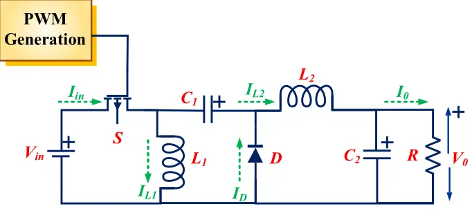
Luo converter can step up and step down the DC supply voltage depending on the duty ratio. It consists of a single switch S which can be driven by pulses having switching frequency f. The circuit consists of two parts- one is the pump circuit S-L1-D-C1 where voltage lifting action take place and other part is L2-C2 for filter action of output voltage. The circuit diagram of Luo converter is given below in the Figure 1.
B. Modes of operation
There are two modes of operation in Luo converter. During mode I switch is in on condition and in mode II, switch is in off condition.
Mode I:When switch S in on, diode D will be in off condition. Supply voltage Vin charges the
inductor L1 and inductor current IL1 start increasing. At the same instance, inductor L2 also starts absorbing energy from source voltage Vin and capacitor C1 and hence inductor current IL2 also start increasing. Thus average input current Iin become the sum of the two increasing inductor currents IL1 and IL2.
V
inR
L
2C
2D
S
L
1C
1V
0I
inI
L1I
L2I
0I
DPWM
Generation
V
inR
L
2C
2S
L
1C
1V
0I
inI
L1I
L2I
0Figure 2. Mode I- switch on condition
R
L
2D
L
1C
1V
0IL1
IL2
I
DFigure 3. Mode II- switch off condition
V
L1I
L1maxI
L1V
L2T
ONT
OFFt
t
t
t
t
dT (1-d)T
V
in-V
C1I
L1min(V
in+V
C1-V
0)
-V
0I
L2maxI
L2minI
L2V
C1Mode II: When switch S gets off, diode D turns on and performs the freewheeling action. Since
circuit get disconnected from source side, source current Iin becomes zero. Because of this, inductor current IL1 start reducing and flow through the freewheeling diode to charge the capacitor C1. At the same instance, inductor current IL2 start reducing through the circuit C2-R for making itself continuous in the circuit. The equivalent circuit diagram of Luo converter for switch on and switch off conditions [10] are shown in the Figure 2 and Figure 3 respectively.
The charge on capacitor C1 decreases and the current flowing through it is IL2 .Charge during on time can be equated as:
2
L
dTI
Q
(1)The charge on Capacitor C1start increasing and the current flowing through it is IL1.Charge during OFF time can be equated as:
1
)
1
(
d
TI
LQ
(2)Where d is the duty ratio and T
T
1f
is the total time period.For periodic operation,
Q
Q
Thus, L2
(
1
)
I
L1d
d
I
(3)Capacitor C2act as low pass filter at load side, so the output current Io is nearly equal to Inductor currentIL2.
2
L O
I
I
(4)Also, the value of source current is sum of two inductor currents during switch off time and zero during switch off. So the average source current can be calculated as
1 2 1
)
1
1
(
)
(
L L Lin
I
d
d
d
I
I
d
I
1
L in
I
I
(5)Hence, the output current obtain from (3), (4) and (5) is
in
O
I
d
d
I
1
(6)The average power supplied by the source side must be equal to the average power absorbed by the load:
O S
P
P
;V
inI
in
V
OI
O;in O O in
V
V
I
I
Hence, the output voltage is
in O
V
d
d
V
1
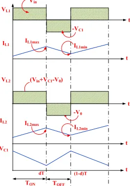
(7)We can see from the Figure 4, during switch on time, inductor L1 is charged through supply voltage,
in L
V
V
1
and during switch off condition, it is reversed biased by capacitor voltage,1
1 C
L
V
V
1
)
1
(
Cin
d
TV
dTV
in C
V
d
d
V
1
1Hence, capacitor voltage at C1 is
in O C
V
d
d
V
V
1
FF0 D Q
FF1 D Q
FF2 D Q
FF3 D Q
FF4 D Q
FF5 D Q
FF6 D Q
FF7 D Q
RESET Clock Pulse
LSB MSB
Figure 5. 8-bit linear feedback shift register
LUO Converter Driver
Circuit
FPGA Kit
RCFMFD
LSFR
Chaotic Pulse
Figure 6. Block diagram of CPWM generation
Start
Intialize PWM_PERIOD, PWM_ON and Count
Value=+1/3rd of Fsw
Positive edge clock
Counter=Counter+1
Counter<=PWM_Period Counter< PWM_ON
PWM_Signal, Fsw=1
A
PWM_Signal, Fsw=0
B A
NO
YES
NO
YES
Counter>PWM_period
Counter=1
PWM_ON=PWM_ Period
A B
A
PWM_Period=Count_ Value+LFSR_Output
NO
YES
Figure
7.
Flowchart depicting the generation of CPWM through RCFMFD based random2. Chaotic Pulse Width Modulation (CPWM)
Chaotic PWM technique is the newly proposed random method which has the feature of both spread spectrum and pseudo randomness[12]. Here PWM frequency varies chaotically and hence energy is distributed evenly to entire frequency spectrum. It involves pseudo-random modulationwhich appears to be random but is deterministic in nature. It generates random outputs which are produce ina sequence and can be repeated in a cycle.
A. Randomized carrier freuqency modulation with fixed duty ratio (RCFMFD)
Chaotic PWM pulses can be generated by applying different schemes in which parameters such as position, width or carrier frequency are varied. Among different schemes, randomized carrier frequency with fixed duty cycle (RCFMFD) is most famous scheme in which carrier frequency is varied by keeping the duty cycle constant. By randomizing the carrier frequency, central switching also gets randomized and by keeping the duty cycle constant, output voltage will not vary and gives a constant DC output. This scheme proved [13] to give low frequency harmonics spectrum on PSD and therefore chosen to be best option for switching scheme in DC-DC converters. While applying RCFMFD scheme, only consideration should be taken care is on the range of randomization of switching frequency. If carrier frequency is randomized more than a certain limit, it loses its property of EMI noise reduction and start overlapping with the successive frequency in the spectrum. This can be avoided by putting randomization range of switching frequency within the limit of ± one-third of central switching frequency. Chaotic PWM pulses can be generated by applying RCFMFD random scheme [13,14,15] along with pseudo number generator. Generation of random numbers can be done with the help of linear feedback shift register. It is discussed in detail in next section.
B. Linear feedback shift register
Random switching pulses can be generated with the help of linear feedback shift register (LFSR) which works on the principle of pseudo-random number generation. LFSR is a group of shift registers which use linear functions as a feedback mechanism to modify itself on each rising edge of the clock [14,15] which is shown in Figure 5. Here logic gates like XOR and XNOR gates are used as linear function to feedback the output bit to input bit. The input given at initial stage is called as ‘seed’. The bit positions, where next state is affected by linear functions are called as ‘taps’. The right most bit is the output bit. LFSR can produce maximum 2n-1 random numbers (except all 0), where n is the number of registers used. Since sequence generated is deterministic and finite, it can repeat the same stream of values from the initial stage until LFSR is clocked. It output is in the form of 1’s and 0’s.
C. Process of generating CPWM
Chaotic PWM pulses can be generated from LFSR by applying RCFMFD scheme on it. This whole process can be incorporated with FPGA. Block diagram depicting chaotic pulse generation is given in Figure 6.
Steps followed during the RCFMFD based chaotic PWM pulses generation [15] through FPGA for triggering the switch of Luo converter are given below:
1. At every positive edge of clock pulse, seed values (except all 0) given to LFSR.
2. With the help of XOR gates at particular tap, output bit is feedback to input and at the same time generates 2n-1 random values.
3. Random values generated in LFSR is fed to variable frequency generator which works on the basis of RCFMFD scheme.
4. In variable frequency generator, parameters such as PWM_PERIOD and PWM_ON are initialize and count value is set to maximum limit which is equal to ±1/3rd of central switching frequency.
6. On every positive edge of clock, increment the counter with 1 till it reaches to ON time. When counter reaches to PWM_ON value, then PWM pulse i.e. logic Fsw is becomes 1.
7. When counter exceeds the PWM_ON value, the logic Fsw becomes 0 and counter again start incrementing till it reaches PWM_PERIOD.
8. If counter exceeds the PWM_PERIOD value, then count value is reinitialize to 1.
9. Next PWM_PERIOD value is obtain by adding a constant count value which corresponds to maximum switching frequency with the output of LFSR.
10. Go to step 6, repeat all the steps for next cycle.
The steps followed for RCFMFD based random pulse generation is also be explained with the help of flowchart which is mention in Figure 7.
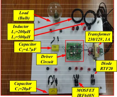
3. Prototype Hardware Implementation and Results
LOAD (BULB)
DRIVER CIRCUIT
TRANSFORMER 230/12 V, 1A
DIODE RTF20
MOSFET IRF 640N CAPACITOR
C1= 20uF
CAPACITOR C2= 4.7uF INDUCTOR
L1 =200uH L2=500uH Load (Bulb) Inductor L1=200μH
L2=500μH
Capacitor C2=4.7μF
Capacitor
C1=20μF MOSFET
IRF640N Diode RTF20 Transformer 230/12V, 1A Driver Circuit
Figure 8. A hardware prototype of Luo converter
Xilinx ISE Design suite 14.7
software
MSO
Xilinx Spartan 3E XC3S500E FPGA board
Load Driver circuit
Luo converter Regulated DC power supply Regulated DC Power Supply Luo Converter Driver Circuit Load
Xilink ISE Design
suite 14.7 Software MSO
Xilink Spartan 3E XC3S500E FPGA
Board
Figure 9. Complete hardware setup
Table 1. Prototype Experimental Specification
Specifications Values
Input voltage, Vin 12 V Output voltage, Vo 24 V
Power rating, P 40 Watts Switching frequency, f 200 KHz Load (resistive) 14.8 ohms
Inductor, L2 500µH
Capacitor, C1 20µF
Capacitor, C2 4.7µF
In order to verify the RCFMFD scheme based chaotic PWM technique for conducted EMI suppression [16,17,18], a hardware prototype of Luo converter is designed and developed with the given specification in Table 1. Prototype of Luo converter is shown in Figure8 and complete hardware setup is shown in Figure 9.
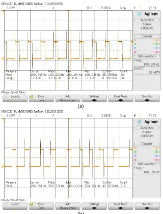
(a)
(b)
(a)
(b)
Figure 11. Pulses for buck operation with 0.33 duty cycle and switching frequency (a) Periodic pulse (b) Chaotic pulse in the range of ± 1/3rd of 200 KHz
(b)
Figure 12. FFT of output voltage for duty cycle of 0.67(a) periodic pulses (b) chaotic pulses
(b)
Figure 13. FFT of output voltage for duty cycle of 0.33 for (a) Periodic pulses (b) Chaotic pulses
For generation of periodic and chaotic PWM pulses [19], programming is done in Xilinx ISE design suite 14.7 software and is interfaced with Xilinx Spartan 3E XC3S500E FPGA board. The oscillator frequency of this FPGA board is 50MHz and can be down scale for desired frequency. The pulses generated from with Xilinx Spartan 3E XC3S500E FPGA [20] is fed to the driver circuit which boost up the voltage of FPGA (3.3 V) to trigger the switch of Luo converter.
Both periodic and chaotic pulses generated from FPGA board for boost and buck operating modes of Luo converter are shown in Figure 10(a), Figure 10(b), Figure 11(a) and Figure 11(b) respectively. For boost operating mode, design specification is Vin=12V, Vo=24V with duty cycle of 0.67 and switching frequency of 200 kHz whereas for buck operating mode Vin= 24V, Vo=12V with duty cycle of 0.33 and switching frequency of 200 kHz.
After getting pulses through the FPGA board, FFT analysis is done on the output voltage obtained from the Luo converter. Output voltage along with FFT obtained is shown in Figure 12 (a), 12(b), 13 (a) and 13(b) for duty cycle of 0.67 and 0.33 respectively. In Fig 12 (a) with periodic pulses, average of peak noise obtain is at – 52 dBV which is equal to 2.5mV, whereas In Fig 12 (b) with chaotic pulses, it occurs at -60 dBV which is equal to 1mV. It can be seen that there is reduction of approximately 8dBV which is equal to 1.5mV of conducted noise in chaotic mode as compared to periodic mode. In Figure13 (a) of Luo converter with periodic pulses, average peak noise obtains is at 66.47 dBV which is equal to 0.47mV whereas in Figure13 (b)with chaotic pulses, it occurs at -73.15 dBV which is equal to 0.22 mV. It can be seen that there is reduction of approximately 7dBV which is equal to 0.25mV of conducted noise in chaotic mode as compared to periodic mode.
4. Conclusion
References
[1] H. Li, Z. Li, B. Zhang, W.S.K. Tang and W.A. Halang. Suppressing electromagnetic interference in DC converters. IEEE circuits and system magazine. 2009; 9:10-28.
[2] N. Sudhakar, N. Rajasekar, N. Rohit, E. Rakesh and J. Jacob. EMI mitigation in closed loop boost converter using soft switching combined with chaotic mapping. IEEE conference on Advances in electrical
engineering (ICAEE’14) . 2014;1-6.
[3] G.M. Dousoky, M. Shoyama and T. Ninomiya. FPGA based spread spectrum schemes for conducted noise mitigation in DC-DC power converters: design, implementation and investigation. IEEE
transaction on Industrial electronics. 2011; 58: 429-435.
[4] L. Premalatha and T. A. Raghavendiran. A simple approach of generating CPWM for reducing conducted emission in Switched Mode Power Supplies. IEEE Electromagnetic Compatibility Magazine. 2013: 2 .
[5] F.L. Luo, Luo converter. a series of new DC-DC step up (Boost) conversion circuits. IEEE proceeding on
Power electronics anddrives system. 1997;2:882-888.
[6] F. L. Luo and X. Chen. Self-lift DC-DC converters. Power Electronic Drives and Energy Systems for
Industrial Growth,Proceedings International Conference on, 1998; 1: 441-446.
[7] F.L. Luo. Positive output Luo converters: voltage lift technique. IEE proceeding-Electronic Power
Application, 1999; 146, 415-43.
[8] Fang Lin Luo, Hong Ye and M. H. Rashid. Super-lift Luo-converters.,Power Electronics Specialists
Conference IEEE 33rd Annual, 2002;2:425-430.
[9] Y. He and F. L. Luo. Analysis of Luo converters with voltage-lift circuit, in IEE Proceedings - Electric
Power Applications, 2005; 152:1239-1252.
[10] Fang Lin Luo and Hong Ye. DC/DC Conversion Technique and Twelve Series Luo-converters. In Power
Electronics Handbook (Third Edition),edited by Muhammad H. Rashid,Butterworth-Heinemann, Boston.
2011:265-356.
[11] Y. Berkovich, B. Axelrod, R. Madar and A. Twina. Improved Luo converter modifications with increasing voltage ratio.in IET Power Electronics, 2015; 8: 202-212.
[12] Aixue Qi, Chunyan Han and Guangyi Wang. Design and FPGA realization of a pseudo random sequence generator based on a switched chaos. Communications. Circuits and Systems (ICCCAS). 2010: 417-420.
[13] K.K. Tse, H. S. H. chung, S. Y. R. Hui and H. C. A comparative study of using random switching schemes for DC-DC converter. 14th annual IEEE conference on Applied power electronics conference and
exposition (APEC’99). 1999;1:160-166.
[14] A. K. Panda, P. Rajput and B. Shukla, FPGA Implementation of 8, 16 and 32 Bit LFSR with Maximum Length Feedback Polynomial Using VHDL. Communication Systems and Network Technologies (CSNT). 2012: 769-773.
[15] G. Sowmiya, P. Premalatha, A. Rajaram, S. Saravanan and R. V. Sai. Design and analysis of scan power reduction based on linear feedback shift register reseeding. Information & Communication Technologies
(ICT). 2013: 638-641.
[16] R. Yang, B. zhang, F. Li and J. J. Jiang. Experiment research on chaotic PWM suppressing EMI in converter. IEEE 5th international power electronics and motion control conference(IPEMC’06). 2006;1,1-6.
[17] D. W. Hart, Power electronics, McGraw Hills, New York, 2011.
[18] J. Raji and V. Kamaraj. Stability analysis of constant frequency current controlled PWM ultra lift Luo converter. 3rd International Conference on Electrical Energy Systems (ICEES). 2016:156-161.
[19] S. Chatterjee, A. K. Garg, K. Chatterjee and H. Kumar. Chaotic PWM spread spectrum scheme for conducted noise mitigation in DC-DC converters.International Conference on Energy, Power and
Environment: Towards Sustainable Growth (ICEPE), 2015: 1-6.
[20] M. A. G. da Silveira . X-Ray-Induced Upsets in a Xilinx Spartan 3E FPGA.15th European Conference on