Type of the Paper (Article)
A Study of ZVS, ZCS and ZVZCS techniques in
Reducing the Energy Loss and Improving the Soft
Switching Range
Ratil Ashique 1, Zainal Salam 2
1 Affiliation 1; Department of EEE, Green University of Bangladesh, [email protected]
2 Affiliation 2; Department of EEE, University Technology Malaysia, [email protected]
* Correspondence: [email protected]; Tel.: +8801773590010
Abstract: This paper presents a comparative analysis of the ZVZCS soft switching technique with
the ZVS and the ZCS counterpart. The generalization of the voltage-current crossover or the energy loss factor obtained from simulation of the prototype converter shows that the ZVZCS significantly reduces the loss and helps to improve the efficiency of the converter as compared to the ZVS or the ZCS. On the other hand, it is also found that the soft switching range of operation of the ZVS and the ZCS are largely affected by the maximum switch voltage and switch current respectively. In contrary, these factors have a negligible effect on the ZVZCS operation which results in an extended range of soft switching operation. Additionally, a detailed LTPICE simulation is performed for selected ZVS, ZCS and ZVSCS topologies from the recent literature and the switching losses in the main switches of the converters are measured. It is observed that the energy losses in the ZVZCS mode are reduced on average by approximately 26 % at turn on and 20 % at the turn off as compared to the ZVS and the ZCS. Besides, the low standard deviation in this mode confirms a stable low loss profile which renders extended soft switching range. An experimental test is also conducted by building the prototype converter to verify the simulation results. It is found that the switching losses are minimum while the converter is operated in the ZVZCS mode. Besides, the efficiency drop remains consistently low as compared to the ZVS and the ZCS in the whole operating range.
Resultantly, the simulation and the experimental results are both found to be consistent.
Keywords: ZVZCS, ZVS, ZCS, soft switching, soft switching range
1. Introduction
The switching losses are one of the primary contributors to the efficiency reduction of the dc-dc
converters. This is particularly critical when the converter is operated at low power level and high switching frequency. To alleviate this problem, various soft switching techniques are being proposed
[1-15], which includes the zero voltage switching (ZVS), zero current switching (ZCS) and zero
voltage zero current switching (ZVZCS). When operating in these modes, the voltage and current transients are manipulated to reduce the voltage-current crossover, otherwise defined as the switching loss. In the ZVS case, the voltage transients at the turn on and turn off instants are restricted
to reduce large crossover with the current. On the other hand, for the ZCS, the current transients—
rather than the voltage are controlled in order to achieve the same purpose. In the ZVZCS [16-22],
both the voltage and current transients are simultaneously controlled to reduce the crossover at both the turn on and turn off instants. This results in significant improvement in the switching losses, hence higher efficiency. Particularly, this is a direct consequence of simultaneous manipulation of both the voltage and the current transients to reduce the crossover losses. However, the existing
papers [16-22] do not explicitly cover this issue and analyze the ZVZCS from this point of view. Hence,
considering these factors, it would be interesting to investigate the relative standing of the ZVZCS to the other soft switching techniques (i.e. the ZVS and ZCS) in terms of loss reduction capability and
soft switching range of operation. Eventually, a generic conclusion regarding the superiority or inferiority of the ZVZCS technique over the ZVS and the ZCS can be reached. Additionally, this would further enhance the understanding of the soft switching techniques and their implementation
into the dc-dc converters.
Based on this literary gap, this paper presents a generalized analysis to investigate the relative status of the ZVZCS over the ZVS and the ZCS techniques. For this purpose, the switching transients of the ZVS, ZCS and the ZVZCS are linearized from the simulation results of the prototype converter. A geometrical analysis to determine the crossover energy and the soft switching range of operation is then performed as demonstrated in Section II and III respectively. It is found that the crossover energy is reduced in the ZVZCS as compared to the ZVS and the ZCS. In addition, the dependency of the soft switching performance on the input voltage and the switch current is lowered. Next, the simulation for comparative analysis is performed. A large number of converters are selected (to retain a large sample size) for simulation and the results are presented in Section IV. The experimental analysis is then performed by building a prototype converter which is operable in different soft switching modes (i.e. the ZVS, ZCS and ZVZCS) independently. The experimental results are demonstrated in Section V. It is found that the ZVZCS reduce the loss margin further to improve the efficiency and extends the soft switching range by lowering the dependency on the switch voltage and current. Consequently, the superiority of the ZVZCS over the other soft switching techniques in terms of energy loss reduction capability and extending the soft switching range of operation is proved. Finally, Section VI draws the conclusion.
2. Analysis of the soft switching modes for energy loss measurement
The soft switching modes are analyzed to find the gross voltage-current crossover area induced at the turn on instant for each mode and the respective improvement from the hard switching
counterpart by simulating the prototype ZVZCS converter [22]. Only the turn on instant is selected
for the analysis as the turn off situation can be replicated by replacing simple parameters. To perform the theoretical analysis, the following assumptions are made: a) all the voltage and current transients are considered linearized b) the converter operates in the CCM mode, c) the standard ZVS and ZCS conditions are assumed where the switch voltage and the switch current remains always positive. The specifications are given in Table 1. The PWM switching is described in Section V. It is to be mentioned that the switching transients are typical for a MOSFET. An identical analysis can be performed for an IGBT. In this case, the energy loss would be higher at the turn off because of the tail current. Aside from this, the comparative results will be identical as long as the comparison is made based on energy loss (or the crossover area).
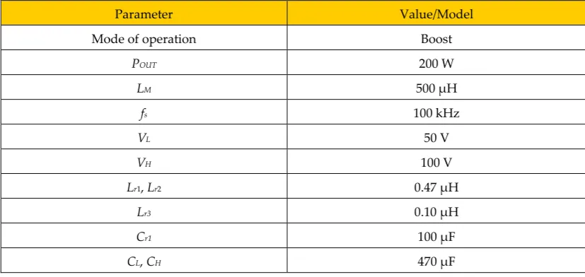
Table 1. Specifications for PSPICE simulation of the prototype converter
Parameter Value/Model
Mode of operation Boost
POUT 200 W
LM 500 µ H
fs 100 kHz
VL 50 V
VH 100 V
Lr1, Lr2 0.47 µ H
Lr3 0.10 µ H
Cr1 100 µ F
2.1. The Hard Switching Mode
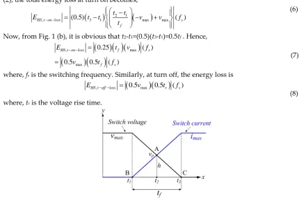
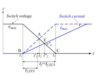
The crossover area that is formed due to the voltage and current rise and fall times (at the switch turn on instant) is shown in Fig. 1. In Fig. 1 (a), the switching waveform pattern for PSPICE simulation is shown to justify the approximation in Fig. 1 (b) for theoretical analysis to be followed. Hence, the
crossover area can be approximated by the area of the triangle ABC
3 1 of ABC (0.5)( )( )
Area = t −t h (1)
Where, (t3-t1) is the base and h is the height of the triangle, respectively. Consequently, for switching frequency fs, the total energy loss at turn on instant is
, (0.5)(3 1)( )( )
HS t on loss s
E − − = t −t h f (2)
It can be assumed that the fall time of the switch voltage (tf) and the rise time of the switch current (tr)
are equal. Hence, (2) can be rewritten as
, (0.5)( )( )( ) HS t on loss f s
E − − = t h f (3)
Now the switch voltage v can be described as
max 1 max f
v v
t t
v
t
−
=
−
−
(4)
where, t1<t<t3. The voltage and the current transients intersect at A located at t2 on the x-axis. Hence,
the voltage v at t2 can be obtained by replacing t=t2 in (4),
2 1
max max
(
)(
)
p f
t
t
v
v
v
t
−
=
−
+
(5)where, vmax is the maximum voltage applied across the switch. Hence, by replicating the concept in
(2), the total energy loss at turn on becomes,
(
)
2 1(
)
, (0.5) 3 1 max max ( )
HS t on loss s
f
t t
E t t v v f
t
− −
−
= − − +
(6)
Now, from Fig. 1 (b), it is obvious that t2-t1=(0.5)(t3-t1)=0.5tf . Hence,
where, fs is the switching frequency. Similarly, at turn off, the energy loss is
(
)(
)
, 0.5 max 0.5 ( )
HS t off loss r s
E − − = v t f
(8) where, tr is the voltage rise time.
Fig. 1. Linearized hard switching (HS) crossover at turn on instant for theoretical analysis
(
)
( )
(
)
(
)
(
)
, max
max
0.25 ( )
0.5 0.5 ( )
HS t on loss f s
f s
E t v f
v t f
− − =
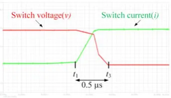
Fig. 2. Simulated waveform at HS turn on instant for the prototype converter
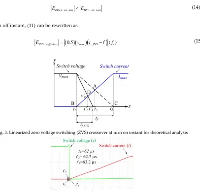
2.2 The Zero Voltage Switching Mode (ZVS)
In this mode, the sharp voltage fall at turn on is restricted by emulating zero voltage across the switch. This is done by turning on the body diode of the switch and discharging the passive snubber element. For computation purpose, it is assumed that the voltage transient is linear. The original hard
switching curve for v is shown by the broken line. Hence, as obvious from Fig. 2 (b) and justifiable
through Fig. 2 (a), the fall time for v is reduced and the voltage-current intersection is shifted left to a new position D from the hard switching point at A. The new intersection point D is located in between
t2 and t1 and let it is at t′2. Consequently, the switch voltage v can be expressed as
max 1 1
max 2 1 f ZVS,
v v
t t
t t
v
t
t
t
−
=
−
=
−
−
−
(9)
where, t1<t<t′3 . If voltage is v′p at t′2, then from (9) it can be obtained as
2 1
max max 3 1
( )( )
p
t t
v v v
t t
−
= − +
−
(10)
Consequently, the energy loss in the ZVS turn on can be derived from (1) as
( )(
)
(
)
( )
(
)
(
)
( )(
)
(
)
2 1
, 3 1 max max
3 1
2 1
, max max
,
max , 2 1
0.5 ( )
0.5 ( )
0.5 ( )
ZVS t on loss s
f ZVS s
f ZVS
f ZVS s
t t
E t t v v f
t t
t t
t v v f
t
v t t t f
− −
−
= − − − +
−
= − +
= − − −
(11)
where, tf, ZVS is the revised switch voltage fall time for the ZVS mode and t′3-t1=tf, ZVS. If t′2-t1=t′, then
(9) becomes
( )(
)
(
)
, 0.5 max , ( )
ZVS t on loss f ZVS s
E − − = v t −t f (12)
Now, geometrically to maintain the ZVS mode switching, the following inequality must be true.
The smaller the value of (tf, ZVS-t′), the better the ZVS execution. Hence, from (7) , (12) and (13), it can be deduced that the energy loss in the ZVS mode is reduced as compared to that in the hard switching counterpart. That is,
, ,
ZVS t on loss HS t on loss
E − − E − − (14)
For turn off instant, (11) can be rewritten as
( )(
)
(
)
, 0.5 max , ( )
ZVS t off loss r ZVS s
E − − = v t −t f (15)
Fig. 3. Linearized zero voltage switching (ZVS) crossover at turn on instant for theoretical analysis
Fig. 4. Simulated waveform at the ZVS mode at turn on instant for the prototype converter
2.3 The Zero Current Switching Mode
In contrary to voltage restriction, the ZCS applies current restriction techniques to reduce the crossover area. For this purpose, the current slope is minimized while the voltage transient remains similar as that in hard switching mode. This is shown in Fig. 3. As evident from Fig. 3 (a), the current rise time (tr) and the voltage fall time (tf) are different for the ZCS operation. Accordingly, the switch voltage v in Fig. 3 (b) can be derived as
max 1 max f
v v
t t
v
t
−
=
−
−
(16)
where, t1<t<t3 . The voltage and current intersection now shift to the right from A to E located at t′′2
on the x-axis. Hence, v′′p at t′′2 can be defined as
2 1
max max 3 1
( )( )
p
t t
v v v
t t
−
= − +
−
(17)
( )(
)
(
)
( )
( )
( )
(
)
( )
( )(
)
(
)
( )
2 1
, 3 1 max max
3 1
2 1
max
max 2 1
0.5
0.5 1
0.5
ZCS t on loss s
f s
f
f s
t t
E t t v v f
t t
t t
t v f
t
v t t t f
− −
−
= − − − +
−
= −
= − −
(18)
Here, t3-t1=tf=tf,ZCS. Now, as E is located far right to the point A in the ZCS operation as obvious from
Fig. 3, the following inequality must be true.
(
t2 − t1)
(
0.5tf)
(19)Consequently,
(
)
tf − t2−t1
(
0.5tf)
(20)
Hence, from (7) and (18), it can be deduced that,
, ,
ZCS t on loss HS t on loss
E − − E − − (21)
That is, the energy loss is reduced in the ZCS mode as compared to the hard switching counterpart. At turn off (18) becomes,
( )(
)
(
)
( )
, 0.5 max 2 1
ZCS t on loss r s
E − − = v t − t−t f (22)
By replacing the parameter values from Fig. 3 (a), the energy loss amounts to
(
)(
)
, 0.5 50 0.5 2.5 6 (100 3) 3.125 ZCS t on loss
E − − = e− e = W
Fig. 5. Linearized zero current switching (ZCS) crossover at turn on instant for theoretical analysis
Fig. 6. Simulated waveform at the ZCS mode turn on instant for the prototype converter
2.4 The True Zero Voltage Zero Current Switching
point move to F to the left of E. This point is located at t′′′2 on the x-axis which is different from the
ZVS intersection point located at t′2. The switch voltage v can be defined as
(
) (
)
1
max max 3 1
t t
v v v
t t − = − + − (23)
where, t1<t<t′3 . Now, v′′′p at t′′′2 can be defined as 2 1 max max 3 1 ( )( ) p t t
v v v
t t
−
= − +
−
(24)
Consequently, the energy loss can be defined as
( )
(
)
(
)
(
)
(
)
(
) (
)
(
)
(
)
(
)
(
)
(
)
2 1
, 3 1 max max
3 1
2 2 2 1
max , , 2 2 max , , max ,
0.5 ( )
0.5 1 ( )
0.5 1 ( )
0.5 ( )
t ZVZCS t on loss s
f ZVS s
f ZVS
f ZVS s
f ZVS
f ZVS s
t t
E t t v v f
t t
t t t t
v t f
t
t t t
v t f
t
v t t x f
− − − − = − − + − − − + − = + − − + = + = − + (25)
Here, t′3-t1=tf,ZVZCS=tf,ZVS and t′2-t1=t′. Moreover, x is defined as
2 2
x=t−t (26)
As F is located at the right of D, x must be positive. Hence, it is obvious from (22) and (25) that the
energy loss in the ZVZCS mode is further truncated as compared to the ZVS or ZCS. For the turn off instant, (26) can be rewritten as
(
)
(
)
, 0.5max , ( )
t ZVZCS t off loss f ZVS s
E− − − = v t − +t x f (27)
Hence, from (7), (11), (18) and (25), it becomes obvious that the ZVZCS mode switching is more efficient in reducing the energy loss at the turn on point than the ZVS or the ZCS. More specifically, as compared to the ZVS, the ZVZCS reduces the loss in percentage by
, , , 2 , 1 100 100
ZVS t on loss ZVZCS t on loss t on loss reduction
ZVS t on loss
f ZVS E E E E t t t − − − − − − − − − − = = + (28)
Roughly the net loss reduction in percentage at the turn on and turn off should be,
2
, 1
1.5
100 total loss reduction
f ZVS t E t t − − = + (29)
As compared to the ZCS, the loss reduction can be defined as
, , , , 2 1 100 100
ZCS t on loss ZVZCS t on loss t on loss reduction
ZCS t on loss f ZVS E E E E t t t − − − − − − − − − − = =
− (30)
Again, the net loss reduction as compared to the ZCS in percentage should be,
,
2 1
1.5
100
f ZVS total loss reduction
By replacing the parameter values from Fig. 8, the energy loss in ZVZCS mode amounts to
(
)(
)
, 0.5 50 0.5 0.7 6 (100 3) 875 ZVZCS t on loss
E − − = e− e = mW
Hence, it can be concluded that the ZVZCS is capable of reducing the energy loss at the switch transition points as compared to that induced in the HS, ZVS or the ZCS mode.
Fig. 7. Linearized zero current switching (ZCS) crossover at turn on instant for theoretical analysis
Fig. 8. Simulated waveform at the ZVZCS mode turn on instant for the prototype converter
3. Analysis for the estimation of the soft switching range
3.1 The Zero Voltage Switching (ZVS)
In the ZVS, the turn on loss is defined in terms of input voltage as
( )(
)
(
)
, 0.5 max , ( )
ZVS t on loss f ZVS s
E − − = v t −t f (32)
Or in terms of switch current, it can be rewritten as
( )(
)( )
(
)
, 0.5 0.25 max , ( )
ZVS t on loss f ZVS s
E − − i t f (33)
It can be observed that the ZVS turn on loss largely depends on the maximum applied switch voltage
vmax which is the input voltage for a forward mode converter. This dependency can be reduced if switching frequency (fs) is decreased. However, it is not an effective solution to reducing the
switching frequency would increase the size of the passive components, while, the term (tf,ZVS-t′) is
3.2 The Zero Current Switching (ZCS)
In the ZCS, the energy loss in terms of maximum switch voltage (vmax) and current (imax) are described
as
( )(
)
(
)
, 0.5 max 2 1 ( )
ZCS t on loss f s
E − − = v t − t−t f (34)
and
( )( )
( )
2, max
4
0.5 ( )
ZCS t on loss f s
t
E i t f
t
− −
(35)
In (34), as obvious from Fig. 3,
(
2 1)
f
t t−t (36)
Hence, the maximum switch voltage (vmax) has minimal effect on the ZCS operation. On the contrary,
the ZCS operation is largely affected by imax as can be seen in (35). To reduce this effect, fs has to be
minimized as the term (t2′′′/t4) is constant. However, as mentioned earlier, it is not an effective solution as the size of the passive components can increase substantially. The dependency on the switch current makes the ZCS operation vulnerable to the converter loading conditions. Consequently, for wide load variation, the ZCS is difficult to achieve. In other words, the soft switching range of operation is affected.
3.3 The True Zero Voltage Zero Current Switching
In this mode, the energy loss terms are
(
)
(
)
(
)
(
)
, max ,
max , 2 1
0.5 ( )
0.5 ( )
t ZVZCS t on loss f ZVS s
f ZVS s
E v t t x f
v t t t f
− − − = − +
= − − (37)
or
(
)
(
)
2, max ,
4
0.5 ( )
t ZVZCS t on loss f ZVS s
t
E i t f
t
− − −
=
(38)
It can be deduced from Fig. 4 that
(
)
, 2 1
f ZVS
t t−t (39)
Hence, it is obvious from (37) that the maximum switch voltage has minimal effect on the true ZVZCS.
Similarly, it can be observed from Fig. 4 that
2 4
t= t (40)
Subsequently, as obvious from (38), the dependency of the ZVZCS operation on the switch current is negligible. Hence, the ZVZCS is not largely affected by the input voltage and loading conditions. In return, it becomes capable of providing wider soft switching range by remaining operational irrespective of the input voltage and load current conditions.
4. Simulation Results for comparative analysis
To prove the theoretical statement, a PSPICE simulation is performed for selected topologies from the recent literature. The converters are simulated in the boost mode and the following specifications are maintained:
Table 2. Common specifications
Parameter Value/Model
Mode of operation Boost
LM 500 µ H
All switches MOSFET IRF150
Furthermore, the converters are intentionally operated at a low power level (i.e. 200 W) for better visualization of the switching losses. The main switches of the converters are taken into consideration to measure the incurred turn on and turn off losses while the converters are operated either in a) the ZVS mode or b) the ZCS mode or c) the ZVZCS mode. The measurement is performed in different states (State A to State F) of the circuit. Each state denotes a unique combination of switching frequency (fs), the input voltage (VL) and the load current. The variation of the operational states makes the results unbiased to the operating conditions of the converter. Furthermore, the measured turn on and turn off losses for different soft switching conditions are averaged out to achieve more accurate results. The simulation results are demonstrated in Table 3 below.
Table 3. Turn on and turn off loss in the main switch State A: fS= 50 kHz, POUT= 200 W, VL=50 V
Refs. for Simulated
topology
Soft switching mode Loss (mW)
Turn on Turn off Turn on Turn off
[4] ZVS ZVS 1200 500
[6] ZVS ZVS 1400 650
[3] ZVS ZVS 1150 520
[1] ZCS ZCS 1480 780
[5] ZCS ZCS 1450 745
[13] ZCS ZCS 1440 745
[2] ZCS ZVS 1390 540
[23] ZVZCS ZVZCS 950 520
[24] ZVZCS ZVZCS 850 440
[25] ZVZCS ZVZCS 820 410
State B: fS= 50 kHz, POUT=200 W, VL=100 V
Simulated topology
Soft switching mode Loss (mW)
Turn on Turn off Turn on Turn off
[4] ZVS ZVS 1350 550
[6] ZVS ZVS 1480 690
[3] ZVS ZVS 1330 560
[1] ZCS ZCS 1405 750
[5] ZCS ZCS 1380 710
[13] ZCS ZCS 1390 725
[2] ZCS ZVS 1340 630
[23] ZVZCS ZVZCS 1080 550
[24] ZVZCS ZVZCS 950 480
[25] ZVZCS ZVZCS 875 355
State C: fS= 50 kHz, POUT=200 W, VL=150 V
Simulated topology
Soft switching mode Loss (mW)
Turn on Turn off Turn on Turn off
[4] ZVS ZVS 1470 620
[6] ZVS ZVS 1540 730
[3] ZVS ZVS 1420 580
[1] ZCS ZCS 1380 720
[5] ZCS ZCS 1305 690
[13] ZCS ZCS 1355 705
[2] ZCS ZVS 1515 695
[24] ZVZCS ZVZCS 880 440
[25] ZVZCS ZVZCS 785 425
State D: fS= 100 kHz, POUT= 200 W, VL=50 V
Simulated topology
Soft switching mode Loss (mW)
Turn on Turn off Turn on Turn off
[4] ZVS ZVS 1750 760
[6] ZVS ZVS 1820 840
[3] ZVS ZVS 1680 740
[1] ZCS ZCS 1850 950
[5] ZCS ZCS 1810 870
[13] ZCS ZCS 1830 840
[2] ZCS ZVS 1840 805
[23] ZVZCS ZVZCS 1345 615
[24] ZVZCS ZVZCS 1285 550
[25] ZVZCS ZVZCS 1270 500
State E: fS= 100 kHz, POUT= 200 W, VL=100 V
Simulated topology
Soft switching mode Loss (mW)
Turn on Turn off Turn on Turn off
[4] ZVS ZVS 1820 810
[6] ZVS ZVS 1880 870
[3] ZVS ZVS 1780 750
[1] ZCS ZCS 1780 920
[5] ZCS ZCS 1785 840
[13] ZCS ZCS 1790 820
[2] ZCS ZVS 1785 850
[23] ZVZCS ZVZCS 1265 675
[24] ZVZCS ZVZCS 1200 590
[25] ZVZCS ZVZCS 1165 525
State F: fS= 100 kHz, POUT= 200 W, VL=150 V
Simulated topology
Soft switching mode Loss (mW)
Turn on Turn off Turn on Turn off
[4] ZVS ZVS 1860 830
[6] ZVS ZVS 1950 920
[3] ZVS ZVS 1805 780
[1] ZCS ZCS 1745 880
[5] ZCS ZCS 1735 800
[13] ZCS ZCS 1755 785
[2] ZCS ZVS 1730 865
[23] ZVZCS ZVZCS 1395 685
[24] ZVZCS ZVZCS 1320 620
[25] ZVZCS ZVZCS 1285 555
To provide a better visual understanding, the average turn on and turn off losses induced in the ZVS, the ZCS or in the ZVZCS mode are plotted in Fig. 5 and 6 respectively at different operational states.
As can be seen, the average turn on loss from State A to State F increases from 1200 mW to 1800 mW,
while the turn off loss increase from 550 mW at State A to 850 mW at State F. For the ZCS, the turn on
loss at State A is 1400 mW which becomes 1700 mW at State F, while it increases from 700 mW to 850
mW at turn off. In contrary, in the ZVZCS mode, the turn on loss is 880 mW at State A which increases
to 1300 mW at State F. Moreover, the turn off loss is 450 mW at State A to 600 mW at State F. On
Fig. 5. Average turn on loss in the main switch
Fig. 6. Average turn off loss in the main switch
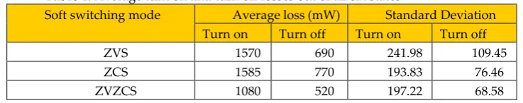
To provide an insight into the soft switching range of operation 1) the average turn on and turn off losses out of all the six states and 2) the cumulated standard deviations from the average values are calculated. The results are shown in Table 4 below. As can be observed, the ZVZCS incurs the lowest turn on and turn off losses on average. Besides, the standard deviation (SD) shows that the deviation from the average is fairly lower for the ZVZCS mode as compared to others. This signifies stable low loss profile throughout all six states and proves the superiority of the ZVZCS soft switching performance in the whole operating range.
Table 4. Average turn on and turn off losses out of all six states
Soft switching mode Average loss (mW) Standard Deviation Turn on Turn off Turn on Turn off
ZVS 1570 690 241.98 109.45
ZCS 1585 770 193.83 76.46
ZVZCS 1080 520 197.22 68.58
5. Experimental verification
To verify the theoretical claim, an experimental test is performed. A prototype ZVZCS converter [22]
states. In this section, the experimental test procedure is discussed. The description of the converter operational modes, intervals and results are to be followed in the rest of this section.
5.1 Converter Topology and PWM Switching
The converter (as shown in Fig. 7) consists of the main switches S1 and S2, the auxiliary switches Sr1
and Sr2, the main inductor LM, the auxiliary inductors Lr1 and Lr2 and the auxiliary capacitor Cr1. It is
bidirectional and operable in the ZVS, the ZCS and the ZVZCS mode separately. For the experimental verification, the converter is tested in the boost mode only and the turn on and turns off losses are
calculated for the main switch S1. For this purpose, the circuit is operated in four different stages,
namely
Stage 1: the ZVZCS mode
Stage 2: the ZVS mode
Stage 3: the ZCS mode and
Stage 4: the hard switching (HS) mode
Fig. 7. The schematic of the ZVZCS converter under test [22]
In Stage 1, the turn on and turn off of S1 is conducted in the ZVZCS mode. To achieve this, both the
auxiliary switches (Sr1 and Sr2) are turned on as shown in Fig. 8 (a). This leads to the near zero
switching loss at the transitions. In Stage 2, Sr1 is turned on and Sr2 is turned off as shown in Fig. 8 (b).
Consequently, S1 is operated in the ZVS mode. The sharp voltage rise across the switch S1 is controlled
by the ZVS mode switching by turning on the respective body diode. In Stage 3, to achieve the ZCS
at S1, the Sr1 is turned off and Sr2 is turned on as in Fig. 8 (c). This forces the body diode of S1 to remain
turned off. Simultaneously, the Lr2 and the capacitor Cr1 realize the ZCS operation in S1. For this
purpose, Lr1 and Lr2 control the sharp rise of current through S1. Finally in Stage 4, for the hard
switching stage, both the auxiliary switches (i.e. Sr1 and Sr2) are turned off as shown in Fig. 8 (d). To
give a general idea on the operation of the circuit, the operational intervals are shortly described next.
(c) (d)
Fig. 8. The PWM switching in (a) Stage 1 (b) Stage 2 (c) Stage 3 (d) Stage 4
5.2 Converter Operational Intervals
The operational intervals are important to understanding the basic operation of the circuit. Hence, the operational intervals are described in short which should be sufficient to understand the soft switching operation.
a) Interval 1 [t1-t0, Stage 1+ Stage 2]:
At t0, the auxiliary switch Sr1 is turned on in the ZVS mode. The current starts to flow through Sr1 and
subsequently charges the resonant inductor Lr3. The capacitor Cr1 turns on the diode Dr and discharges
to the Lr3 through the diode. Throughout this interval, the inductor current iLM remains constant and
discharges to the output. The time interval t10 is determined as
2 3
2 3
10 5 5 5
r r T
S
Lr Lr T
L L L
t
R R R
+ = + =
(41)
b) Interval 2 [t2-t1, Stage 1+ Stage 2]:
At t1, the body diode of S1 is turned on and Lr3 starts to discharge through it. This, in return, enables
S1 to be turned on in the ZVS mode at t2. At t2, the current through the switch Sr1 reaches zero and Sr1
is turned off in ZCS mode. To allow Lr3 to discharge completely, t21 has to be selected as
2 3
2 3
21 3 3 3
r r T
S
Lr Lr T
L L L
t
R R R
+ = + =
(42)
Combining (1) and (2), the following relationship is obtained.
20 8 S
t
(43) Thus, as long as the lower limit restrictions in (1) and (2) are satisfied, the ZVS condition is achievable. However, to avoid unnecessary losses in the auxiliary components and the body diode of the main switch, the delay should be kept equal to or lower than twice the minimum limit. Hence, the functional range of t20 should be
20
16
S t 8
S (44)c) Interval 3 [t3-t2, Stage 1+ Stage 3]:
At t2, the switch S1 is turned on in the ZVZCS mode. To achieve this purpose, the inductor Lr2 in series
with S1, restricts the sharp rise of current through the switch. In general, as the value of the inductor
Lr2 increases, the slope di/dt decreases as obvious from (5). However, excessively large Lr3 would affect the ZVS transition of S1. At t3, Sr2 is turned on for a very short period. Consequently, Cr1 is charged by
the reverse recovery current irr. To this purpose, Cr1 is designed to be able to accommodate the reverse
recovery charge Qrr.
2
2
Lr L
r
di V
dt = L
(45)
d) Interval 4 [t4-t3, Stage 1-4]:
Throughout this interval, the inductor current iLM continues to increase. At t4, S1 is turned off in the
M
L L
M
di V
dt =L
(46)
e) Interval 5 [t5-t4, Stage 1-4]:
This interval is kept short enough to avoid any unnecessary current stress on the power switches and
simultaneously to avoid the short circuit condition while both S1 and S2 are switched on.
f) Interval 6 [t6-t5, Stage 1-4]:
At t6, switch S2 is turned on in the ZVZCS mode. Consequently, the inductor LM starts to discharge
through S2. The inductor current (iLM) decreases as
M
L L H
M
di V V
dt L
−
= (47)
g) Interval 7 [t8-t7, Stage 1-4]:
Throughout this interval, the body diode of S2 remains open. Thus, the inductor LM continues to
discharge through the body diode of the switch S2. At the end of this interval, Sr2 is turned off in the
ZVS mode. iLM decreases as
1 M
L L Cr
M
di V V
dt L
−
= (48)
5.3 Experimental Setup
The prototype circuit is shown in Fig. 9. The circuit is built according to the following specifications:
Table 5. Circuit parameter values
Parameter Value
PO 150 W
LM 1000 µ H
fs 100 kHz
VL 50 V
VH 120 V
Lr1, Lr2 0.47 µ H
Lr3 0.10 µ H
Cr1 100 µ F
CL, CH 470 µ F
The TMS320F2812 DSP is used to generate PWM pulses. The DSP has 12 PWM channels and 150 MHz of clock frequency. Both the high and low voltage side power transistors are implemented with
IPW50R190CE (550 V, 63 A, Rds (on) =190 mΩ) MOSFET. The low power auxiliary switches are
implemented with FDP15N40 (400 V, 15 A, Rds (on) =300 mΩ) MOSFET. The ITECH IT8816B DC
Figure. 9. Experimental prototype circuit
5.4 Results and Discussion
For all cases, the switching losses are measured in switch S1. In Fig. 10, the voltage and current
waveforms of S1 are shown for different switching conditions. The measured losses are given in Table
6. It can be observed from Table 4 that the ZVS and ZCS provide improve the switching states and reduce the losses as compared to the hard switching condition by more than 30 %. However, the improvement induced by the ZVZCS operation from the HS counterpart is more than 80 % which surpasses other soft switching conditions. Thus, the efficiency is largely improved.
(a) (b)
(c) (d)
Figure. 10. Voltage and current waveforms of S1 at the (a) HS (b) ZVS (c) ZCS (d) true ZVZCS conditions
Table 6. Loss in the switch S1
Switching mode
Turn on loss in S1
(mW)
Turn off loss in S1
(mW)
Hard 1600 1850
ZVS 620 400
ZCS 680 480
ZVZCS 160 180
imposed by the ZVZCS operation of the main switch only. Hence, it can be safely concluded that the experimental results are well in accordance with the theoretical claim.
Table 7. Total loss and efficiency drop in S1
Switching mode Total switching loss
(turn on + turn off) in S1
(mW)
Efficiency drop (%)
Hard 3450 2.30
ZVS 1020 0.70
ZCS 320 0.78
ZVZCS 140 0.23
he percentage drop in efficiency imposed by the switch S1 is measured by varying the switching
frequency (fs) and the input voltage (VL) at Stage 1, 2 and 3. For this purpose, the fs is varied from 20
kHz to 150 kHz while VL is kept constant at 80 V and PO=150 W. On the other hand, VL is varied from
20 V to 120 V while fs is kept constant at 100 kHz and PO=150 W. The results are demonstrated in Figs.
11 (a) and (b) respectively. As obvious, the efficiency drop in the ZVZCS mode remains consistently lower and is more stable throughout the operating conditions (i.e. variation in fs and VL). For example,
as can be seen in Fig. 11 (a), Δ Ed= 0.2 % and 0.1 % for the ZVS, ZCS and the ZVZCS respectively.
Similarly, it is 0.15 % and 0.05 % for the ZVS, ZCS and the ZVZCS respectively as shown in Fig. 11 (b). Consequently, wider soft switching operating range in the ZVZCS mode is ensured.
(a) (b)
Figure. 11. Efficiency drop imposed by switch S1 against (a) fs (b) VL
6. Discussion
the incurred turn on and turns off losses in the main switch are measured under these conditions. Overall, it is observed that the ZVZCS mode reduces the switching losses as compared to the HS, the ZVS or the ZCS and help to improve the converter efficiency further. Moreover, it is found that the efficiency drop remains consistently low and stable while measured against the variation of switching frequency and input voltage. This proves the wider operability of the ZVZCS over the ZVS and the ZCS modes.
Author Contributions: 1. Conceptualization, R H ASHIQUE, Z. SALAM; methodology, R H ASHIQUE.; software, ; validation, R H ASHIQUE, Z. SALAM.; formal analysis, R H ASHIQUE, Z. SALAM; investigation, R H ASHIQUE, Z. SALAM.; resources, R H ASHIQUE, Z. SALAM.; data curation; writing—original draft preparation, R H ASHIQUE; writing—review and editing, R H ASHIQUE, Z. SALAM.; visualization; supervision, Z. SALAM. All authors have read and agreed to the published version of the manuscript.”
Conflicts of Interest: The authors declare no conflict of interest.
References
[1] W. Chien-Ming, "A New Family of Zero-Current-Switching (ZCS) PWM Converters," IEEE
Transactions on Industrial Electronics, vol. 52, pp. 1117-1125, 2005.
[2] M. Mohammadi, E. Adib, and M. R. Yazdani, "Family of Soft-Switching Single-Switch PWM Converters With Lossless Passive Snubber," IEEE Transactions on Industrial Electronics, vol. 62, pp. 3473-3481, 2015.
[3] M. R. Mohammadi and H. Farzanehfard, "A New Family of Zero-Voltage-Transition
Nonisolated Bidirectional Converters With Simple Auxiliary Circuit," IEEE Transactions on Industrial
Electronics, vol. 63, pp. 1519-1527, 2016.
[4] S. Dusmez, A. Khaligh, and A. Hasanzadeh, "A Zero-Voltage-Transition Bidirectional DC/DC Converter," Industrial Electronics, IEEE Transactions on, vol. 62, pp. 3152-3162, 2015.
[5] T. Mishima and M. Nakaoka, "A Practical ZCS-PWM Boost DC-DC Converter With
Clamping Diode-Assisted Active Edge-Resonant Cell and Its Extended Topologies," IEEE
Transactions on Industrial Electronics, vol. 60, pp. 2225-2236, 2013.
[6] J. Zhang, J.-S. Lai, R.-Y. Kim, and W. Yu, "High-power density design of a soft-switching high-power bidirectional dc–dc converter," Power Electronics, IEEE Transactions on, vol. 22, pp. 1145-1153, 2007.
[7] R. H. Ashique, Z. Salam, and M. J. A. Aziz, "A high power density soft switching
bidirectional converter using unified resonant circuit," in Energy Conversion (CENCON), 2015 IEEE
Conference on, 2015, pp. 165-170.
[8] D.-W. Han, H.-J. Lee, S.-C. Shin, J.-G. Kim, Y.-c. Jung, and C.-Y. Won, "A new soft switching ZVT boost converter using auxiliary resonant circuit," in Vehicle Power and Propulsion Conference (VPPC), 2012 IEEE, 2012, pp. 1250-1255.
[9] B. Ivanovic and Z. Stojiljkovic, "A novel active soft switching snubber designed for boost converter," IEEE Transactions on Power Electronics, vol. 19, pp. 658-665, 2004.
[10] T. Mishima and M. Nakaoka, "A new family of soft switching PWM non-isolated DC-DC converters with Active auxiliary Edge-Resonant Cell," in Power Electronics Conference (IPEC), 2010 International, 2010, pp. 2804-2809.
[11] D. Patil, A. K. Rathore, and D. Srinivasan, "A non-isolated bidirectional soft switching
current fed LCL resonant dc/dc converter to interface energy storage in DC microgrid," in Applied
Power Electronics Conference and Exposition (APEC), 2015 IEEE, 2015, pp. 709-716.
[12] A. K. Rathore, D. R. Patil, and D. Srinivasan, "A Non-Isolated Bidirectional Soft Switching
Current fed LCL Resonant DC/DC Converter to Interface Energy Storage in DC Microgrid," Industry
[13] M. Ahmadi, M. R. Mohammadi, E. Adib, and H. Farzanehfard, "Family of non-isolated zero
current transition bi-directional converters with one auxiliary switch," IET Power Electronics, vol. 5,
pp. 158-165, 2012.
[14] H. Ardi, R. R. Ahrabi, and S. N. Ravadanegh, "Non-isolated bidirectional DC–DC converter
analysis and implementation," IET Power Electronics, vol. 7, pp. 3033-3044, 2014.
[15] E. Sanchis-Kilders, A. Ferreres, E. Maset, J. B. Ejea, V. Esteve, J. Jordan, et al., "Bidirectional high-power high-efficiency non-isolated step-up dc-dc converter," in Power Electronics Specialists Conference, 2006. PESC'06. 37th IEEE, 2006, pp. 1-7.
[16] B. Akin, "An Improved ZVT–ZCT PWM DC–DC Boost Converter With Increased Efficiency," Power Electronics, IEEE Transactions on, vol. 29, pp. 1919-1926, 2014.
[17] I. Aksoy, H. Bodur, and A. F. Bakan, "A New ZVT-ZCT-PWM DC–DC Converter,"
IEEE Transactions on Power Electronics, vol. 25, pp. 2093-2105, 2010.
[18] H. Bodur and A. F. Bakan, "A new ZVT-ZCT-PWM DC-DC converter," Power Electronics,
IEEE Transactions on, vol. 19, pp. 676-684, 2004.
[19] H. Bodur and A. F. Bakan, "A new ZVT-ZCT-PWM DC-DC converter," IEEE Transactions on
Power Electronics, vol. 19, pp. 676-684, 2004.
[20] C. M. de Oliveira Stein and H. L. Hey, "A true ZCZVT commutation cell for PWM converters," Power Electronics, IEEE Transactions on, vol. 15, pp. 185-193, 2000.
[21] S. Urgun, "Zero-voltage transition–zero-current transition pulsewidth modulation DC–DC buck converter with zero-voltage switching‣zero-current switching auxiliary circuit," Power Electronics, IET, vol. 5, pp. 627-634, 2012.
[22] R. H. Ashique and Z. Salam, "A Family of True Zero Voltage Zero Current Switching
(ZVZCS) Non-isolated Bidirectional DC-DC Converter with Wide Soft Switching Range," IEEE
Transactions on Industrial Electronics, vol. PP, pp. 1-1, 2017.
[23] C. d. O. Stein and H. L. Hey, "A true ZCZVT commutation cell for PWM converters," in
Applied Power Electronics Conference and Exposition, 1998. APEC'98. Conference Proceedings 1998., Thirteenth Annual, 1998, pp. 1070-1076.
[24] B. Akın, "An improved ZVT–ZCT PWM DC–DC boost converter with increased efficiency,"
IEEE Transactions on Power Electronics, vol. 29, pp. 1919-1926, 2014.