Article
1
Enhanced Thermoelectric Conversion Efficiency of
2
CVD Graphene with Reduced Grain Sizes
3
Gyumin Lim 1, Kenneth David Kihm 2,*, Hong Goo Kim 1, Woorim Lee 1, Woomin Lee 1, Kyung
4
Rok Pyun 1, Sosan Cheon 1, Phillip Lee 3, Jin Young Min 4 and Seung Hwan Ko 1
5
1 School of Mechanical and Aerospace Engineering, Seoul National University, Seoul 08826, South Korea;
6
7
2 Mechanical, Aerospace, and Biomedical Engineering, University of Tennessee, Knoxville, Tennessee 37996,
8
USA; [email protected]
9
3 Korea Institute of Science and Technology, Seoul 02792, South Korea; [email protected]
10
4 School of Mechanical Engineering, Korea University, Seoul 02841, South Korea; [email protected]
11
* Correspondence: [email protected]; Tel.: +1-865-974-5292
12
13
Abstract: The grain size of CVD (Chemical Vapor Deposition) graphene was controlled by changing
14
the precursor gas flow rates, operation temperature, and chamber pressure. Graphene of average
15
grain sizes of 4.1 µm, 2.2 µm, and 0.5 µm were synthesized in high quality and full coverage. The
16
possibility to tailor the thermoelectric conversion characteristics of graphene has been exhibited by
17
examining the grain size effect on the three elementary thermal and electrical properties of , S, and
18
k. Electrical conductivity () and Seebeck coefficients (S) were measured in a vacuum for supported
19
graphene on SiO2/Si FET (Field Effect Transistor) substrates so that the charge carrier density could
20
be changed by applying a gate voltage ( ). Mobility (µ) values of 529~1042, 459~745, and 314~490
21
cm2/V·s for the three grain sizes of 4.1 µm, 2.2 µm, and 0.5 µm, respectively, were obtained from the
22
slopes of the measured vs. graphs. The power factor (PF), the electrical portion of the
23
thermoelectric figure of merit (ZT), decreased by about one half as the grain size was decreased,
24
while the thermal conductivity (k) decreased by one quarter for the same grain decrease.Finally, the
25
resulting ZT increased more than two times when the grain size was reduced from 4.1 µm to 0.5
26
µm.
27
Keywords: Thermoelectric conversion efficiency; CVD graphene; Grain sizes; FET 4-point
28
measurements; Electrical conductivity; Seebeck coefficient.
29
30
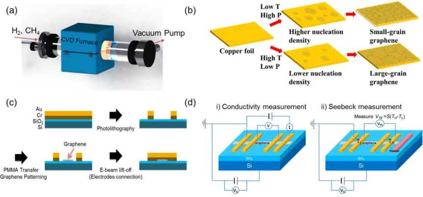
1. Introduction
31
The thermoelectric effect enables direct energy conversions between temperature and electric
32
voltage differences. When a temperature gradient is applied, the momentum difference between
33
charge carriers causes them to shift to one side, yielding voltage potential inside the materials. Since
34
it allows for the conversion of wasted heat into electrical energy, having control over the
35
thermoelectric effect would give rise to one of the most promising sources of renewable energy;
36
because the eco-friendly generation of electrical energy only requires a temperature difference to
37
reuse the wasted heat energy.
38
Graphene has high potential for becoming a thermoelectric material due to its high electrical
39
properties. Its high thermal conductivity, however, has prevented graphene from being used as a
40
thermoelectric material in reality. In order to enhance graphene's thermoelectric properties, many
41
ideas have been proposed aimed at lowering its thermal conductivity, including defect controlling
42
[1] and management of grain size [2,3]. Among the various proposals, controlling grain size seems to
43
be a highly viable way to handle the carriers’scattering of graphene because it does not add artificial
44
knowledge, thus far no study has attempted to characterize the figure of merit (ZT = ) for
46
graphene with controlled grain sizes. In our previous study, we have experimentally verified a
47
decrement of thermal conductivity by controlling the polycrystalline graphene domain sizes [2],
48
which can lead to the possibility of ZT enhancement of CVD graphene.
49
In this paper, as there is still a need for examining the ZT values, we focus on measuring both
50
the electrical conductivity () and the Seebeck coefficients (S). Graphene was synthesized on Cu foil
51
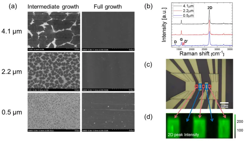
by using the LPCVD (Low Pressure Chemical Vapor Deposition) method, which allows for the
52
control of the grain sizes, and then subsequently transferred onto a SiO2/Si (450 nm/525 µm) FET
53
substrate. The electrical properties ( and S) of graphene were measured using the four-point
54
technique for three different grain sizes of 0.5 µm, 2.2 µm, and 4.1 µm, while the charge carrier density
55
was controlled by varying the gate voltage levels.
56
2. Materials and Methods
57
Graphene was synthesized from the CVD system by ScienTech Inc. (Figure 1a), where CH4 was
58
used as the carbon source and H2 was used to dissociate H atoms upon their detachment from CH4
59
as well as to ensure a single layer by etching away any multiple layers of graphene. The 25 µm-thick
60
Cu foil with 99.999% purity (Alfa Aesar Inc.) was used as both a catalyst and substrate. The grain size
61
of graphene was controlled by comprehensively changing the CH4 to H2 ratio, temperature (T), and
62
pressure (P) of the chamber. Details of the synthesis conditions are shown in Table 1.
63
64
Figure 1. (a) Schematic of CVD graphene synthesis system (b) Grain size control by synthesis
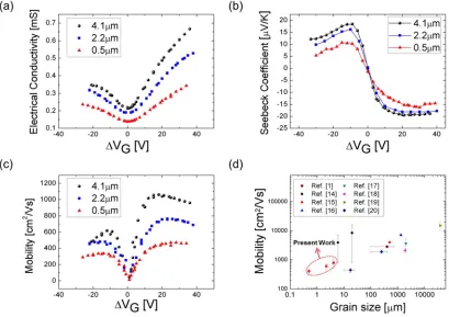
65
temperature and pressure variations (c) Fabrication process diagram for the Field Effect Transistor
66
(FET) substrate with electrode/graphene sample laid down (d) Schematic of the 4-point
67
measurement layout
68
Table 1. CVD graphene synthesis conditions for three different grain sizes
69
Grain Size [µm] 4.1 2.2 0.5
Temperature [℃] 1000 900 800
Pressure [Torr] Step 1 Step 2 Step 1 Step 2 1.09
0.19 0.30 0.37 1.08
Gas flow rate ratio CH4:H2
[sccm:sccm] 30:5 60:5 80:5 200:100 200:100
CVD graphene with smaller grain sizes was synthesized at low T and under high P to make the
70
nucleation density higher, whereas graphene with larger grain sizes was synthesized at high T and
71
low P to make the nucleation density lower, as depicted in Figure 1b. For both the 4.1 µm and 2.2 µm
72
graphene samples, graphene was synthesized following a two-step process: first, flow rates for CH4
73
and H2 were set relatively low so that graphene could grow slowly with enlarged grain sizes; second,
74
the gas flow rates were set high in order to supply enough of a carbon source to ensure the full
75
coverage of graphene. For the 0.5 µm graphene, it was synthesized in a single step with high gas flow
76
rates so that the graphene would grow rapidly while the grain size stayed small. This also enabled
77
full coverage of graphene.
78
The FET substrate was fabricated through lithography, as schematically shown in Figure 1c. It
79
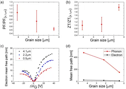
was designed to measure electrical conductivity and Seebeck coefficients in the same substrate by
80
using a micro-heater and electrodes to detect electrical potentials. The micro-heater/electrodes were
81
made of 200 nm thick Au laid on a 20 nm thick Cr contact layer, which were patterned through
82
photolithography on a Si substrate with a thermally oxidized 450-nm thick SiO2 layer on the top
83
surface. Graphene was patterned between the electrodes via photolithography, and the electrodes
84
were connected above the graphene through e-beam lithography.
85
The 4-point measurement (Figure 1d) is an electrical measuring technique that uses separate
86
pairs of current-carrying and voltage-sensing electrodes to make more accurate measurements, as
87
compared to the conventional two-point sensing. The key advantage of the 4-point method is that the
88
separation of current- and voltage-electrodes eliminates the errors caused by the wiring and contact
89
resistances.
90
After fabricating the FET substrates, graphene was transferred onto it using the well-established
91
PMMA method. CVD graphene is naturally p-doped upon the exposure to the oxygen and hydrogen
92
atoms in air. Since we wanted to observe the Dirac point, we needed to minimize the p-doping effect
93
by means of vacuum annealing. Annealing under excessively high temperature and/or overly long
94
duration is known to attach graphene to the substrate too strongly, so much so that it degrades the
95
quality of graphene [4-6]. Accordingly, we opted to anneal graphene only for 2 hours at 250℃ so that
96
the p-doping effect would be sufficiently reduced without degrading the graphene sample.
97
The SEM image was taken once during the intermediate growth of grains and again after the full
98
growth on the Cu foil (Figure 2a). The less dense seeding of graphene provides bigger graphene
99
islands that eventually grow into larger grains. Mild dry annealing was used to oxidize Cu foils along
100
the grain boundaries to identify grain sizes of fully grown graphene [2]. We conducted the digital
101
image processing to enhance the contrast of optical images, where the total graphene area was
102
divided by the total number of grains to determine the average grain sizes of the three tested samples:
103
4.1 µm, 2.2 µm, and 0.5 µm. The 2D and G peaks in the Raman spectra (Figure 2b) are located near
104
2700 and 1600 cm-1, respectively, and the 2D/G peak ratio is greater than two for all three samples,
105
indicating that high quality single layer graphene was properly transferred onto the SiO2/Si substrate
106
[7-11]. For the sample with the smallest grain size, the D peak starts to appear due to the enhanced
107
defects or atomic irregularities associated with the increased grain boundaries. The D/D’ peak
108
intensity ratio of about 3.5 also implies that the D peak appearance can be attributed to the boundary
109
defects [12]. In Figure 2c, the microscopic image indicates the well-fabricated FET 4-point electrodes.
110
The 2D peak Raman mapping (Figure 2d) exhibits the uniform 2D peak intensity distribution in the
111
exposed graphene area marked in green (corresponding to the red circles in Figure 2c), whereas the
112
alternative areas marked in black (corresponding to the blue squares) do not show any intense 2D
113
peaks due to the Au electrodes’ coverage over the graphene. The uniform 2D peak intensity at the
114
exposed graphene areas between the electrodes confirms the continuous and uniform-quality of the
115
117
118
Figure 2. (a) SEM images of graphene growth on Cu foil for three different grain sizes. (b) Raman
119
spectra of graphene samples laid on the FET substrate. (c) Optical image of the 4-point electrodes
120
with graphene sample integrated. (d) 2D peak Raman mapping of graphene to distinguish the
121
exposed graphene regions (green) from the electrode-covered regions (black).
122
3. Results and Discussion
123
The measured electrical conductivities ( ) and Seebeck coefficients (S) are shown in Figures 3a
124
and 3b, respectively. Both graphs are plotted with respect to ∆ ( − , , where is the
125
gate voltage applied and , is the gate voltage at the Dirac point). The corresponding absolute
126
maximum values of the Seebeck coefficient were about 19.5 µV/K, 18.2 µV/K, and 16.2 µV/K (Fig 3b),
127
respectively, in a positive ∆ range. The electrical mobility (µ) of graphene (Figure 3c) was then
128
determined from the slope of the electrical conductivity, which is given by:
129
( ) = − , + , (1)
where σ is the electrical conductivity, W and L are the width and the length of graphene, respectively,
130
is the substrate’s capacity, and µ is the electrical mobility [13]. Mobility values obtained as
131
functions of gate voltage were used to get the electron MFP (Mean Free Path) in Figure 4c. Effective
132
mobility values of graphene were measured to be 529~1042 cm2/V·s, 459~745 cm2/V·s, and 314~490
133
cm2/V·s for the grain sizes of 4.1 µm, 2.2 µm, and 0.5 µm, respectively. Measured mobility data for
134
relatively larger grains by other research groups [1,14-20] are also shown in Figure 3d. A gradual
135
increase of the electrical mobility is shown with increasing grain sizes, at the ratio of one
order-of-136
magnitude increase of mobility to nearly four orders-of-magnitude increase of the grain size.
137
Previously published Seebeck coefficient data are summarized in Table 2 [1,21-28]. Although the
138
grain size effect on the Seebeck coefficients were not examined in these studies, the reported data
139
ranges from 10 to 100 µV/K, depending on different graphene sample preparations and
post-140
treatments. It is known that the residual carrier density induced by charged impurities has significant
141
effects on Seebeck coefficients near the Dirac point, thus consequently affecting the maximum values
142
of Seebeck coefficients [29]. This also implies that inherent charged impurities induced during the
143
fabrication process can result in variations of measured Seebeck coefficients. Our measured range of
144
Seebeck coefficients of 16~20 µV/K is smaller than the 55 µV/K measured for the case of the 300 µm
145
147
148
Figure 3. (a) Electrical conductivity for the three grain sizes of 4.1 µm, 2.2 µm, and 0.5 µm as functions
149
of the gate voltage sweep. (b) Seebeck coefficient for the three grain sizes as functions of the gate
150
voltage sweep. (c) Mobility for the three grain sizes as functions of the gate voltage. (d) Measured
151
mobility data compared with published data for varied grain sizes.
152
153
Table 2. Published list of Seebeck coefficients of CVD graphene
154
(Note: The grain size dependence of Seebeck coefficients is unavailable from any of these studies.)
155
156
Reference Published year
Grain size Seebeck Coefficient
Descriptions
Ref. [22] 2010 - ~9 µV/K @ 300 K Linear dependence of S on T for 50<T<300K
Ref. [23] 2011 - ~50 µV/K @ 500K
~30 µV/K @ 300K
Sensitivity of S to the surface charge doping by exposure to the air, N2O, and NH3
Ref. [24] 2013 - ~10 µV/K @ 300K Linear dependence of S and electrical conductivity
on T for 75<T<300K
Ref. [25] 2014 - ~20 µV/K @ 150K Observation on the large fluctuation of S near the
Dirac point associated with the disorder in graphene at high magnetic field & low temperature
Ref. [26] 2015 - ~100 µV/K @ 300K N-type doping of CVD graphene by H2 exposure
verified by S measurement
Ref. [1] 2017 Average 300
µm(100-700)
~55 µV/K @ RT ZT enhancement using O2 plasma
irradiation.(ZT/ZT0 ~ 3)
Ref. [28] 2018 - ~30 µV/K @ RT Estimation of electrical conductivity and Seebeck of
graphene sheet and graphene nanoribbon by experimental and theoretical approach
157
The thermoelectric figure-of-merit (ZT = ) is determined from the presently measured , S,
158
group’s previous report, as 2660, 1890, and 680 W/m·K for grain sizes 4.1 µm, 2.2 µm, and 0.5 µm,
160
respectively[2]. The normalized power factor (PF = , Figure 4a) shows a slower decrease with
161
decreasing grain size than the corresponding k decrease: the PF decreases to 1/2 while k decreases to
162
1/4. Consequently, when the grain size is reduced from 4.1 µm to 0.5 µm, the ZT value (Figure 4b)
163
increases by approximately two times. The corresponding ZT values are 0.55 × 10⁻⁴, 0.58 × 10⁻⁴, and
164
1.13 × 10⁻⁴ at room temperature (T = 300K). The detrimental effect of the grain size on k becomes more
165
significant when the grain size is comparable to the phonon mean-free-path (MFP) of about 800 nm
166
[2]. Also, shows a predominantly decreasing pattern for grain sizes smaller than 800 nm [3]. In
167
other words, the grain size effect on ZT is less pronounced when the grain sizes are 4.1 µm or 2.2 µm,
168
but shows a dramatic increase for the sub-micron grain size of 0.5 µm. The rms error bars with 95%
169
confidence intervals account for the 5-10 measurement samples for each grain size.
170
171
172
Figure 4. (a) Power Factor dependence on the grain sizes of graphene. (b) Gradually increasing ZT
173
with decreasing grain sizes. (c) Electron mean free path as a function of gate voltage for the graphene
174
of grain sizes 4.1 µm, 2.2 µm, and 0.5 µm. (d) Phonon and electron mean free path of graphene of
175
grain sizes 4.1 µm, 2.2 µm, and 0.5 µm.
176
177
It is well known that the electron scattering increment at the grain boundaries reduces the
178
electrical transport and properties [14,20,30]. The electron MFP (Figure 4c) is given by [31,32], =
179
( ) , where h is Planck’s constant, e is the elementary charge, µ is the electrical mobility, and n is
180
the charge carrier density. The estimated electron MFPs converge to 24.9 nm, 19.1 nm, and 12.5 nm
181
for the grain sizes of 4.1 µm, 2.2 µm, and the 0.5, respectively (Figure 4d). The decrements in the 2.2
182
µm and the 0.5 µm samples were 23.3% and 49.8%, respectively, relative to the 4.1 µm sample. The
183
electron MFPs were reported to be in the range from 10 to 100 nm for the charge carrier density range
184
of 1012~1013 cm-2, which corresponds to the gate voltage range larger than 13 V [33].
185
In contrast, the phonon MFP is given by a Landauer-like approach [34,35], ( ) =
186
+ , where Gball is the ballistic thermal conductance (~4.2 × 10⁹ W/m2K at room
187
temperature), lG is the grain size, and λ is the phonon MFP. The estimated phonon MFP’s are 476.9
188
The decrements in the 2.1 µm and 0.5 µm samples were 24.5% and 68.0%, respectively, from the 4.1
190
µm sample. The larger decrements of the phonon MFPs than the electron MFPs shows consistency
191
with the idea that decreasing grain size is more effective for enhancing the scattering rate of phonons
192
than that of electrons. This is the possible reason why graphene of reduced grain sizes shows less
193
decrement for electrical properties than for thermal conductivity, and thus results in an increased ZT.
194
4. Conclusions
195
We investigated the dependence of the thermoelectric figure of merit, ZT, on the grain size of
196
CVD graphene. Electrical conductivity () and Seebeck coefficients (S) were measured for three
197
different grain sizes: 4.1, 2.2, and 0.5 µm using a FET 4-point measurement technique. Since the
198
decrement of the corresponding thermal conductivity (k) was larger than the decrement of the PF,
199
more than two times the original ZT value was observed as the grain size was decreased from 4.1 µm
200
to 0.5 µm. We have shown the possibility that ZT can be tailored by altering the grain size of
201
graphene, which is a crucial factor in CVD graphene synthesis. Furthermore, this enhancement of the
202
thermoelectric properties opens the possibility of graphene to be considered as a more realistic
203
thermoelectric material.
204
205
Author Contributions: G.L. and K.D.K. carried out experiments including graphene synthesis, FET fabrication,
206
transfer, and measurements and wrote this paper; H.G.K., W.R.L., and W.M.L. contributed to CVD graphene
207
synthesis, and together with K.P., helped to transfer graphene onto the FET electrodes and developed the
208
electrical properties measurements system; H.G.K. and S.C. conducted work on the theoretical aspects of the
209
manuscript; P.L. and J.M. contributed to fabricate FET substrates; S.K. advised the experimental layouts and had
210
discussions to elaborate the experimental results.
211
Acknowledgments: This research was primarily supported by the Nano-Material Technology Development
212
Program (R2011-003-2009) and Magnavox Professorship fund (R0-1137-3164) from the University of Tennessee.
213
Conflicts of Interest: The authors declare no conflict of interest.
214
References
215
1. Yuki, A.; Yuki, I.; Kuniharu, T.; Seiji, A.; Takayuki, A. Enhancement of graphene thermoelectric performance
216
through defect engineering. 2D Mater. 2017, 4, 025019.
217
2. Lee, W.; Kihm, K.D.; Kim, H.G.; Shin, S.; Lee, C.; Park, J.S.; Cheon, S.; Kwon, O.M.; Lim, G.; Lee, W. In-Plane
218
Thermal Conductivity of Polycrystalline Chemical Vapor Deposition Graphene with Controlled Grain Sizes.
219
Nano Lett. 2017, 17, 2361-2366.
220
3. Ma, T.; Liu, Z.; Wen, J.; Gao, Y.; Ren, X.; Chen, H.; Jin, C.; Ma, X.-L.; Xu, N.; Cheng, H.-M.; Ren, W. Tailoring
221
the thermal and electrical transport properties of graphene films by grain size engineering. Nat. Commun. 2017,
222
8, 14486.
223
4. Cheng, Z.; Zhou, Q.; Wang, C.; Li, Q.; Wang, C.; Fang, Y. Toward Intrinsic Graphene Surfaces: A Systematic
224
Study on Thermal Annealing and Wet-Chemical Treatment of SiO2-Supported Graphene Devices. Nano Lett.
225
2011, 11, 767-771.
226
5. Pirkle, A.; Chan, J.; Venugopal, A.; Hinojos, D.; Magnuson, C.W.; McDonnell, S.; Colombo, L.; Vogel, E.M.;
227
Ruoff, R.S.; Wallace, R.M. The effect of chemical residues on the physical and electrical properties of chemical
228
vapor deposited graphene transferred to SiO2. Appl. Phys. Lett. 2011, 99, 122108.
229
6. Lin, Y.-C.; Lu, C.-C.; Yeh, C.-H.; Jin, C.; Suenaga, K.; Chiu, P.-W. Graphene Annealing: How Clean Can It Be?
230
Nano Lett. 2012, 12, 414-419.
231
7. Ferrari, A.C. Raman spectroscopy of graphene and graphite: Disorder, electron–phonon coupling, doping and
232
8. Basko, D.M.; Piscanec, S.; Ferrari, A.C. Electron-electron interactions and doping dependence of the
two-234
phonon Raman intensity in graphene. Phys. Rev. B. 2009, 80, 165413.
235
9. Venezuela, P.; Lazzeri, M.; Mauri, F. Theory of double-resonant Raman spectra in graphene: Intensity and line
236
shape of defect-induced and two-phonon bands. Phys. Rev. B. 2011, 84, 035433.
237
10. Ferrari, A.C.; Basko, D.M. Raman spectroscopy as a versatile tool for studying the properties of graphene.
238
Nat. Nanotechnol. 2013, 8, 235.
239
11. Lee, W.; Kihm, K.D.; Kim, H.G.; Lee, W.; Cheon, S.; Yeom, S.; Lim, G.; Pyun, K.R.; Ko, S.H.; Shin, S. Two
240
orders of magnitude suppression of graphene's thermal conductivity by heavy dopant (Si). Carbon. 2018.
241
12. Eckmann, A.; Felten, A.; Mishchenko, A.; Britnell, L.; Krupke, R.; Novoselov, K.S.; Casiraghi, C. Probing the
242
Nature of Defects in Graphene by Raman Spectroscopy. Nano Lett. 2012, 12, 3925-3930.
243
13. Chen, J.H.; Jang, C.; Adam, S.; Fuhrer, M.S.; Williams, E.D.; Ishigami, M. Charged-impurity scattering in
244
graphene. Nat. Phys. 2008, 4, 377.
245
14. Li, X.; Magnuson, C.W.; Venugopal, A.; An, J.; Suk, J.W.; Han, B.; Borysiak, M.; Cai, W.; Velamakanni, A.;
246
Zhu, Y.; Fu, L.; Vogel, E.M.; Voelkl, E.; Colombo, L.; Ruoff, R.S. Graphene Films with Large Domain Size by a
247
Two-Step Chemical Vapor Deposition Process. Nano Lett. 2010, 10, 4328-4334.
248
15. Li, X.; Magnuson, C.W.; Venugopal, A.; Tromp, R.M.; Hannon, J.B.; Vogel, E.M.; Colombo, L.; Ruoff, R.S.
249
Large-Area Graphene Single Crystals Grown by Low-Pressure Chemical Vapor Deposition of Methane on
250
Copper. J. Am. Chem. Soc. 2011, 133, 2816-2819.
251
16. Gao, L.; Ren, W.; Xu, H.; Jin, L.; Wang, Z.; Ma, T.; Ma, L.-P.; Zhang, Z.; Fu, Q.; Peng, L.-M.; Bao, X.; Cheng,
252
H.-M. Repeated growth and bubbling transfer of graphene with millimetre-size single-crystal grains using
253
platinum. Nat. Commun. 2012, 3, 699.
254
17. Shanshan, C.; Hengxing, J.; Harry, C.; Qiongyu, L.; Hongyang, L.; Won, S.J.; Richard, P.; Lei, L.; Weiwei, C.;
255
S., R.R. Millimeter-Size Single-Crystal Graphene by Suppressing Evaporative Loss of Cu During Low Pressure
256
Chemical Vapor Deposition. Adv. Mat. 2013, 25, 2062-2065.
257
18. Wang, C.; Chen, W.; Han, C.; Wang, G.; Tang, B.; Tang, C.; Wang, Y.; Zou, W.; Chen, W.; Zhang, X.-A.; Qin,
258
S.; Chang, S.; Wang, L. Growth of Millimeter-Size Single Crystal Graphene on Cu Foils by Circumfluence
259
Chemical Vapor Deposition. Sci. Rep. 2014, 4, 4537.
260
19. Wu, T.; Zhang, X.; Yuan, Q.; Xue, J.; Lu, G.; Liu, Z.; Wang, H.; Wang, H.; Ding, F.; Yu, Q.; Xie, X.; Jiang, M.
261
Fast growth of inch-sized single-crystalline graphene from a controlled single nucleus on Cu–Ni alloys. Nat.
262
Mater. 2015, 15, 43.
263
20. A., V.V.Z.; A., A.W.J.; A., S.A.; Philipp, B.W.; Stephan, H. Electronic properties of CVD graphene: The role of
264
grain boundaries, atmospheric doping, and encapsulation by ALD. Phys. Status Solidi B. 2016, 253, 2321-2325.
265
21. Bao, W.S.; Liu, S.Y.; Lei, X.L. Thermoelectric power in graphene. J. Phys.: Condens. Matter. 2010, 22, 315502.
266
22. Xu, X.; Wang, Y.; Zhang, K.; Zhao, X.; Bae, S.; Heinrich, M.; Bui, C. T.; Xie, R.; Thong, J. T. L.; Hong, B. H.;
267
Loh, K. P.; Li, B.; Oezyilmaz, B. arXiv: 1012.2937[cond-mat.mes-hall], (accessed Dec 14, 2010).
268
23. Sidorov, A.N.; Sherehiy, A.; Jayasinghe, R.; Stallard, R.; Benjamin, D.K.; Yu, Q.; Liu, Z.; Wu, W.; Cao, H.;
269
Chen, Y.P.; Jiang, Z.; Sumanasekera, G.U. Thermoelectric power of graphene as surface charge doping indicator.
270
Appl. Phys. Lett. 2011, 99, 013115.
271
24. Babichev, A.V.; Gasumyants, V.E.; Butko, V.Y. Resistivity and thermopower of graphene made by chemical
272
vapor deposition technique. J. Appl. Phys. 2013, 113, 076101.
273
25. Nam, Y.; Sun, J.; Lindvall, N.; Yang, S.J.; Park, C.R.; Park, Y.W.; Yurgens, A. Unusual thermopower of
274
26. Hong, S.J.; Park, M.; Kang, H.; Lee, M.; Soler-Delgado, D.; Shin, D.S.; Kim, K.H.; Kubatkin, S.; Jeong, D.H.;
276
Park, Y.W.; Kim, B.H. Verification of electron doping in single-layer graphene due to H2 exposure with
277
thermoelectric power. Appl. Phys. Lett. 2015, 106, 142110.
278
27. Amollo, T.A.; Mola, G.T.; Kirui, M.S.K.; Nyamori, V.O. Graphene for Thermoelectric Applications: Prospects
279
and Challenges. Crit. Rev. Solid State Mater. Sci. 2018, 43, 133-157.
280
28. Hossain, M.S.; Huynh, D.H.; Jiang, L.; Rahman, S.; Nguyen, P.D.; Al-Dirini, F.; Hossain, F.; Bahk, J.-H.;
281
Skafidas, E. Investigating enhanced thermoelectric performance of graphene-based nano-structures. Nanoscale.
282
2018, 10, 4786-4792.
283
29. Wang, D.; Shi, J. Effect of charged impurities on the thermoelectric power of graphene near the Dirac point.
284
Phys. Rev. B. 2011, 83, 113403.
285
30. Tsen, A.W.; Brown, L.; Levendorf, M.P.; Ghahari, F.; Huang, P.Y.; Havener, R.W.; Ruiz-Vargas, C.S.; Muller,
286
D.A.; Kim, P.; Park, J. Tailoring Electrical Transport Across Grain Boundaries in Polycrystalline Graphene.
287
Science. 2012, 336, 1143-1146.
288
31. Mayorov, A.S.; Gorbachev, R.V.; Morozov, S.V.; Britnell, L.; Jalil, R.; Ponomarenko, L.A.; Blake, P.; Novoselov,
289
K.S.; Watanabe, K.; Taniguchi, T.; Geim, A.K. Micrometer-Scale Ballistic Transport in Encapsulated Graphene at
290
Room Temperature. Nano Lett. 2011, 11, 2396-2399.
291
32. Wang, L.; Meric, I.; Huang, P.Y.; Gao, Q.; Gao, Y.; Tran, H.; Taniguchi, T.; Watanabe, K.; Campos, L.M.;
292
Muller, D.A.; Guo, J.; Kim, P.; Hone, J.; Shepard, K.L.; Dean, C.R. One-Dimensional Electrical Contact to a
Two-293
Dimensional Material. Science. 2013, 342, 614-617.
294
33. Tse, W.-K.; Hwang, E.H.; Sarma, S.D. Ballistic hot electron transport in graphene. Appl. Phys. Lett. 2008, 93,
295
023128.
296
34. Pop, E.; Varshney, V.; Roy, A.K. Thermal properties of graphene: Fundamentals and applications. MRS Bull.
297
2012, 37, 1273-1281.
298
35. Bae, M.-H.; Li, Z.; Aksamija, Z.; Martin, P.N.; Xiong, F.; Ong, Z.-Y.; Knezevic, I.; Pop, E. Ballistic to diffusive
299
crossover of heat flow in graphene ribbons. Nat. Commun. 2013, 4, 1734.
300