190
The Effects of Strained Multiple Quantum Well on the
Chirped DFB-SOA All Optical Flip-Flop
M. Jabbari
1, M. K. Moravvej-Farshi
2, R. Ghayour
3, A. Zarifkar
41- Department of Electrical Engineering, Marvdasht branch, Islamic Azad University,
Marvdasht, I. R. Iran.
2- Advanced Device Simulation Lab, Electrical and Computer Engineering Department,
Tarbiat Modares University, I. R. Iran
3- Electrical Engineering Department, Shiraz University, Shiraz, I. R. Iran
4- Iran Telecommunication Research Center, Tehran, I. R. Iran
(*) Corresponding author: [email protected]
(Received: 01 Nov. 2011 and Accepted: 15 Dec. 2011)
Abstract:
In this paper, based on the coupled-mode and carrier rate equations, a dynamic model and numerical analysis of a multi quantum well (MQW) chirped distributed feedback semiconductor optical amplifier (DFB-SOA) all-optical flip-flop is precisely derived. We have analyzed the effects of strains of QW and MQW and cross phase modulation (XPM) on the dynamic response, and rise and fall times of the DFB-SOA all optical flip flop. We have shown that strained MQW active region under an optimized condition into a DFB-SOA with chirped grating can improve the switching ON speed limitation in the abovementioned device, significantly while the fall time is increased. The values of the rise times for such an all optical flip-flop, are obtained in an optimized condition, areas tr=255ps.
Keywords: All-Optical Flip-Flop, Distributed feedback semiconductor optical amplifier, Optical Bistability, Multi quantum well.
Int. J. Nanosci. Nanotechnol., Vol. 7, No. 4, Dec. 2011, pp. 190-196
1. INTRODUCTION
Optical networks have become an important part of the global telecommunication networks. In such networks, signals are transmitted through
optical fibers and are switched by cross-connects.
Transmission technologies have been developed by great advances in dense wavelength division multiplexing (DWDM). A DWDM system allows that more than a hundred wavelengths to be simultaneously launched into a single optical
fiber. However, the electronic packet routers in
the cross-connects face challenges in terms of
power consumption, cost, and switching speed [1].
However, all optical switching is appearing as a
promising technology, because it can overcome the challenges of its electronic counterpart. Gradually, more switching functions will be implemented in optical domain by using all optical integrated circuits. For this reason, advances in all-optical signal processing technologies are essential for
future all optical packet-switching nodes [1]. In an all-optical packet switch, first the optical label
is taken from the receiving packet and converted to a parallel signal, then it is applied to an optical
flip-flop, and afterward the optical output from the flip-flop enters an all-optical switch. Thus,
without any optoelectronic conversion, the optical packets are fully switched in optical domain. This
191
due to high speed operation of both the optical flip-flop and all-optical switch [2]. Also, the latching capability of all optical flip-flops allows the output
to be preserved for processing at a later time and can be used in sequential processes such as bit-length conversion, re-timing, and data-format changing
[3]. Recently, various all-optical flip-flops (AOFFs) have been proposed [3-10]. Such AOFFs are based
on different structures such as a distributed feedback
semiconductor optical amplifier (DFBSOA) [3], a SOA mutually connected to a DFB-laser diode
[4-6], a single quarter wavelength shifted (QWS) DFB
laser diode [7], an optically bi-stable integrated SOA and DFB-SOA [8], a bi-stable QWS-DFB semiconductor laser amplifier with tapered grating [9], and a bi-stable DFB semiconductor laser amplifier [10].
When a distributed feedback semiconductor laser diode is biased below its oscillation threshold, it acts as a DFB-SOA and shows a dispersive optical
bi-stability (OB) behavior [7]. This device suffers
from low speed due to the high carrier life time. Although the intrinsic carrier life time is in the order of few hundred picoseconds, the effective carrier lifetime can be decreased by stimulated emission.
Reducing effective carrier life time can be achieved
by increasing the waveguide confinement (Γ) and the
material differential gain. This can be done through a thicker active region including a thick InGaAsP
quaternary or a large number of quantum wells [11].
Increasing the photon number in the DFB-SOA is another way to reduce the effective carrier life time. Introduction of an additional holding beam (Assist light) is creating a large number of photons in the
DFB-SOA [12].
Previously, Maywar et al. proposed the non-uniform linear chirp grating DFB-SOA to improve
the steady state behavior [3]. Also we investigated the linear chirped DFB-SOA all optical flip flop
(DFB-SOA-AOFF) switching based on the cross phase modulation (XPM) and optimized the device parameters to gain minimum switching ON and
OFF times [12]. In this work, we numerically
applied single and multiple strained quantum wells
in the linear chirped DFB-SOA all optical flip flop
switching based on XPM and investigated the effect of strained QW and MQW on the rise and fall time in the DFB-SOA-AOFF.
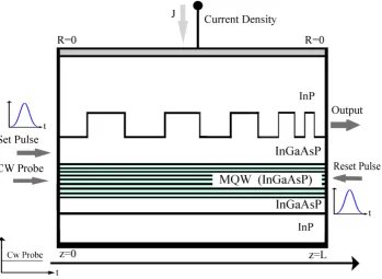
The paper is organized as follows. Section II explains the device structure and the parameters that used Figure 1: Schematic diagram of a MQW liner chirped DFB-SOA
192
in an all optical flip flop. Section III describes the
static dynamic responses of DFB-SOA all optical
flip flop switching based on XPM and the MQW
effects on switching ON and OFF time. Finally, Section IV summarizes the essential points of this investigation with the Conclusion.
Figure 2: modal gain versus photon energy for different carrier density in a MQW ragion
2. DFB-SOA STRUCTURE
In order to study the fundamental characteristics of
an all-optical flip-flop, we consider a longitudinally
multi quantum well linear chirped DFB-SOA
operating at 1550nm [12]. The device structure and
its parameters, used in our simulation, are shown in Figure 1, and Table I, respectively. In the active layer, we used single or multiple quantum wells with or without strained effects. To show the effects
of quantum well on the DFB-SOA all optical flip flops, we first used single quantum well with 75Ao
and calculate the modal gain. Then, we chose 14 well with compression strained MQW. All the other
needed active layer parameters are in [13].
The model structure is assumed to be a
traveling-wave type DFB-SOA with no facets reflections
merely supporting a single transverse mode. Furthermore, the current is considered to be uniformly injected into the entire area of the device, while the local carrier densities vary with position in the active region. Thus, the carrier density in each section can be derived from the corresponding rate
equations. As illustrated in Figure 1, a continuous wave (CW) probe light with constant power, as well as a control light set signal are injected into the active region, from the left. Meanwhile, a reset signal is injected from the right. When the set and rest pulses are injected separately, the injection
scheme is known as XPM based switching [3].
Table I. Geometrical and Physical parameters used in the device simulation.
Symbol Description Value Unit
L Active region length 300 μm
ГMQW Optical confinement factor 0.344 -ГQW Optical confinement factor 0.125 -αm Linewidth enhancement factor 2.5
-C Liner chirp coefficient 6
-n Modal refractive index 3.2353 -σ Mode cross section 10-12 m2
κL Coupling coefficient 2
-R1=R2 Facets Reflectivities 0
-Anrad Nonradiative recombination constant 1×10⁸ s−1
Brad Radiative recombination constant 2.5×10⁻¹⁷ m3/s
CAug Auger recombination constant 9.4×10-41 m6/s
LQW Quantum well length 75 Ao
Lw Multiple quantum well length 190 Ao
Lb Multiple quantum well barrier length 470 Ao ГL(MQW) Broadening factor of MQW 30 meV Г L(QW) Broadening factor of QW 10 meV
3. SIMULATION RESULT
Using the modified time dependent TMM and
FDTD method, we have numerically simulated the performance of a DFB-SOA as well as a MQW
liner chirped DFB-SOA. To confirm the validity
of the analysis, we have compared our simulation results for the conventional DFB-SOA with the
results of TMM method [3]. As a starting point
for the simulation, the carrier densities in each section are obtained by solving the carrier density rate equation. Finding N(z,t) allows us to calculate
the modal gain, Γg, within the strained single and
multiple quantum well layer in each section with
finite difference method.
193
We have assumed that the duration of the input pulseis much longer than the round-trip time in the cavity. Thus, the solutions to the forward and backward propagating wave equations can be obtained by using TMM and FDTD method. Splitting the length
L into M(=30) equal sections makes the computation
speed and accuracy appropriate.
Figure 3: Maximum modal gain versus carrier density for a different QW (x=0.68), compression
strained QW (x=0.37), MQW (x=0.468) and compression strained MQW (x=0.37).
3.1. Quasi Static Response
As was mentioned before, QW or MQW with or without strained effects are used in the active layer
in the DFB-SOA all optical flip flop. So, to show the
quantum well effects on the dynamic behavior of an
all optical flip, the modal gain of a MQW region is
plotted in Fig. 2 for different carrier density. To avoid
confusion, the detailed definitions of the important
basis functions, and strains due to external stress
and lattice mismatch aren’t wrote in this paper [15].
We also tabulate the important parameters used in our work in the Table I.
Thus MQW as well as strained MQW region have the higher differential gain than QW region, the
dependence of the maximum modal gain, Γg for TE polarization calculated from the Fig 2 for an InGaAsP/InP MQW versus the carrier density is shown in Fig.3. In the same figure, the maximum
modal gain for a strained MQW and a QW with and
without strained effects are shown for comparison, versus carrier density. As can be seen from these results, the slop as well as differential gain of compression strained MQW with fraction mole
x=0.37 is larger than the MQW and QW with and
without strained. These results have good agreement
with the results of [15] and [16]. It is well known that
the differential gain of tension strained MQW is less than the MQW and compression strained MQW, so
we ignore these kind of region in our work [15].
density is shown in Fig.3. In the same figure, the maximum ١
modal gain for a strained MQW and a QW with and without ٢
strained effects are shown for comparison, versus carrier ٣
density. As can be seen from these results, the slop as well as ٤
differential gain of compression strained MQW with fraction ٥
mole x=0.37 is larger than the MQW and QW with and ٦
without strained. These results have good agreement with the ٧
results of [15] and [16]. It is well known that the differential ٨
gain of tension strained MQW is less than the MQW and ٩
compression strained MQW, so we ignore these kind of ١٠
region in our work [15]. ١١
١٢
To obtain the static responses, we apply each input for ١٣
10.8ns which is much longer than the round trip in a 300μm ١٤
active region, satisfying the quasi static condition. In order to ١٥
characterize the device behavior, we need to calculate the ratio ١٦
of the output power to the small signal input power, known as ١٧
the optical transmittivity, as a function of the wavelength. To ١٨
trace out the transmittivity curve, a single CW light signal is ١٩
injected into QW or MQW liner chirped DFB-SOA from the ٢٠
left. Then, after 10.8ns, the output power is calculated as a ٢١
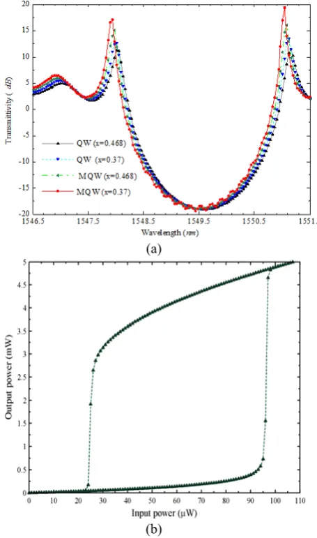
function of wavelength. Figure 4a demonstrates the ٢٢
transmittivity curves for various active layer regions, QW and ٢٣
MQW with and without strained, while grating coupling ٢٤
coefficient, κL and the chirp coefficient (C) are kept constant; ٢٥
e.g. κL=2 and C =6 that corresponding to chirped DFB-SOA. ٢٦
Figure 4b show the dependence of optical output power versus ٢٧
optical input power to show the bistability behavior of an ٢٨
DFB-SOA AOFF. An alternative method to latch the flip-flop ٢٩
operation is the switching action based on XPM. This is done ٣٠
as the set and reset signals are separately injected to DFB-٣١
SOA along with the holding beam (CW input light). A XPM ٣٢
based switching process is similar to that of SPM based, ٣٣
except that the holding beam power is adjusted in the center of ٣٤
the hysteresis loop and control signal (set or reset pulses) are ٣٥
injected to the device separately ٣٦
٣٧
To compare the effects of quantum well and strains on ٣٨
chirped DFB-SOA all optical flip flop in Figure 3, the current ٣٩
is adjust to 12.16mA. As shown in Figure 3, the chirped DFB-٤٠
SOA all optical flip flop with strained MQW layer in active ٤١
region give a larger transmittivity at Bragg resonance than the ٤٢
other type of active layer region. This is because the larger ٤٣
modal gain causes the larger amplification and therefore the ٤٤
Fig.2: modal gain versus photon energy for different carrier density in a MQW ragion
Fig. 3: Maximum modal gain versus carrier density for a different QW (x=0.68), compression strained QW (x=0.37), MQW (x=0.468) and compression strained MQW (x=0.37).
(a)
(b)
Fig. 4: a)Transmittivity versus wavelength for different active layer regionFigure 4: b) output power versus input power. a)Transmittivity versus wavelength for
different active layer region b) output power versus input power.
To obtain the static responses, we apply each input for 10.8ns which is much longer than the
round trip in a 300μm active region, satisfying the
194
quasi static condition. In order to characterize the device behavior, we need to calculate the ratio of the output power to the small signal input power, known as the optical transmittivity, as a function of the wavelength. To trace out the transmittivity curve, a single CW light signal is injected into QW or MQW liner chirped DFB-SOA from the left. Then, after 10.8ns, the output power is calculated as a function of wavelength. Figure 4a demonstrates the transmittivity curves for various active layer regions, QW and MQW with and without strained,
while grating coupling coefficient, κL and the chirp coefficient (C) are kept constant; e.g. κL=2 and C=6
that corresponding to chirped DFB-SOA. Figure 4b show the dependence of optical output power versus optical input power to show the bistability behavior of an DFB-SOA AOFF. An alternative method
to latch the flip-flop operation is the switching
action based on XPM. This is done as the set and reset signals are separately injected to DFB-SOA along with the holding beam (CW input light). A XPM based switching process is similar to that of SPM based, except that the holding beam power is adjusted in the center of the hysteresis loop and control signal (set or reset pulses) are injected to the device separately.
To compare the effects of quantum well and strains
on chirped DFB-SOA all optical flip flop in Figure 3, the current is adjust to 12.16mA. As shown in Figure 3, the chirped DFB-SOA all optical flip flop with strained MQW layer in active region
give a larger transmittivity at Bragg resonance than the other type of active layer region. This is because the larger modal gain causes the larger
amplification and therefore the larger transmittivity
is obtained. Also, the amounts of transmittivity in shorter wavelengths are less than transmittivity in the longer wavelengths because the DFB-SOA
experiences a non equal amplification for different
wavelengths. Here we don’t mention to the effects
of grating coupling coefficient and chirp coefficient because these are explained in [12].
The peak of transmittivity at the Bragg resonance
approaches infinity (in theory) when the bias
current increases. The SOA reaches the threshold condition at which it produces output light without any input (i.e. SOA operates as a laser). As shown in
the Figure3, little perturbation occurs with strained
MQW because the current of 12.16mA cause the chirped DFB-SOA operate below the threshold condition.
larger transmittivity is obtained. Also, the amounts of
١
transmittivity in shorter wavelengths are less than
٢
transmittivity in the longer wavelengths because the
DFB-٣
SOA experiences a non equal amplification for different
٤
wavelengths. Here we don’t mention to the effects of grating
٥
coupling coefficient and chirp coefficient because these are
٦
explained in [12].
٧
The peak of transmittivity at the Bragg resonance
٨
approaches infinity (in theory) when the bias current
٩
increases. The SOA reaches the threshold condition at which
١٠
it produces output light without any input (i.e. SOA operates
١١
as a laser). As shown in the Figure3, little perturbation occurs
١٢
with strained MQW because the current of 12.16mA cause the
١٣
chirped DFB-SOA operate below the threshold condition
١٤ ١٥
B. Dynamic responses
١٦
To obtain the dynamic responses, first we give the
١٧
bistability curves and the mention to the dynamic responses.
١٨
To trace out the bistability curves, we first increase the input
١٩
power and calculate the output power. Then, we decrease the
٢٠
input power and recalculate the output power. To do this, we
٢١
apply each input for 10.8ns which is much longer than the
٢٢
active region round-trip of ~3ps. This choice ascertains the
٢٣
quasi static condition.
٢٤
The two output states of an optical flip–flop are based on
٢٥
optical bi-stability in a DFB-SOA which are simply where the
٢٦
input power (holding beam) intersects the two branches of the
٢٧
hysteresis curve. The output power can be switched between
٢٨
ON and OFF states by injecting the set and reset pulse signals,
٢٩
respectively. This behavior demonstrates that the switching
٣٠
action is based on XPM. The set pulse signal, like the holding
٣١
beam, drops within the SOA gain spectrum and hence
٣٢
stimulates recombination of electron-hole pairs.
٣٣
Recombination makes the gain to saturate and the refractive
٣٤
index to increase.
٣٥ ٣٦
Thus, the set signal modulates the wavenumber and phase
٣٧
of the holding beam along the structure. In our application, the
٣٨
increase in refractive index pushes the Bragg resonances to
٣٩
longer wavelengths. Upward switching occurs when the
٤٠
Bragg resonance has been shifted sufficiently to initiate the
٤١
positive feedback loop. In terms of the hysteresis curve, using
٤٢
XPM to shift the Bragg resonance toward the holding-beam
٤٣
wavelength corresponds to the case of pushing the switching
٤٤
threshold to a lower power. The sign of XPM for the reset
٤٥
signals is opposite to that of the set signals, whereas the reset
٤٦
signal wavelength drops out of the SOA gain spectrum and is
٤٧
absorbed in the active region of SOA. Here, it is supposed that
٤٨
the control signals (set and reset signals) travel in the
DFB-٤٩
SOA without any interaction with the grating. To investigate
٥٠
the flip flop operation in all figures, the set and reset signal
٥١
wavelengths are tuned at λs=1555nm and λr=1310nm,
٥٢
respectively, where the holding beam wavelength is adjusted
٥٣
0.3nm larger than the Bragg wavelengths according to the
٥٤
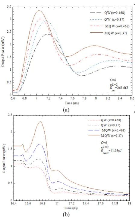
Figure 4. The dynamic behavior of MQW chirp DFB-SOA all
٥٥
optical flip flop based on XPM is illustrated in Figure 5. The
٥٦
holding power is adjusted in the middle of hysteresis loop.
٥٧
The control signals with Gaussian shape are separately
٥٨
injected into the device from the left and right where the
٥٩
device operates as a flip flop. The reason is that, the set signal
٦٠
from the left experience a large amplification due to the high
٦١
material gain, therefore large carrier density depletion is occur
٦٢
in the output end of the device. So, to choose the appropriate
٦٣
injection direction of reset signals, injection from the right
٦٤
increase the carrier density and as a result the speed of flip
٦٥
flop rises. The energies of set and reset pulse signals with the
٦٦
same FWHM of 100ps are Eset=265.6fJ and Ereset=11.63pJ,
٦٧
respectively. As is shown in figures 5a, the switch ON time
٦٨
decreases when the strain MQW active layers is chose. This is
٦٩
because the large differential gain decreases the effective
٧٠
carrier lifetime. Therefore carrier density experiences the
٧١
faster recovery time and as a result the switching ON time
٧٢
improves. We note that the switching OFF time increases
٧٣
when the differential gain increase and limit the switching
٧٤
speed as is shown in Figure 5b.
٧٥
(a)
(b)
Fig. 5: (a) Rise time and (b) fall time versus time with different active layer region. Figure 5: (a) Rise time and (b) fall time versus
time with different active layer region.
3.2. Dynamic Responses
To obtain the dynamic responses, first we give the
bistability curves and the mention to the dynamic responses. To trace out the bistability curves, we
first increase the input power and calculate the
output power. Then, we decrease the input power and recalculate the output power. To do this, we apply each input for 10.8ns which is much longer
than the active region round-trip of ~3ps. This
choice ascertains the quasi static condition.
The two output states of an optical flip–flop
195
are based on optical bi-stability in aDFB-SOA which are simply where the input power (holding beam) intersects the two branches of the hysteresis curve. The output power can be switched between ON and OFF states by injecting the set and reset pulse signals, respectively. This behavior demonstrates that the switching action is based on XPM. The set pulse signal, like the holding beam, drops within the SOA gain spectrum and hence stimulates recombination of electron-hole pairs. Recombination makes the gain to saturate and the refractive index to increase.
Thus, the set signal modulates the wavenumber and phase of the holding beam along the structure. In our application, the increase in refractive index pushes the Bragg resonances to longer wavelengths.
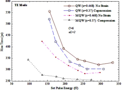
Figure 6: Rise time versus set pulse energy for different active layer region.
Upward switching occurs when the Bragg resonance
has been shifted sufficiently to initiate the positive
feedback loop. In terms of the hysteresis curve, using XPM to shift the Bragg resonance toward the holding-beam wavelength corresponds to the case of pushing the switching threshold to a lower power. The sign of XPM for the reset signals is opposite to that of the set signals, whereas the reset signal wavelength drops out of the SOA gain spectrum and is absorbed in the active region of SOA.
Here, it is supposed that the control signals (set and reset signals) travel in the DFB-SOA without any interaction with the grating. To investigate the
flip flop operation in all figures, the set and reset signal wavelengths are tuned at λs=1555nm and λr=1310nm, respectively, where the holding beam wavelength is adjusted 0.3nm larger than the Bragg
wavelengths according to the Figure 4. The dynamic behavior of MQW chirp DFB-SOA all optical
flip flop based on XPM is illustrated in Figure 5.
The holding power is adjusted in the middle of hysteresis loop. The control signals with Gaussian shape are separately injected into the device from the left and right where the device operates as
a flip flop. The reason is that, the set signal from the left experience a large amplification due to the
high material gain, therefore large carrier density depletion is occur in the output end of the device. So, to choose the appropriate injection direction of reset signals, injection from the right increase the
carrier density and as a result the speed of flip flop
rises. The energies of set and reset pulse signals
with the same FWHM of 100ps are Eset=265.6fJ and Ereset=11.63pJ, respectively.
As is shown in figures 5a, the switch ON time
decreases when the strain MQW active layers is chose. This is because the large differential gain decreases the effective carrier lifetime. Therefore carrier density experiences the faster recovery time and as a result the switching ON time improves. We note that the switching OFF time increases when the differential gain increase and limit the switching
speed as is shown in Figure 5b.
4. CONCLUSION
In this paper, we have investigated the dynamic responses of a QW and MQW chirped DFB-SOA
all optical flip flop based on XPM mechanism. In
addition, the effects of strains on the rise and fall times are investigated. We solved the coupled-mode and carrier rate equations in the time domain under low-intensity regime. We found that the energy of set and reset pulses can be reducing by strained
MQW active region. The rise time decrease to 250ps with energy of set pulse 256.6fJ. Unfortunately, the
fall time can’t improve with such an active region. Hence, using strained MQW active region leads to good reduction in switching ON time but can’t decrease the switching OFF time.
196
REFERENCES
1. S. J. B. Yoo, “Optical packet and burst switching
technologies for the future photonic internet,” IEEE
J. Lightwave Technol. 24, 4468-4492, (2006). 2. M. Takenaka, K. Takeda and Y. Nakano, “All-optical
packet switching and label buffering by MMI-BLD
optical flip-flop,” IEICE Elec. Express. 3, 368-372,
(2006).
3. D. Maywar, G. P. Agrawal and Y. Nakano, “Robust
optical control of an optical-amplifier-based flip-flop,” Opt. Exp. 6, 75-80, (2000).
4. W. D’Oosterlinck, F. Ohman, J. Buron, S. Sales and
A. P´erez Pardo, “All-Optical flip-flop operation
using a SOA and DFB laser diode optical feedback
combination,” Opt. Express 15, 6190-6199, (2007).
5. W. D’Oosterlinck, J. Buron, F.Öhman, G. Morthier
and R. Baets, “Alloptical flip-flop based on an SOA/ DFB-laser diode optical feedback scheme,” IEEE
Photon. Technol. Lett. 19, 489-491, (2007).
6. W. D’Oosterlinck, G. Morthier, R.Baets and
T.Erneux, “Optical bistability in a traveling-wave
SOA Connected to a DFB Laser Diode: Theory and
Experiment,” IEEE J. Quantum Electron., 42,
739-746, (2006).
7. K. Huybrechts , W. D’Oosterlinck, G. Morthier and
R. Baets, “Proposal for an All-optical flip-flop using a single distributed feedback laser diode,” IEEE
Photon. Technol. Lett. 20, 18-20(2008).
8. Y. Kim, J. H. Kim, S. Lee, D .H. Woo, S. H. Kim and T. H. Yoon, “Broad-Band All-Optical Flip–Flop
Based on Optical Bistability in an Integrated SOA/ DFB-SOA,” IEEE Photon. Technol. Lett. 16.
398-400, (2004).
9. A. Aleshams, M. K. Moravvej-Farshi and M. H. Sheikhi, “Tapered grating effects on static properties of a bistable QWS-DFB semiconductor
laser amplifier,” Solid-State Electron. 52, 156-163,
(2008).
10. M. Aleshams, M. K. Moravvej-Farshi, and M. H. Sheikhi, “Switching Behavior of Bistable DFB
Semiconductor Laser Amplifiers”, Fiber and
Integrated Optics, Accepted for Publication (2008). 11. L. Zhang, I. Kang, A. Bhardwaj, N. Sauer, S. Cabot,
J. Jaques and et al., “Reduced Recovery Time
Semiconductor Optical Amplifier Using p- Type-Doped Multiple Quantum Wells,” IEEE Photon. Technol. Lett. 18, 2323-2325, (2006).
12. M. Jabbari, M. K. Moravvej-Farshi, R. Ghayour and A. Zarifkar, “XPM Response of a Chirped DFB-SOA All-Optical Flip-Flop Injected with an Assist
Light at Transparency,” IEEE J. Lightwave Technol.,
Accepted for Publication (2008).
13. S.L.Chuang, “Efficient-Structure Calclution of
Strained Quantum Well”,The American Physical
Society, Vol.43, No. 12, pp. 9649-9661, 1991.
14. K.Kikuchi, M.Kakui, C .E. Zah and T. P. Lee,
“Diffrential gain and linewidth enhancement factor
of 1550nm MQW active layer with without Biaxialy compression strain”, IEEE Photon. Technol. Lett., vol. 3, No.4, pp. 314-318, 1991.
15. D. Ahn and S. L. Chuang, “ Optical gain in a strained
layer quantum well laser”, IEEE J. Quantum
electron., Vol. 24, No. 12, pp. 2400-2406, Dec. 1988.