ALL-OPTICAL BINARY COUNTER BY
USING T FLIP-FLOP: AN
IMPLEMENTATION
SAMIR SAHU
Department of Physics and Technophysics Vidyasagar University
Midnapur – 721102 West Bengal, India [email protected]
RADHA RAMAN PAL
Department of Physics and Technophysics Vidyasagar University
Midnapur – 721102 West Bengal, India [email protected]
SHANTANU DHAR
Department of Physics Jhargram Raj College Jhargram – 721507
West Bengal, India [email protected]
ABSTRACT: All-optical T (Toggle) flip-flop with preset (PR) and clear (CLR) are basic building modules for the development of ultra-high speed all optical binary counter. In this paper, a non-linear material based all-optical switching mechanism is utilized here to realize the all-all-optical T flip-flop with PR and CLR. A composite slab of linear medium (LM) and non-linear medium (NLM) is used to design the all-optical switch that exploit the attractive features of NLM. These all-optical T flip-flops can find application in the development of several complex all-optical circuits of enhanced performances. Here we demonstrate an all-optical binary 3-bit ripple counter which is nothing but the successive application of the flip flop. This circuit can elevate to a higher bit different counters. As this all optical circuits are purely all-optical in nature, these are very simple as well as very fast. Also the schemes have capacity of cascading.
Keywords: nonlinear material; all-optical logic gate; all-optical flip flop.
1. Introduction
With the increasing data traffic day-by-day, there is a requirement to restrict research problems in a particular region to achieve the reliable, faithful and high speed performances in communication [Mukhopadhyay et al.
(2008);] has established its validity as one of many promising techniques [Pei-Li et al. (2008); Dutta and Mukhopadhyay, (2010)]. This is used to develop various combinational logic circuits [Wang et al. (2009)] as well as sequential logic circuits [Wang et al. (2010)] by many scientists and technologists. For example, all optical flip-flops are key devices for realizing many functionalities in optical networks, optical computing, especially as all-optical memories for the temporary storage of data.
Several optical flip-flops using different techniques have already been proposed [Dhar and Sahu, (2008); Wang et al. (2010)]. An all-optical S-R, S-R with clock, D, J-K and J-K master-slave type flip-flops using non-linear material [Dhar and Sahu, (2008); Sahu and Dhar, (2009)] was also reported.Now, in our present paper we proposed a scheme for all optical implementation of synchronous T flip-flop using non-linear material as all optical switches. As this all optical flip-flop is purely all-optical in nature, it is very simple as well as very fast. The advantageous side of our scheme is that there are two outputs which are complemented to each other. Also the scheme has capacity of cascading. The output of the T flip-flop and its complement are obtained simultaneously in our scheme. The initial state of the flip flop can also be assigned by the inputs PR and CLR.
Binary counters are often required to count events. Existing electronic counter are slow. To gear up the performance speed it is essential to replace existing digital counter by all optical counter. Various all-optical counters have been reported [Wang et al. (2009); Wang et al. (2010)]. At the end of our present paper we implement an all-optical binary 3-bit counter by the successive use of the T flip flop with PR and CLR. It is a ripple (asynchronous) counter. The outputs of the counter can be erased out by the clear input. This circuit can raise to a higher bit several types of counters. These circuits are key elements for the implementation of a high-speed, all-optical data processing device, which has the potential to outperform its electronic equivalent and constitute a possible new product for our dream goal, optical computer.
2. All-Optical Switching Behavior of Nonlinear Material
The phenomenon photorefractivity [Arivouli, (2001); Sahu and Dhar, (2009)] of some nonlinear optical material is used in nonlinear all-optical intensity switching mechanism. The photorefractive effect, where the refractive index changes induced by a light field when the crystal is subjected to intense laser radiation, defocusing and scattering of the light, is observed, as a result of an inhomogeneous change in the refractive index. It is also found that these changes still prevail even after the light is switched off, but it could be erased by strong, uniform illumination [Arivouli, (2001)].The refractive index of some nonlinear materials (NLM) such as carbon disulfide, pure silica, potassium dihydrophosphate (KDP) crystal etc. varies linearly with the intensity of the light incident on it. The refractive index (n) of such isotropic dielectric non-crystalline media can be put into an equation as Eq. (1). Here n0 is the linear term, n1 is the nonlinear correction term and I is the intensity of the
incident light beam on the material.
n = n0 + n1 I (1)
We can implement the switching mechanism with such nonlinear material by taking an interface between two media of which one is a linear material (LM), whose refractive index n0 is independent of the intensity of
light and the other is aforesaid NLM. A laser beam, highly intense polarized light, preferably pulse laser of
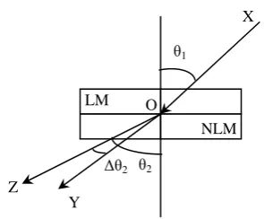
Fig. 1. Intensity switching of optical nonlinear material
NLM
LM O
Z
Y
X
θ1
θ2
intensity I1, is allowed to incident on the interface from linear to nonlinear part in a particular direction XO
(incidence angle θ1) as depicted in Fig. 1. The refracted beam from the NLM follows the path OZ (angle of
refraction θ2). But when another higher intense laser beam of intensity I2 (I2> I1) is made to incident along XO,
after refraction from the NLM the light passes through OY direction. The deviation of refractive angle for different incident light intensity I1 and I2 is <ZOY = Δθ2. Thus the combination of LM and NLM may act nicely
as a directional all-optical switch. This is the unit block of our proposed T flip-flop and binary counter circuit. In the expression of refractive index in Eq. (1), n0 is linear term and n1 is the nonlinear correction term. For
carbon disulfide [Samanta and Mukhopadhyay, (2007); Sahu and Dhar, (2009)] (CS2) n0 = 1.63, n1 = 514×10-20
m2/W. and for fused silicon dioxide [Samanta and Mukhopadhyay, (2007); Sahu and Dhar, (2009)] (SiO2) n0 =
1.458, n1 = 2.7×10⁻²⁰ m2/W. If we use CS2 and SiO2 as nonlinear materials and the pulse laser of intensity I =
2×10¹⁸ W/m2 as a source, we can estimate the deviations of light in two cases as given in Table 1.
3. All-Optical NOT Gate And AND Gate
The logic gates [Choudhury and Mukhopadhyay, (2003); Dhar and Sahu, (2008); Sahu et al. (2011)] are implemented in optics using NLM by taking the presence of light signal as 1 and the absence of it as 0. The implementation of such logic gates can be done by using some femtosecond laser pulses and 1-mm-thick potassium dihydrophosphate (KH2PO4 (KDP) crystal at the pick intensity of 0.6 TW/cm2 and duration of 60 fs
[Mironov et al. (2009); Sahu and Dhar, (2009)].
3.1 All optical NOT gate
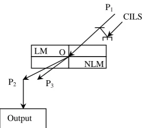
To implement an all optical NOT gate using non-linear material a constant intensity pulse laser source (CILS) is used as shown in Fig. (2). It is also called probe beam. Here P1 is taken as input beam. A detector is placed at P2
will detect the output beam after refraction. If P1 is absent, the light will follow a path OP2 and will be detected
Material Angle of incidence (θ1)
Incident light intensity
n (= n0 + n1 I)
Angle of refraction (θ2)
Deviation (Δθ2 = θ′2 - θ′′2)
carbon disulfide
(CS2)
45 deg I=2×10¹⁸ W/m2 11.91 3.404 deg = θ′2
1.578 deg
45 deg 2I 22.19 1.827 deg= θ′′2
silicon di-oxide
(SiO2)
45 deg I=2×10¹⁸ W/m2 1.512 27.883 deg= θ′2
1.041 deg
45 deg 2I 1.566 27.842 deg= θ′′2
NLM
LM O
P2 P3
P1
CILS
Output
Fig. 2. All-optical NOT gate
by the detector due to presence of CILS. But if P1 is present, after refraction, the light will follow a path other
than OP2, may be OP3, and the detector will not detect any light signal. Thus the system acts as optical NOT
gate.
3.2 All Optical AND gate
The all-optical AND gate using two inputs and three inputs are shown in Fig. 3. The two inputs all-optical AND gate using NLM is shown in Fig. 3(a). Here R1 and R2 are two input channels. A detector placed at R4 gives the
output. Now when both the channels carry light signal, the light beam after refraction will detected by the detector at R4, unless not.
The three inputs all-optical AND gate using NLM is shown in Fig. 3(b). Here T1, T2 and T3 are three input
channels. A detector placed at T6 gives the output. Now when all the channels carry light signal, the light beam
after refraction will detected by the detector at T6, unless not.
4. Conventional Electronic Flip-Flops
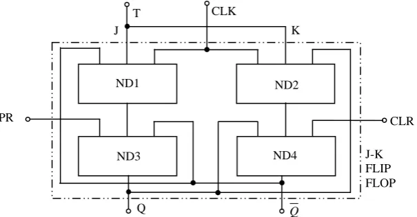
A flip-flop is a device with two stable states. It remains in one of these states until triggered into other. Fig. 4 shows the block diagram of conventional electronic T flip-flop with PR and CLR [Morris Mano, (2000); Jain, (2007)]. The T flip-flop is obtained from a J-K flip-flop with PR and CLR [Sahu and Dhar, (2009)] if both inputs are coupled together as in Fig. 4. The ND1...ND4 are electronically addressed NAND gates. The modified truth tables T flip-flop with PR and CLR are given bellow in Table 2.
(a)
NLM
LM O
R3 R4
R1
R2
Output
NLM
LM O
Output
T1
T3
T2
T6
T5
T4
(b)
Fig. 3. All-optical AND gate using NLM. (a) two-input AND gate. (b) three-input AND gate
Fig. 4. Electronically addressed T flip-flop with preset and clear
Q Q
ND1 ND2
ND3 ND4
J K
CLK T
J-K FLIP FLOP
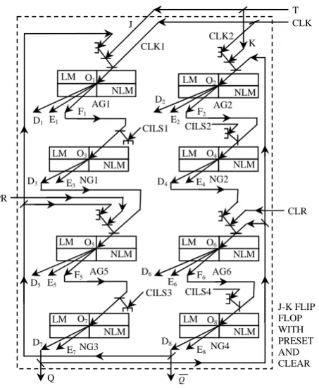
5. All Optical T Flip-Flop With Preset (PR) and Clear (CLR)
Now we talk about the fundamental design of the all-optical circuit of the T flip-flop with preset (PR) and clear (CLR) as shown in Fig. 5. Here T is the input and Q and Q are the final output states of the T Flip-Flop. There are four all-optical AND gates (AG1, AG2, AG5 and AG6) and four all-optical NOT gates (NG1, NG2, NG3 and NG4) in our proposed circuit. All the four AND gates are three-inputs AND gates. The input T is the constant intensity light source, preferably pulse laser. The T is connected to one of the three inputs of both the AG1 (J) and AG2 (K) respectively. CLK, clock pulse in the form of pulse laser of similar intensity as T, is
divided to CLK1 and CLK2 which are used as second inputs of AG1 and AG2 respectively. Feed backs from Q
and Q are the third inputs of AG1 and AG2 respectively. F1 and F2, the respective outputs of AG1 and AG2, are
used as the input of two corresponding NOT gates, NG1 and NG2. Two constant intensity light sources CILS1
Inputs Outputs State
CLK1 = CLK2
PR CLR Qn T Qn+1 Qn+1
0 1 1 d d Qn Qn Previous
1 1 1 0 0
0 0 Qn 1 Qn Previous
1 1 1 0 0 1 0
1 1 1 1 1
1 1 Q
n
0
Qn Toggle
1 1 1 1 1 0 1
0 1 0 d d 0 1 Clear
0 0 1 d d 1 0 Preset
Fig. 5. All-Optical T Flip-Flop with Preset (PR) and Clear (CLR) Using NLM as Switch
CLK
CLR PR
J-K FLIP FLOP WITH PRESET AND CLEAR
Q
NLM
LM O7
NLM
LM O8
CILS3
Q
NG3 NG4
D7
E7 E8
D8
CILS4 NLM
LM O3
NLM
LM O4
CILS1
NG1 D4 NG2
D3 E3 E4
CILS2
D5 E5
NLM
LM O5
F5 AG5 D6
E6
NLM
LM O6
F6 AG6
D1
NLM
LM O1
F1
AG1 J
D2
NLM
LM O2
F2
AG2
T
CLK1
CLK2 K
E1 E2
Table 2. Truth table of Clocked T flip-flop with Preset (PR) and Clear (CLR)
and CILS2 preferably pulse laser sources of similar intensity level are fed in the input channels of both the NOT gates NG1 and NG2 respectively as probe beams. The output beams from NG1 (D3) and NG2 (D4) are now used
as one of the inputs of AG5 and AG6 respectively. Q and Q the final output beams are fed to AG5 and AG6 respectively just like AG1 and AG2. The preset (PR) and clear (CLR) inputs are connected to AG5 and AG6 respectively as third input of each. F5 and F6 are the outputs of AG5 and AG6 respectively. Now F5 beam is
allowed to incident as the input beam of NG3. A probe beam CILS3 in the form of pulse laser is used for the proper action of NG3. Similarly, F6 beam is allowed to incident as the input beam along with a probe beam
(CILS4) of NOT gate NG4. The output D7 from NG3 is taken to be the final Q and output D8 from NG4 is taken
to be the finalQ of the all-optical T flip-flop.
Let us realize the operation of the clocked T flip-flop with preset (PR) and clear (CLR). First we consider PR = CLR = 1 i. e. both the inputs are at high state.
Now when the clock pulse beams are inactive i.e. CLK1 = CLK2 = 0, both the outputs F1 and F2 of AG1
and AG2 respectively, give 0 whatever may be the other inputs T of the flip-flop. As F1 = F2 = 0 the light will
be present at D3 and D4 position due to the probe beams CILS1 and CILS2 respectively. This light is fed in the
channel of the inputs of the AND gates AG5 and AG6. Here two possibilities may arise. Possibility 1; ifQ n = 0
and Qn = 1, then F5 = 0 and F6 = 1 consequently D7 = 1 and D6 = 0, i.e. the Qn+1th state preserve the Qnth state
and Qn+1th state also preserve the Qnth state. Possibility 2; if Qn = 1 and Qn = 0, then F5 gives 1 and F6 gives 0
consequently D7 gives 0 and D8 gives 1, again the Qn+1thstate and Qn+1th state follow the Qnth state and Qnth
state respectively.
When CLK1 = CLK2 = 1 (i.e. active part of the clock pulse beam), two circumstances may occur. They are as follow:
Let T is inactive (i.e. J = K = 0). Then there will be no light at both the output terminals F1 (from AG1) and F2
(from AG2) irrespective of the other two inputs of AG1 and AG2. The outputs Q and Q are latched to their previous state very similar to the aforesaid condition (CLK1 = CLK2 = 0; J, K whatever may be).
Now, we consider the other possible input T = 1. That means J and K both become active. Here two cases may arise, case 1; if Qn = 1 and Qn = 0, then F1 = 1 and F2 = 0 therefore, D3 = 0 and D4 = 1. As the output of
AND gate gives 0 when any one input is inactive irrespective of the other inputs, there is no light signal present at F5 (i.e. F5 = 0). As a result the output of NG3 will be 1, i.e. D7 = Qn+1 = 1. Now, AG6 has two inputs, one is Q
and the other is D4 and both the input terminals have light signal. Since, Q = D4 = 1, light will follow the path
O6F6 (i.e. F6 = 1). Then D8 or Qn+1 will become 0 as both the input beams F6 and probe beam CILS4 of NG4 are
present. Case 2; if Qn = 0 and Qn = 1, F1 = 0 and F2 = 1, as a result D3 gives 1 and D4 gives 0. Since, AG6 is an
AND gate and D4 = 0 is one input of it, the light will appear at E6 terminal. So, F6 = 0 and hence D8 = 1 i.e. Qn +
1 = 1. Now, AG5 has inputs D3 = 1 and Q = 1. F5 = 1 and outcome of this is D7 = 0. That means Qn+1 state is
now become 0. Thus here the circuit always changes state and complement to previous output i.e. if Qn = 1 it
switches to Qn+1 = 0 and vice versa. The truth table is shown in Table 2.
The outputs of the T flip-flop are the function of data inputs T if the clock pulses are present (CLK1 = CLK2 = 1) and preset and clear inputs carry light (PR = CLR = 1). However the output states are assumed arbitrary before the application of light pulses. The initial state of the flip-flop can be assigned by changing the state of the two terminals preset (PR) and clear (CLR).
Now we want to discuss the operation of preset and clear the output of this flip-flop. We know when clock is absent (CLK1 = CLK2 = 0), D3 = D4 = 1. If we take PR = 1 and CLR = 0, F6 = 0 whatever may be the other
two inputs of AG6. As a result D8 = Q = 1. Now the three inputs of AG5 are active (i.e. D3 = Q = PR = 1) and
the output F5 becomes 1 consequently D7 = Q = 0.
If we consider PR = 0 and CLR = 1, F5 = 0 irrespective of the other inputs of AG5. Due to the probe beam
CILS3 we get light at D7 terminal i.e. D7 = Q = 1. Now all the three inputs of AG6 become 1 (D4 = Q = CLR =
1). F6, the output channel of AG6, will carry light. As the NOT gate NG4 has input F6 = 1, along with probe
beam CILS4, D8 = Q = 0.
So we can conclude that in T flip-flop we need high CLR (=1) for preset the flip-flop (i.e. Q = 1 and Q = 0) and high PR (=1) for clear the flip-flop (i.e. Q = 0 and Q = 1). When PR = CLR = 1 i.e. both are high the outputs of the T flip-flop with preset (PR) and clear (CLR) will remain same as T flip-flop without preset (PR) and clear (CLR), shown at the first five rows in Table 2.
design the all optical NOT gate has an advantage. When ever the output of a NOT gate is assumed to be at ‘1’ state, the source of that ‘1’ state is a constant intensity pulse laser source (CILS) used as probe beam. So in each feedback arrangement described in our scheme similar intense light beam is fed back. In this way the reduction of intensity by using beam splitter will not affect the non-linear response of the device. The light sources are so chosen that each input beam intensity is in the rang of intensity which is detected as ‘1’ by the detector.
In T flip-flop due to feed back connection a problem may arise. If the active states of the clock pulses CLK1 and CLK2 are so large that they remain 1 (while T = 1) after the output has been complemented, the action of complementation of output will repeat. Then the problem is same as electronic circuits and it is called race-around [Sahu and Dhar, (2009)] problem. Therefore the duration of clock pulse should be chosen critically.
6. All Optical Binary Counter
The all optical binary counters are consisted of all optical T flip-flop. A 3-bit all optical binary counter is depicted in Fig. 6, which is composed by three all optical clocked T flip-flop (T flip flop 0, 1 and 2) with preset (PR) and clear (CLR) discussed earlier. The flip-flops are cascaded one by one to form the ripple counter. All the PR inputs are connected together to form the preset (PR) of the counter. To get the clear (CLR) input of the counter we coupled together the three CLR terminals of three T flip flops. Q0, the output of the first flip flop is
connected to the CLK of the second flip flop and the output Q1 (from T Flip Flop 1) is inputted to clock of T
Flip Flop 2. The complemented outputs Q are left open. One can get complement of counted OP from
Q2Q1Q0. The optical clock pulses (OP) which we want to count are connected to the CLK of the first flip flop.
The outputs are taken from the terminals Q0 (LSB), Q1 and Q2 (MSB). 3-bit binary counter can count from
binary 000 (=0) to 111 (=7). Q0Q1Q2 is the 3-bit output of this counter.
Now we want to realize the operation of the all optical 3-bit binary counter.
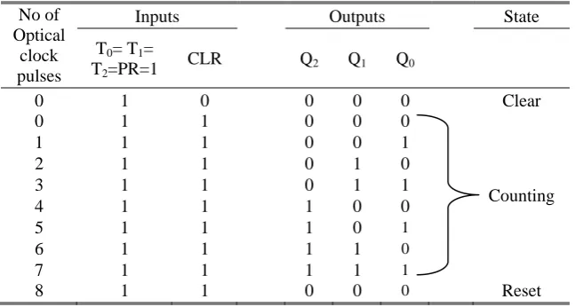
To performing the counting T0 = T1 = T2 = 1 and PR = CLR = 1 i. e. all the other inputs than clock are at
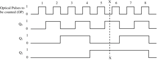
logical ‘1’. That means they carry light signal. The T flip flops, we proposed, are negative edge triggered type flip flops. The optical pulses and the output optical wave forms are illustrated in Fig. 7.
The output Q0 reverses its state at the negative edge of each optical pulse (OP) because T0 = 0. As Q0 acts as
CLK for T Flip Flop1 and T1 = 1, Q1 alters at negative edge of each Q0. Similarly Q2 is inverted at the negative
edge of Q1. At any instant, the binary number Q0Q1Q2 is the number of optical pulses counted till that time. At X
the count is 101 = 5. The output Q0Q1Q2 will be 000 after counting eight optical pulses. The output Q0Q1Q2 can
be clear by turn off light signal momentarily from CLR input. The truth table for 3-bit ripple counter is shown in Table 3. We can promote the 3-bit counter to n-bit binary counter with n flip flop having 2n possible states. A counter with a chain of n flip flops can count up to 2n -1 optical pulse.
No of Optical
clock pulses
Inputs Outputs State
T0= T1=
T2=PR=1
CLR Q2 Q1 Q0
0 1 0 0 0 0 Clear
0 1 1 0 0 0
Counting
1 1 1 0 0 1
2 1 1 0 1 0
3 1 1 0 1 1
4 1 1 1 0 0
5 1 1 1 0 1
6 1 1 1 1 0
7 1 1 1 1 1
8 1 1 0 0 0 Reset
Fig. 6. All Optical 3-bit Binary Counter Using T Flip Flops
Q2
NLM LM O7
NLM LM O8 CILS3
Q2
NG3 NG4
D7
E7 E8
D8 CILS4 NLM
LM O3
NLM LM O4 CILS1
NG1 D4 NG2
D3 E3 E4
CILS2
PR
D5 E5
NLM LM O5
F5 AG3 D6 E6
NLM LM O6
F6 AG4 D1
NLM LM O1
F1 AG1 J2
D2
NLM LM O2
F2 AG2 CLK1
CLK2 K2
E1 E2
CLK T2 CLR Q1 Q1 NLM LM O7
NLM LM O8 CILS3
Q1
NG3 NG4
D7
E7 E8
D8 CILS4 NLM LM O3 NLM LM O4 CILS1
NG1 D4 NG2
D3 E3 E4
CILS2
D5 E5
NLM LM O5
F5 AG3 D6 E6
NLM LM O6
F6 AG4 D1
NLM LM O1
F1 AG1 J1
D2
NLM LM O2
F2 AG2 CLK1
CLK2 K1
E1 E2
CLK T1 CLR Q0 (LSB) Q0 NLM LM O7
NLM LM O8 CILS3
Q0
NG3 NG4
D7
E7 E8
D8 CILS4 NLM LM O3 NLM LM O4 CILS1
NG1 D4 NG2
D3 E3 E4
CILS2
D5 E5
NLM LM O5
F5 AG3 D6 E6
NLM LM O6
F6 AG4 D1
NLM LM O1
F1 AG1 J0
D2
NLM LM O2
F2 AG2 CLK1
CLK2 K0
E1 E2
CLK T0
CLR
Q2 (MSB)
T Flip Flop 2 T Flip Flop 1 T Flip Flop 0
Preset (PR) Outputs
PR PR
Clear (CLR)
5. Conclusion
The proposed technique of all optical implementation of T flip-flop and binary counter is very fast (above THz) [Pei-Li et al. (2008); Mironov et al. (2009); Sahu and Dhar, (2009)] as it is fully all-optical. The light signals which are severally used and the feedback light signals from the outputs are made by mirrors and beam splitters to make the circuits simple. Another important feature is that all-optical temporary data storage memories may be developed by cascading the flip-flops. Other different types of Counter can be implemented from this ripple counter. Proper findings of non-linear material may be a significant issue here. Essentially inputs and constant intensity light source should be chosen properly to function the system accurately. The clock pulse signal should also be selected suitably.
Acknowledgment
The authors want to acknowledge Professor Sourangshu Mukhopadhyay of the University of Burdwan for his valuable suggestions.
References
[1] Arivouli, D. (2001): Fundamentals of optical nonlinear materials, Pramana, 57(5,6), pp. 871-883.
[2] Chen, C. H.; Matsuo, S.; Nozaki, K.; Shinya, A.; Sato, T.; Kawaguchi, Y.; Sumikura, H.; Notomi, M. (2011): All-optical memory
based on injection-locking bistability in photonic crystal lasers, Opt Express. 19(4) pp. 3387-3395.
[3] Choudhury K. R.; Mukhopadhyay, S. (2003) A new method of binary addition scheme with massive use of non-linear material based
system, Chin. Opt. Lett. 1(4),pp. 132-135.
[4] Dhar, S.; Sahu, S. (2008): All-optical implementation of S-R, clocked S-R and D flip-flops using nonlinear material, Optical
Engineering, 47( 6), pp. 065401-6.
[5] Dutta S.; Mukhopadhyay, S. (2010): An all optical approach of frequency encoded NOT based Latch using semiconductor optical
amplifier, J. of optics. 39(1), pp. 35–41.
[6] Jain, R. P. (2007) Modern Digital Electronic, 3rd edn.Tata MaGraw-Hill India, New Delhi.
[7] Mironov. S.; Lozhkarev, V.; Ginzburg, V. Khazanov, E. (2009): High-efficiency second-hermonic generation of superintense
ultrashort laser pulses, Applied Optics, 48, pp. 2051.
[8] Morris Mano, M. (2000) Digital Logic and Computer Design, 1st edn. Prentice-Hall of India Private Limited,New Delhi.
[9] Mukhopadhyay, S.; Datta, K. A.; Basuray, A. (1988): Optical computating: Researches in this decade, Optics, 17(4), pp. 94-100.
[10] Pei-Li, L.; De-Xiu, H.; Xin-Liang, Z.; Yang, W. (2008): Single-SOA-Based Ultrahigh-Speed All-Optical Half Subtracter with PolSK
Modulated Signals, Chin. Phys. Letters, 25(5), pp. 1705-1709.
[11] Sahu, S.; Dhar, S. (2009): Implementation of clocked J-K and J-K Master Slave flip-flops with nonlinear material in All-optical
Domain, Optical Engineering, 48( 7), pp. 075401-7.
[12] Sahu, S.; Pal, R. R.; Dhar, S. (2011): A Novel Method of Implementing Nonlinear Material Based All-Optical Binary Half Subtractor
and Full Subtractor System, J. of Electron Devices, 10, pp. 493-498.
[13] Samanta, D.; Mukhopadhyay, S. (2007): A method of maintaining the intensity level of a polarization encoded light signal, J. of
Physical Science,11,pp. 87-92.
[14] Wang, J.; Meloni, G.; Berrettini, G.; Potì, L.; Bogoni, A. (2009): All-optical binary counter based on semiconductor optical amplifiers,
Opt. Lett., 34, pp. 3517-3519.
[15] Wang, J.; Meloni, G.; Berrettini, G.; Potì, L.; Bogoni, A. (2010): All-Optical Clocked Flip-Flops and Binary Counting Operation
Using SOA-Based SR Latch and Logic Gates, Quan. Electronics: J. of IEEE, 16(5), pp. 1486-1494.
1 2 3 4 5 6 7 8
1
0 Optical Pulses to be counted (OP)
1
0 Q0
1
0 Q1
1
0 Q2
X
X