UCL
Developing Low Distortion
Linear and
Nonlinear Circuits with GaAs FETs Using
the Parker Skellern Model
Student: D .R .W eb ster
Supervisor: Dr D.G.Haigh
A thesis submitted for the degree of Doctor of Philosophy.
Department of Electronic and Electrical Engineering
University College of London
January
1996
ProQuest Number: 10018678
All rights reserved
INFORMATION TO ALL USERS
The quality of this reproduction is dependent upon the quality of the copy submitted.
In the unlikely event that the author did not send a complete manuscript and there are missing pages, these will be noted. Also, if material had to be removed,
a note will indicate the deletion.
uest.
ProQuest 10018678
Published by ProQuest LLC(2016). Copyright of the Dissertation is held by the Author.
All rights reserved.
This work is protected against unauthorized copying under Title 17, United States Code. Microform Edition © ProQuest LLC.
ProQuest LLC
789 East Eisenhower Parkway P.O. Box 1346
Statement O f Originality
The work o f others is acknowledged and referenced in the body o f this thesis, except in the case where the results are widely known. Otherwise, the work in this thesis was originated by the author. The following paragraphs state the portions o f the work which are claimed as original contributions o f the author.
The subject o f frequency dependant distortion is generally widely known, especially in industrial circles. The author believes that the simple idea o f D evice Circuit Interaction proposed by the author, is unique and original by showing a common mechanism for frequency dependant distortion in a wide range o f circuits. It is also unique that it identifies a criterion under which severe distortion wiU arise.
The square law synthesis o f linear and multiplier MESFET circuits was first proposed by Haigh and Toumazou. The Q-power with y to represent PET output conductance was suggested by Parker (Q-y model). The author has extended the work o f Haigh in several ways. A new member o f the family, a frequency doubler was proposed by the author, from which Haigh derived the self-conductor form. The use o f the polynomial y form o f output conductance in the analysis and optimisation o f selected MESFET circuits at medium frequency is a natural extension o f the Parker Q-y model. The author has modified the width compensation scheme proposed by Haigh and Parker to reduce medium frequency distortion by changing the widths o f the output devices rather than the devices in the voltage processing block. The orthogonal compensation scheme based on removing frequency
dependant Device Circuit Interaction is solely the idea o f the author. The phase shifting compensation scheme was proposed by Haigh and Parker.
The load dependence o f distortion o f a single MESFET was first recognised by Parker &
The concept o f Derivative Superposition and its application to nonlinear FET circuit synthesis is solely the work o f the author. It was inspired by the combination o f simple filter transfer functions to realise complex filter functions e.g. Chebyshev and Elliptical from 1st & 2nd order building blocks and superposition used in wave form synthesis and Fourier series.
As well as the work presented in this thesis, the work o f the author has played a key role in inspiring and shaping the MSc project o f R.Lecoule (MMIC Mixers) T.L.Lim (MMIC Mixers) and G.Passiopoulos (Distortion Nulling o f a single device).
D .R .W e b s te r
Abstract
This Thesis begins by reviewing GaAs MMIC technology, MESFET models used in popular simulators, circuit design techniques for low and high frequencies, distortion specification, analysis and reduction. The section on modelling describes in detail an emerging state o f the art MESFET model, proposed by Parker & Skellern, which is used extensively in this work.
The main body o f the thesis covers ^ interrelated subject areas. It begins by studying a common unwanted distortion mechanism in FET circuits and showing how this leads to frequency dependant distortion in common gate, cascode and multi-FET circuits. This mechanism is an interaction o f the device nonlinearity with the linear components that surround it. Next, a square law nonlinear circuit synthesis for MESFETs, proposed by Haigh & Toumazou, is emalysed with an improved analytical model. Then the distortion behaviour o f a single device under different bias and loading is studied for a selection o f
simulator models and compared with measured behaviour. Finally a powerful novel
synthesis technique, based on the real nonlinear behaviour o f MESFETs, is presented. The technique relies on the superposition o f the transconductance derivatives to define a customised linear or nonlinear transfer characteristic. This synthesis technique is shown to be useful for amplifier linearisation, reducing distortion in active mixers as well as leading
Table of Contents
Title Page
i
Statement of Originality
i
Abstract
4
Table of Contents
5
List of Figures
10
List of Tables
i4
Introduction
15
1 .1 A im s o f th is T h esis 1 5
1 .2 A p p lication o f G aA s C ircu its and M o tiv a tio n fo r th is
T h e s is 1 5
1 .3 W ork P resented in th is T h esis 1 6
Background
19
2 .1 G alliu m A rsen id e (G aA s) T ech n o lo g y 1 9
2.1.1 Properties o f the GaAs Substrate 20
2 .1 .2 Structure o f a typical MESFET 22
2 .1 .3 Passive MMIC Components 23
2 .1 .4 Connecting to the Outside World 27
2 .1 .5 Structure o f a typical High Electron Mobility Transistor
(HEMT) 27
2 .1 .6 Hetrojunction Bipolar Transistors (HBTs) 29
2 .1 .7 Future T echnologies 29
2 .1 .8 Summary 30
2 .1 .9 References 30
2 . 2 C h aracterisation and M o d ellin g G aA s M E S F E T s 3 2
2.2.1 Device Characteri sation 3 2
2.2 .1 .1 D C I-V Curves 32
2 .2 .1 .2 Bias dependant S-parameters 33
2 .2 .1 .3 Pulsed I-V Curves 34
2 .2 .1 .4 Bias Dependant Distortion 34
2 .2 .2 Typical Equivalent Circuit o f the FET 34
2 .2 .3 Frequency Dispersion and Short Channel Effects 36
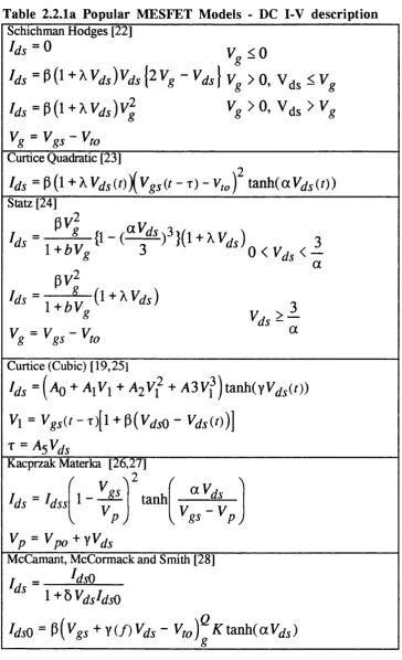
2 .2 .4 Review o f popular MESFET simulator models 37
2.2.4.1 Introduction to the Popular Simulator Models 37
2 .2 .4 .2 I-V Descriptions 39
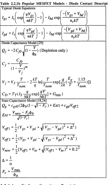
2 .2 .4 .3 Diode Law Descriptions 39
2 .2 .4 .4 Nonlinear Capacitance Descriptions 41
2 .2 .5 Introduction to the Parker Skellern Model 42
2 .2 .5 .1 The Parker Skellern Model 42
2 .2 .5 .2 The I-V Description 42
2 .2 .5 .6 Summary o f Parker Skellern Parameters 50
2 .2 .5 .7 Parameter Extraction Stratergy 51
2 .2 .5 .8 Features not included in the Parker Skellern Model 54
2 .2 .6 Simplified Models for Hand Analysis 55
2 .2 .6 .1 Square Law 55
2 .2 .6 .2 1-D Polynomial 55
2 .2 .6 .3 Adding Output Conductance to 1-D Polynomials 56
2 .2 .6 .4 2-D Polynomial 57
2 .2 .6 .5 Capacitor Model 57
2 .2 .7 Summary 58
2 .2 .8 References 58
2 . 3 N o n lin ea r A n alysis & M ea su rem en t 6 1
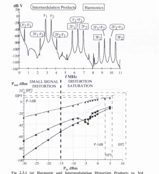
2 .3.1 Basic Definitions and Effects 61
2 .3 .1 .1 Harmonic and Intermodulation Distortion 61
2 .3 .1 .2 Distortion Saturation 62
2 .3 .1 .3 Spectral Spreading 63
2 .3 .1 .4 AM/PM Conversion 63
2 .3 .1 .5 Cross Modulation 64
2 .3 .1 .6 Inter-Symbol Interference and Bit Error Rate 64
2 .3 .1 .7 Linearity Specifications 64
2 .3 .2 Distortion Measurement 65
2 .3 .3 Distortion Analysis with Hand and Computer Aided Techniques 66
2 .3 .3 .1 Power Series 66
2 .3 .3 .2 Volterra Analysis 66
2 .3 .3 .3 Perturbation Method 67
2 .3 .3 .4 Harmonic Balance 67
2 .3 .3 .5 Variants 68
2 .3 .4 Frequency Dependant Distortion 68
2 .3 .5 Summary 68
2 .3 .6 References 69
2 . 4 L ow F req u en cy D esign T ech n iq u es 7 0
2.4.1 Linear Circuits 70
2 .4 .1 .1 OP-AMP Circuits 70
2 .4 .1 .2 Current Mode Circuits 72
2 .4 .2 Nonlinear Circuits 74
2 .4 .2 .1 Diode 74
2 .4 .2 .2 Differential Pair (Multi-tanh) 74
2 .4 .2 .3 Translinear Loop 75
2 .4 .2 .4 Gilbert Cell and Other Active 4 Quadrant Multipliers 76
2 .4 .2 .5 Bult & Haigh Toumazou Square Law Synthesis 77
2 .4 .2 .6 Precision Rectifiers 78
2 .4 .3 Summary 79
2 .4 .4 References 79
2 . 5 H ig h F req u en cy D esign T e ch n iq u es 8 1
2.5.1 Narrowband Circuits 81
2 .5 .1 .1 Matching Networks 81
2 .5 .1 .2 Transmission Line Hybrids 82
2 .5 .2 Wideband Circuits 82
2 .5 .2 .1 Wideband Baiuns 82
2 .5 .2 .2 Wideband Matching Networks 83
2 .5 .3 .1 Matched Amplifiers 84
2 .5 .3 .2 Low Noise Amplifiers 84
2 .5 .3 .3 Power Amplifiers 85
2 .5 .4 Nonlinear Circuits 86
2 .5 .4 .1 Mixers and Frequency Doublers. 86
2 .5 .5 Summary 87
2 .5 .6 References 87
2,.6 C om m on P ractical L in ea r isa tio n S tra teg ie s 8 9
2 .6 .1 Introduction 89
2 .6 .2 Output Back O ff 89
2 .6 .3 Feed Forward 89
2 .6 .4 Negative Feedback 91
2 .6 .5 Cartesian Feedback 91
2 .6 .6 Pre-distortion (Inverse Function Loads) 93
2 .6 .7 Balanced Structures 95
2 .6 .8 Filtering 96
2 .6 .9 Biasing 96
2 .6 .1 0 Addition o f linear components 97
2.6.11 Specially Doped Near Linear Devices 98
2 .6 .1 2 Summary 99
2 .6 .1 3 References 99
3
Device Circuit Interaction
1 0 13
.1
G e n era l 1 0 13 .2 E x a m p les o f N o n lin ea rities in L in ea r N etw o rk s 1 0 1
3.2.1 Nonlinear Conductance in Series with Resistor 101
3 .2 .2 Nonlinear Capacitance in Series with Resistor 104
3 .2 .3 Effect o f Amplitude - Validity o f Volterra and SPICE Analysis 105
3 .2 .4 Common Gate Amplifier 108
3 .2 .5 Current Mirror 109
3 .2 .6 Cascode Amplifier 110
3 .2 .7 Common Source Amplifier 111
3 .2 .8 Matching Networks 113
3 .3 D ev ice C ircu it In teraction A n a ly sis 1 1 4
3.3.1 A Simplified Common Topology 114
3 .3 .2 Generalised Analysis 115
3 .4 C o m p a riso n o f an alysis w ith r e a listic sim u la tio n 1 1 8
3 .5 S u m m a ry 1 1 9
3 .6 R e f e r e n c e s 1 1 9
Experience of Designing Haigh Toumazou
Square Law Circuits with Intermediate
Models of the MESFET
120
4 .2 .2 Numerical Medium Frequency Optimisation 121
4 .2 .3 Evaluation o f the Algebraic Optimisation 124
4 . 3 H ig h F req u en cy D isto rtio n in an A ctiv e Iso la to r 1 2 5
4.3 .1 Isolator Summary 125
4 .3 .2 Distortion mechanisms in the Isolator at high frequencies 125
4 .3 .3 Distortion Reduction by Phase matching 127
4 .3 .4 Distortion Reduction by Phase Restoration 127
4 . 4 T h e F req u en cy D ou b ler 1 2 8
4 .4 .1 Elimination o f the Fundamental at Medium Frequency 129
4 .4 .2 Elimination o f the 3rd Harmonic 130
4 .4 .3 Improving High Frequency Performance 131
4 . 5 M ea su rem en ts on a p rototyp e M M IC F re q u en cy D oub ler 1 3 2
4 . 6 S u m m a ry 1 3 3
4 . 7 R e fe r e n c e s 1 3 4
5
Distortion Nulling In the Single Common
Source MESFET
135
5 .1 In tr o d u c tio n 1 3 5
5 . 2 E ffect o f V o lta g e G ain 1 3 5
5 . 3 D isto rtio n N u llin g w ith 2 T erm 1 3 8
5 . 4 D isto rtio n N u llin g w ith 3 T erm 1 3 8
5 . 5 C om p arison o f th e P ark er Skellern M o d el w ith M easured
R e s u lt s 1 3 8
5.5.1 Triode Region 139
5 .5 .2 Saturated Region 140
5 . 6 B eh a v io u r o f O th er M od els 1 4 1
5 . 7 S u m m a ry 1 4 5
5 . 8 R e f e r e n c e s 1 4 6
6
A Derivative Based MESFET Synthesis
Technique Exploiting Real Device
Behaviour
147
6 .1 Ideal D eriv a tiv es S tru ctu res o f S elected C ir c u its 1 4 8
6.1.1 The ideal derivatives o f a linear amphfier 149
6 .1 .2 The ideal derivatives o f an active mixer 149
6 .1 .3 The ideal derivatives o f a limiter 150
6 . 2 D eriv a tiv e S u p erp o sitio n - A N o v el C ir cu it S y n th esis
T e c h n iq u e 1 5 0
6 . 3 L in ear Law 1 5 2
6 . 4 S q u are L aw 1 5 4
6 . 5 L im iter (H y p erb o lic Tan) 1 5 5
6 . 8 S en sitiv ity to P ro cess and T em p era tu re 1 5 7
6 . 9 S u m m ary 1 5 7
6 . 1 0 R e fe r e n c e s 1 5 8
7
Distortion Reduction Using 2 MESFETs
159
7 .1 In tr o d u ctio n 1 5 9
7 . 2 S im u la ted E x p lo ra tio n 1 5 9
7 . 3 T est J ig D escrip tio n 1 6 4
7 . 4 M easu red B eh a v io u r w ith B ias 1 6 5
7 . 5 C om p arison o f M ea su red D ynam ic R ange 1 6 8
7 . 6 S u m m ary 1 6 9
7 . 6 R e fe r e n c e s 1 6 9
8
Conclusions
170
8 . 1 C o n c lu s io n s 1 7 0
8 . 2 Future W ork 1 7 1
9
Publications and Associated Project
Supervision
173
9 .1 Papers and T u to ria ls P ublished by the A u th o r 1 7 3
9 . 2 W ork S u pervised by the A uthor 1 7 4
List of Fi£ures
C h ap ter 2S ectio n 2 . 1 G alliu m A rsen id e (G aA s) T e c h n o lo g y
Fig 2 .1 .1 (a) Single finger MESFET (b) Multi finger MESFET with through
substrate vias (not drawn to scale)
Fig 2 .1 .2 Transmission line structures using (a) Microstrip and Thin Film Microstrip (with via holes) (b) Coplanar and Slot lines (with air bridges).
Fig 2 .1 .3 MMIC capacitors (a) Parallel plate (b) Interdigital Fig 2 .1 .4 Planar Spiral Inductor
Fig 2 .1 .5 (a) Typical Energy diagram o f a pseudomorphic (PM) HEMT.
Physical structure o f PM HEMTs (b) AlGaAs GaAs (c) InALAs InP S ectio n 2 . 2 C haracterisation and M o d e llin g G aA s M E S F E T s
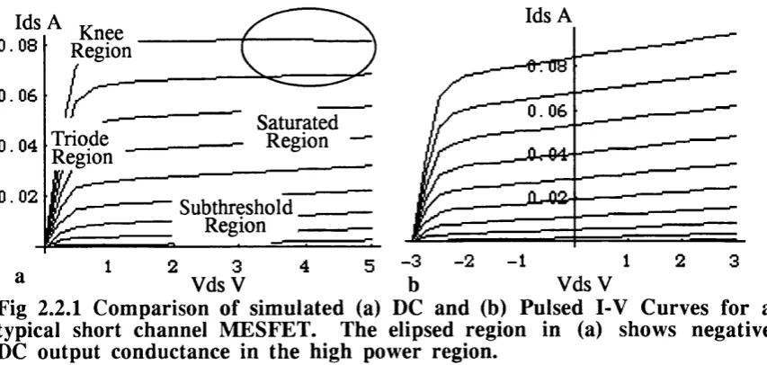
Fig 2 .2 .1 Comparison o f simulated (a) DC and (b) Pulsed I-V Curves for a
typicd short channel MESFET. The elipsed region in (a) show s
negative DC output conductance in the high power region.
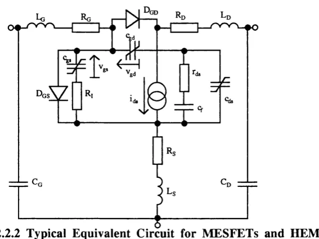
Fig 2 .2 .2 Typical Equivalent Circuit for MESFETs and HEMTs
Fig 2 .2 .3 Comparison o f simulated pulsed I-V Characteristics (relative to a fixed bias point) (a) Observed (represented by the Parker Skellern Model), (b) typical RC output conductance quick fix.
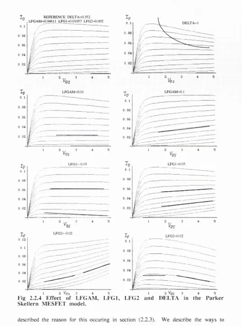
Fig 2 .2 .4 Effect o f LEG AM, L F G l, LFG2 and DELTA in the Parker Skellern MESFET model.
Fig 2 .2 .5 (a) Effect o f VST on the softness o f pinchoff (b) The usefulness o f VST in predicting the IM3 minimum near pinch o ff
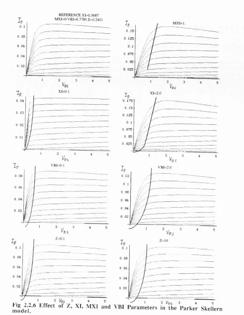
Fig 2 .2 .6 Effect o f Z, XI, MXI and VBI in the Parker Skellern model.
Fig 2 .2 .7 Simulated Schottky Contact behaviour o f the Parker Skellern model (a) Gate Leakage Current, (b) Gate Drain Breakdown
Fig 2 .2 .8 Simulated (a) Cgs (fF) (b) Cgd (fF) for the MGF1400 MESFET using
the Parker Skellern version o f the Statz capacitance model.
Fig 2 .2 .9 The Parker Skellern version o f the Statz Capacitance model for the MGF1400 (a) Effect o f FC, (b) Effect o f XC
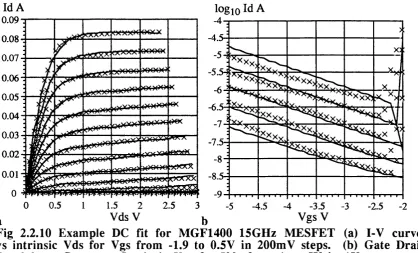
Fig 2 .2 .1 0 Example DC fit for MGF1400 15GHz MESFET (a) I-V curves vs
intrinsic Vds. (b) Gate Drain Breakdown Curves vs V gs. S ectio n 2 . 3 N o n lin ea r A n a ly sis & M ea su rem en t
Fig 2 .3 .1 (a) Harmonic and Intermodulation Distortion Products to 3rd order, (b) Small Signal Distortion, Intercept points and Distortion Saturation Fig 2 .3 .2 In a band limited modulated signal, the nonlinearity o f a power
amplifier has the effect o f regenerating the side lobes. S e ctio n 2 . 4 L ow F requ en cy D esign T e c h n iq u e s
Fig 2 .4.1 (a) Simplified Schematic o f the BIT OP Amp (b) GaAs OP Amp
Fig 2 .4 .2 Selected OP-Amp Circuits (a) Noninverting Amplifier (filter),
(b) Transconductance (Voltage Regulator) (c) Inverting Amplifier (filter) and Transimpedance (d) Switched Capacitor Filter
Fig 2 .4 .3 A selection o f implementations o f the Current Conveyor.
Fig 2 .4 .5 Piecewise Linear Approximation using Diodes (a) Example Circuit (b) Idealised Transfer Characteristic
Fig 2 .4 .6 (a) Single BIT Differential Pair (b) "Multi-Tanh" Triangle to Sine Converter based on multiple BIT Etifferential Pair.
Fig 2 .4 .7 (a) The Translinear Principle, the diode loop, (b) The Translinear Loop Frequency Doubler.
Fig 2 .4 .8 (a) The Basic Gilbert Cell (b) FET 4 Quadrant mixer.
Fig 2 .4 .9 Square Law Synthesised Circuits (a) & (b) Bult, (c) & (d) Haigh & Toumazou's
Fig 2 .4 .1 0 Selected Precision Rectifiers
S ectio n 2 . 5 H ig h F req u en cy D esig n T e c h n iq u e s
Fig 2 .5 .1 Examples o f RF impedance matching to the input o f a FET using (a) LumpW Elements, (b) Distributed Elements.
Fig 2 .5 .2 Branch Line Hybrid.
Fig. 2 .5 .3 The Transformer Hybrid.
Fig 2 .5 .4 The Distributed Amplifier.
Fig 2 .5 .5 Design o f a Low N oise Amplifier.
Fig 2 .5 .6 FET Mixer Configurations.
S ection 2 . 6 C om m on P ractical L in ea risa tio n S t r a t e g ie s
Fig 2 .6.1 (a) Feed Forward System (b) Negative Feedback System
Fig 2 .6 .2 Cartesian Feedback Linearisation
Fig 2 .6 .3 The Voltage Inverter
Fig 2 .6 .4 Adaptive Baseband Predistortion
Fig 2 .6 .5 The basic balanced structure.
Fig 2 .6 .6 Variation o f IM3 (dBm) with V gs bias
Fig 2 .6 .7 Balmford & Redman-White low distortion current mirror
Fig 2 .6 .8 Measurements o f intermodulation distortion for a MGF1400 MESFET
vs Load Resistance C hanter 3
Fig 3.1 (a) Circuit with Nonlinear Conductance, (b) Circuit with Nonlinear
Capacitance
Fig 3.2 Harmonic Distortion in voltage and current vs Resistance for a
Nonlinear Conductance in series with a linear resistance.
Fig 3.3 Harmonic Distortion in voltage and current vs Frequency for a
Nonlinear Capacitance in series with a linear resistance.
Fig 3.4 Distortion in the voltage across a nonlinear component in series with a
resistor (a) for nonlinear capacitance as frequency is varied for (i) 0.1 Vpk and (ii) IVpk. (b) Distortion as the level o f excitation is varied for (i) nonlinear conductance (ii) nonlinear capacitance, (c) Spectrum o f distortion as amplitude is varied showing "skirts" (d) Spectrum o f distortion as the length o f simulation is increased also showing "skirts".
Fig 3.5 (a) Common Gate, (b) Common Gate - Current Mirror Equivalence (c)
Cascode (d) Common Source
Fig 3 .6 Distortion in the Common Gate circuit v s real and imaginary parts o f Y
Fig 3.7 Distortion in gate source (a) voltage and (b) drain current for Cascode circuit vs real and imaginary parts o f Y.
Fig 3.8 Distortion in gate-source voltage and drain current for the Common
Source circuit vs Rs and frequency.
Fig 3.9 Matching Networks: Narrow band "L section" (a) Rg > Rs (b) Rg < Rs; (c) Wideband "Transmission Line".
Fig 3 .10 Narrow band "L-section" matching network with nonlinear capacitor, (a) distortion in voltage, (b) distortion in current.
Fig 3.11 Wideband "transmission line" matching network with nonlinear
capacitor, (a) distortion in voltage, (b) distortion in current.
Fig 3.12 The nonlinear element embedded in a linear network.
Fig 3.13 Comparison o f distortion in v and i for cascode using simple Volterra analysis with simulation using Parker-Skellem model
Fig 3.14 Distortion vs Frequency in the current driven common gate circuit, (a) vgs, (b) ids.
C hap ter 4
Fig 4.1 (a) The Voltage Inverter (b) The loaded 4 FET transconductor.
Fig 4 .2 Effect o f g 1 on (a) k, (b) w, (c) Av with different R l and y
Fig 4.3 (a) R-w compensated isolator (b) Phase restored compensated isolator
Fig 4 .4 (a) Comparison o f R-w (Phase Matched) compensated (IGHz) and w
compensated Isolator (b) Comparison o f Phase Restored compensated (IG H z) and w compensated Isolator
Fig 4 .5 (a) Frequency Doubler with Voltage Inverter stage (b) Variation o f the
basic Frequency Doubler with a Self-Conductor Input
Fig 4 .6 (a) Distortion versus frequency for different Load Resistance for the Frequency Doubler with Self-Conductor Input (b) Comparison o f Voltage Inverter and Self-Conductor Frequency Doubler performance
Fig 4 .7 MMIC Layout o f Frequency Doublers, (a) High Impedance Input
form with active resistor input termination, (b) Self-conductor input form.
Fig 4 .8 Measured performance o f a "self conductor" Frequency Doubler. (a) Power Sweep, (b) Frequency Sweep, (c) Vds Sweep, (d) Frequency Sweep at optimum Vds.
C hanter 5
Fig 5.1 Input referred distortion vs relative voltage gain (a) contribution o f each nonlinear term in the 2D Taylor Series; 2 Dominant terms (b) no null, (c) narrow deep null; 3 Dominant terms (d) shallow null, (e) wide deep null, (f) double narrow deep null.
Fig 5 .2 Distortion in the Common Source M G F1400 MESFET in the Triode
Region. Simulations with the Parker Skellern MESFET model o f (a) 2nd and (b) 3rd order input referred harmonic distortion vs gate bias and load resistance. Comparison o f measured and simulated (c) 2nd (d) 3rd order output referred intermodulation distortion .
Fig 5.3 Distortion in the Common Source M G F1400 MESFET in the
Saturated Region. Simulations with the Parker Skellern MESFET
model o f (a) 2nd and (b) 3rd order input referred harmonic distortion
vs gate bas and load resistance. Comparison o f measured and
Fig 5 .4 Simulated variation o f the 2nd Harmonic with gate bias and load resistance o f the M GF1400 Triode Region for (a) Tajima (b) TOM (c) Curtice (d) Materka.
Fig 5.5 Simulated variation o f the 3rd Harmonic with gate bias and load
resistance o f the M GF1400 Triode Region for (a) Tajima (b) TOM (c) Curtice (d) Materka.
Fig 5 .6 Simulated variation o f the 2nd Harmonic with gate bias and load resistance o f the M GF1400 Saturated Region for (a) Tajima (b) TOM (c) Curtice (d) Materka.
Fig 5.7 Simulated variation o f the 3rd Harmonic with gate bias and load
resistance o f the M GF1400 Saturated Region for (a) Tajima (b) TOM (c) Curtice (d) Materka.
C han ter 6
Fig 6.1 (a) Derivatives o f an Ideal Amplifier (b) Derivatives o f an Ideal Multiplying MixCT
Fig 6.2 (a) Derivatives o f the ideal Limiter (b) Derivative structure o f a real MESFET derived from the Parker Skellern model.
Fig 6.3 Topology for derivative superposition.
Fig 6.4 Linear Law Approximation using Derivative Superposition. The RF
derivatives are plotted against DC V gs Voltage.
Fig 6.5 (a) g3 and (b) g2 derivatives vs bias for Square Law approximation.
Fig 6 .6 SPICE Simulation o f limiter circuit. (a) Dynamic transfer
characteristic, (b) Approximately sinusoidal output under triangular excitation.
Fig 6.7 (a) SPICE Simulation o f the dynamic transfer characteristics o f
derivative superposition based frequency doubler, (b) Time domain simulation o f the frequency doubler under sinusoidal drive conditions
Fig 6.8 (a) SPICE Simulation o f the dynamic transfer characteristics o f
derivative superposition based frequency tripler, (b) Time domain simulation o f the frequency doubler under sinusoidal drive conditions C hapter 7
Fig 7.1 (a) The simplified 2 FET system (b) Modified form.
Fig 7.2 Magnitude o f the distortion for two MESFETs as the gate bias o f the secondary FET is varied whilst the main MESFET is held constant.
Fig 7.3 Using a secondary MESFET to produce near simultaneous 2nd and
3rd order distortion nulls.
Fig 7 .4 Exploration o f the composite transconductance derivatives o f 2 FETs with bias for different width ratios.
Fig 7.5 Schematic o f the Linear Law Demonstration Board.
Fig 7 .6 Synthesised (a) 2nd Order & (b) 3rd Order derivatives.
Fig 7.7 Bias dependant distortion synthesised with 2 FETs for different gate
bias, simulated with (A) TOM (transconductance nonlinearity only) (B) Parker Skellern (transconductance nonlinearity only) (C) Full Parker Skellern Model (D) Measured Performance.
List o f Tables
C han ter 2Table 2 .2 . la Table 2 .2 . lb Table 2 .2 .2
Table 2 .2 .3
Table 2 .3 .1 C han ter 3 Table 3.1 C han ter 4 Table 4.1
Table 4 .2
Popular MESFET Models - DC I-V description
Popular MESFET Models - Diode Contact Description
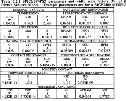
SPICE3F4PS2 parameters and width scale factors (W) o f the Parker Skellern Model. (Example parameters are for a MGF14(X) MESFET) Extrinsic Volterra Parameters o f MESFET models and pulse measurements o f the FET in Fig 2 .
Summary O f Non-Linear Analysis Techniques
Y and AS Parameters for Som e Common Circuits
Comparison o f calculated and simulated widths for R l= 2 5 and Y=0.044.
1
Introduction
1 .1 A im s o f th is T h esis
This project attempts to develop a circuit design methodology for designing MMIC circuits with low distortion to realise linear and nonlinear functions using the Parker Skellern MESFET Model. In Section 1.2 we briefly describe the role o f GaAs technology and the difficulties that have been encountered. In Section 1.3 w e describe the structure o f this thesis.
1 . 2 A p p lica tio n o f G aA s C ircu its and M o tiv a tio n fo r th is T h esis
GaAs technology has taken a long time to come o f age, compared to the rapid growth o f the s ilicon industry. However, GaAs has a unique niche in the RF market, providing a reliable and relatively straight forward medium for realising Monohthic Microwave Integrated Circuits (MMICs). Silicon remains strongly competitive in terms o f high frequency performance, but it is much harder to utihse that performance in the MMIC environment. This has led to a viable market for GaAs in mobile communication systems, satellite systems and other high frequency systems in the l-60G H z region. GaAs has been problematical to use due to the lack o f rehable simulator models and the lack o f circuit techniques to exploit its high speed. Whilst s-parameter measurements were commonly used to overcome the problems associated with small signal design, the area o f predicting distortion with device models was frequently abandoned. In the past few years high quality
MESFET models have begun to emerge, capable o f giving valuable insight into the nonlinear behaviour o f circuits and for the first time. This has started to lead to reliable optimisation for low distortion. Reliable prediction and minimisation o f distortion can be a
to concentrate on very high frequencies due to the outstanding success o f silicon at frequencies up to about 900MHz.
1 . 3 W ork P resen ted in th is T h esis
This thesis addresses the area o f circuit design using GaAs MESFETs, concentrating on obtaining precision nonlinear behaviour. This work exploits pioneering work carried out by Dr Anthony Parker on developing a high quality MESFET model for nonlinear simulation, the Parker Skellern MESFET model. The work extends circuit theoretical work
begun by Dr David Haigh and Dr Chris Toumazou. The work ends by exploiting a
detailed knowledge o f the Parker Skellern model to verify and predict distortion reduction schemes involving one or more devices that are not possible to predict from simple circuit theory or other common simulator models.
The work presented in this thesis is divided into a number o f sections including an extensive background for this work (Chapter 2), followed by a study o f basic distortion mechanisms arising from the interaction o f the device nonlinearity with its associated circuit and parasitics (Chapter 3), the application o f simple and complex device models for multi-FET circuit analysis (Chapter 4), study o f distortion nulling effects in an amplifier with load resistance and bias (Chapter 5), a novel derivative superposition based circuit synthesis technique is presented (Chapter 6), followed by an evaluation o f this technique in a two device circuit (Chapter 7). References are given at the end o f each chapter. We then draw general conclusions from this work (Chapter 8). Finally w e list papers that have been written by the author and projects the author has been involved in (Chapter 9). W e now
describe in more detail the contents o f the chapters.
provides a detailed description o f the Parker Skellern MESFET model, a state o f the art model used through out this thesis for accurate simulations. It also includes useful approximations o f device m odels suitable for hand analysis. 2.3 provides an introduction to nonlinear behaviour including distortion measurement and analysis techniques and tools. 2.4 reviews the main design approaches available for low frequency design, including linear and nonlinear circuit design techniques for both silicon and GaAs. 2.5 reviews the main design approaches used for high frequency design including techniques used for both wide and narrowband circuit design. 2.6 reviews linearisation techniques for nearly linear
circuits such as feedforward and balancing. In this chapter references are given at the end o f each section.
C hap ter 3: This chapter examines the phenomenon that numerous circuits are prone to significant levels o f frequency dependant 3rd order distortion even when containing an ideal simple square law device. W e call this effect Device Circuit Interaction. W e show a common relationship between circuits suffering from Device Circuit Interaction and give a simple design rule for determining if the distortion is likely to be near a maximum. W e also show that Device Circuit Interaction also shows that distortion is sensitive to resistive components, giving a valuable insight into negative feedback. Finally w e show the relationship between the simple D evice Circuit Interaction predictions and those predicted with the Parker Skellern MESFET model.
C hap ter 4: This chapter attempts to analyse and correct key weaknesses o f the Haigh Toumazou "square law" MESFET synthesis technique. The work studies the attenuation and the contamination o f key drive signal through electrostatic feedback (output conductance). W e show that the electrostatic feedback problem can be corrected by altering device widths. We also apply our idea o f Device Circuit Interaction, showing the presence
measurements on a frequency dependant distortion resistant Frequency Doubler circuit built with the GEC F20 process.
C h a p ter 5: This chapter builds on existing experimental work by Parker & Scott on distortion nulling in the common source with load resistance. W e give a detailed graphical explanation o f how the distortion behaviour varies with load resistance. Follow ed by a systematic study o f the bias and load resistance dependence o f the distortion with the Parker Skellern model, including measured results and a comparison with other simulator models. W e conclude that this distortion nulling behaviour to be sufficiently sensitive as to provide a unique tool for model vahdation. We show that although the Parker Skellern MESFET model is not perfect for predicting load dependant distortion, it is an order o f magnitude better than other common simulator models.
C h a p ter 6: The high level o f realism o f the Parker Skellern MESFET model allows us to predict with a reasonable level o f confidence, the dynamic (RF) derivatives o f a device. In this chapter we use these realistic derivatives to develop a novel circuit synthesis technique based on the superposition o f transconductance derivatives in the voltage domain to reahse arbitrary transfer functions. The technique is illustrated using the derivatives o f typical MESFETs to generate a wide range o f functions including Linear Law approximation. Square Law approximation, frequency doubler and tripler, and a hmiter (triangle to sine).
C h a p ter 7: In this chapter we attempt to verify the validity o f the derivative based nonhnear circuit synthesis proposed in Chapter 6. A first order approximation to the Linear Law o f Chapter 6 can be produced with only two devices. A version o f this circuit was
realised using discrete MESFETs and the distortion behaviour was mapped. This
demonstrator confirmed the underlying idea o f Chapter 7 and showed additional degrees o f freedom by using different bias points. The demonstrator warns o f the sensitivity to high load resistance which we are able to confirm through a detailed Volterra analysis.
C h a p ter 8: In this chapter w e draw conclusions from the areas described.
2
Background
In this chapter w e present a description o f the current engineering framework into which the work presented in subsequent chapters fit. At a practical level, analogue circuit design, particularly at higher frequencies is inseparable from the technology that it is to be implemented in and CAD tools to develop the designs with.
We begin by describing the technology to be used in circuit design, which w e assume is
GaAs MMIC based. Next w e consider the modelling o f the FETs used in MMIC
technology with an emphasis on the Parker Skellern MESFET model. Then w e describe Nonhnear Measurement and Analysis techniques. After this w e describe the circuit
techniques used at low and high frequencies and the techniques used to hnearise these circuits.
The treatment o f the material in this chapter is generally kept to a relatively superficial level with the exception o f Device Modelhng, which is considered o f such fundamental importance to large signal circuit design, that a more detailed discussion is given.
2 . 1 G a lliu m A rsen id e (G aA s) T e ch n o lo g y
Galhum Arsenide (GaAs) based technology has slowly developed over the past 30 years [1]. Experimental FETs with gate lengths o f 24pm were demonstrated in the mid 1960's at the GEC-Caswell research centre. The first commercial 4pm MESFET (GATl) appearing in 1970 from Caswell with lOdB o f gain at IGHz. In 1971 a 1pm gate length was demonstrated with a prototype Electron-beam lithography system and led to a commercial MESFET in 1973 (GAT3).
III-V Technology has continued to grow, embracing new processing steps such as Molecular Beam lithography which allows layers o f a few molecules thick to be grown on a substrate. Dry etching techniques which selectively etch III-V materials, and in some
cases, etch in predominantly one direction. Various kinds o f Hetrostructure based devices have emerged based on growing Pseudomorphic structures (i.e. a structure made o f different chemical layers that have a compatible crystallographic structure and lattice spacing). These have included the High Electron Mobility Transistor (HEMT) and the Hetrojunction Bipolar Transistor.
In this section we review the properties o f GaAs as a substrate. W e examine the structure o f a typical GaAs MESFET. W e review typical MMIC foundry components including interconnections, transmission lines, capacitors, inductors and resistors. W e then describe the external connections to a typical MMIC. Finally w e look at HEMTs, HBTs and future technologies for implementing these and other devices.
2 . 1 . 1 P ro p erties o f th e G aA s S u bstrate
Whilst both Silicon and GaAs are semiconductor materials, they differ significant)!^. We briefly state the important differences and elude to their significance.
Silicon is often quoted as being significantly cheaper than GaAs. In practice things are much less straight forward. Silicon foundries are mainly interested in high volume production (digital) runs making small quantity designs financially unattractive. Many o f the advanced Silicon processes are expensive, especially Bi-CMOS processes, due to the complexity o f the fabrication process and the small feature size. Gallium Arsenide economically favours small production runs, and many o f the MESFET processes have very simple fabrication requirements, together with a w ell characterised analogue design library.
layer is that o f the wafer (typically 2(X))Lim). This leads to relatively large stray fields
be
requiring components to be well spaced out if lengthy field simulations are to^ avoided. However there is very low stray capacitance to the conductive back plane.
In Silicon the energy gap is relatively low, making the intrinsic semiconductor relatively conductive due to a lower energy gap. Component isolation is obtained by light doping o f the substrate and forming protective pn junctions. The pn junction is very thin and leads to significant stay capacitance to the conductive substrate. The thinness o f the pn junction greatly reduces stray fields allowing a high density o f integration. At microwave frequencies this increase in circuit density can be difficult to utilise due to the penalty in stray capacitance. This effect is most pronounced in spiral inductors fabricated on a silicon substrate. To overcome this interest has grown in "Silicon on Insulator" processes, where the active device is fabricated on a layer o f insulator. [2,3]
GaAs has a lower thermal conductivity than Silicon limiting the maximum power that can be handled on a chip. This problem may be eased with the development o f novel heat sinking techniques such as the GMMT "Bath Tub" process, where the wafer is locally thinned under a FET and the spaced is filled with gold [4].
Another advantage o f GaAs is the nature o f its photoelectric behaviour. In silicon, for an electron to be transferred from the valence band to the conduction band it must not only absorb a photon, but also obtain a certain velocity. This requires the presence o f photons and fortuitous thermal agitation. [5, 6] Similarly for photo emission, the electron must
The higher energy gap o f GaAs and InP compared to Silicon and Germanium leads to lower noise from thermal ionisation's in the bulk and a greater resilience to ionisation from
external radiation sources (i.e. it is naturally radiation hard).
At low electric fields, a high electron mobihty exists in GaAs in all directions. In high electric fields the saturation velocity o f the electron is greatest in only one direction. In order to obtain the highest frequency performance from an active device, the orientation o f the active devices is aligned to this high saturation velocity axes o f the crystal. Directionahty in saturation velocity also exists in Silicon, but this is not referred to in the
context o f device alignment.
The mobility o f holes in GaAs is much less than that o f electrons and this leads to significantly slower devices (around an order o f magnitude slower). Since GaAs is targeted at the higher frequency market, p type devices are not normally encountered. In Silicon the difference between hole and electron mobility is less. The Silicon market includes low frequency designs where ultimate speed performance is not generally required. This has led to the development o f complementary technologies such as CMOS and Bipolar, where the reduction in speed is more than offset by the flexibility and ease o f design. At very high frequencies, n type silicon devices are only used.
2 . 1 . 2 S tru ctu re o f a typ ical M E S F E T
a
Fig 2.1.1 (a) Single finger M ESFET (b) M ulti fin ger M E SF E T with th rou gh su bstrate vias (not drawn to scale)
source channel and reduces the device current. Apart from leakage currents, the depletion
region is capacitve in nature.
The very thin gate stripe has a tendency to form a lossy RC transmission line. This sets a
limit on how wide a FET should be without degrading its frequency response (typically 70-
100pm). (With very thin gates, a mushroom gate shape is preferred to reduce the loss).
To overcome this limitation, multi-finger topologies such as that shown in Fig 2.1.1b have
been developed where the drain and source contacts o f one FET finger are merged with
those o f their neighbours. The use o f multi-finger EETs can present problems for
characterisation. The inner fingers of the EET tend to work at a higher temperature than the
outer fingers [8]. Some of the drain and source contacts are shared, and the contact
resistances are not the same as for the single finger FET. The additional overlap between
gate and source metalization leads to increased parasitic capacitance.
2 . 1 . 3 P assive MMI C C om ponents
In a typical MMIC foundry process, there are a wide range o f passive components
available, these include interconnections, lumped elements such as capacitors, inductors,
resistors as well as distributed elements made from transmission lines. These structures are
carefully characterised by the manufacturer leading to detailed foundry guides and library
support for popular simulator and layout packages such as MDS and Cadence. There are
generally restrictions on some of the dimensions o f the com ponents due to limits on what
SLOT D VIA
THIN FILM
CPW STD
S VIA
F ig 2.1.2 T ra n s m is sio n lin e s tr u c tu r e s u sin g (a) M ic r o s tr ip a n d T h in F ilm M ic ro s trip (w ith via holes) (b) C o p la n a r a n d S lot lines (w ith a ir b rid g es).
guidelines are detailed in the foundry guide. In the preparation o f this section, extensive
reference has been made of foundry guide material supplied by GM M T F20 [9] and
Fraunhofer [ 10] through Eurochip (Now called Europractice).
I n te r c o n n e c tio n s : Interconnections between the various components are achieved by
using two metal layers. These are separated either by air bridges (e.g. Fraunhofer process)
or a dielectric layer (e.g. GMM T process). The back o f a chip is usually coated with metal
(forming a ground plane) and some processes allow electrical connection to this layer using
"through substrate vias" filled with metal to reduce parasitic resistance and inductance and
resistive noise generation (e.g. GMM T process). The "through substrate via" weakens the
strength of the chip and the minimum spacing between successive vias is strictly limited.
We illustrate the different kinds o f interconnection in Fig 2.1.2.
T ra n s m is s io n L in es: At frequencies above about 5GHz, the implementation of
transmission lines on a MMIC chip becomes an attractive design technique. The type o f
transmission lines available is restricted by the interconnection strategy o f the foundry and
what characterisation work has been carried out by the foundry. (If a technique is possible
with a given foundry process but has not been characterised, considerable time, effort and
money would be needed to develop and characterise the technique which may be
unattractive in an industrial setting.) A detailed discussions on MMIC transmission lines
Fig 2.1.3 M M IC capacitors (a) Paral el plate (b) Interdigital
Four types o f transmission line are typically encountered in published MMIC designs.
These are the Microstrip Line, the Thin Film Microstrip Line, the Coplanar Line and the
Slot Line.
(i) The Micro strip transmission line (Fig 2.1.2.a) has a metal strip and a ground plane
separated by the insulating substrate. The characteristic impedance is determined by the
substrate thickness (fixed), the dielectric constant (fixed) and the track width (variable).
The back plane of the chip forms the ground plane (e.g. GMMT).
(ii) A variation on this is the thin film transmission line (Fig 2.1.2a) where the dielectric
layer between the two top metalizations forms the substrate and one o f the metalizations
forms a ground plane. This technique has less stray fields than the substrate form, and this
allows a more compact layout. This technique has been demonstrated with the GMMT F20
process by Robertson in [ 111 but is not currently supported by GMMT.
(iii) The coplanar wave guide (CPW ) (Fig 2.1.2b) [13] is a uniplanar technique consisting
o f a track and two ground planes (linked by the occasional air bridge etc). The
characteristic impedance is controlled by the width of the central track and the spacing
between the ground planes (e.g. Fraunhofer process). The CPW allows a constant
impedance to be achieved whilst changing from a large structure such as a RF input pad to a
small structure such as a FET gate (through a reduction in the line width and spacing).
(iv) The Slot line (Fig 2.1.2b) is also a uniplanar technique consists o f two large
conductive sheets where the characteristic impedance is determined by the slot width. This
Fig 2.1.4 Planar Spiral Inductor
line is described in detail by Gupta in [14] and demonstrated with the F20 process by
Robertson in [11]
C a p a c ito r s : There are usually two types o f lumped capacitors available in a typical
MMIC foundry processes. These are the metal insulator metal (MIM) capacitor (Fig
2.1.3a) for larger capacitors, and the interdigital capacitor (Fig 2.1.3b) for very small
capacitors. The capacitance is determined by the plate spacing, dielectric and plate area
(number o f fingers). For small capacitances, these capacitors contain a significant stray
capacitance to the ground plane and other components, which can affect filter design.
Inductors: Inductors are formed from planar spirals resting on the substrate giving inductors in the range of 3-15nFI (Fig 2.1.4). These inductors have com paratively high
series resistance due to the thin track making the spiral, limiting the Q factor. There is
significant stray capacitance both to ground and between the turns, limiting the self
resonance frequency and leading to possible spurious resonances. Foundry guides provide
detailed equivalent circuits for particular spacings and thickness and shapes o f the spirals.
Some foundries offer stacked spiral inductors (GMMT) and integrated transformers
(MACOM). The realisation of Spiral Inductors in silicon processes has been very difficult
due to the high substrate capacitance and eddy current losses in the substrate.
R e s i s t o r s : Resistors are formed either from lengths o f nichrome metalization (e.g. GM M T F40) (for resistors below Ik), or Mesa resistors (e.g. GMMT F20) formed from
Mesa resistors can exhibit significant nonlinearity if they have large electric field across them.
2 . 1 . 4 C o n n ectin g to th e O u tsid e W orld
Connecting to the outside world from a MMIC chip is a two stage process. The first part is the wiring from the active part o f the circuit to a bond pad. Then there are the connection from the bond pad to outside world.
For low frequency bias, the bond pad is simply a square o f metalization not covered by the passivation layer. For RF pads, a "coplanar launch" consisting o f a central RF pad and two
ground pads, carefully spaced to match to the 5 0 0 environment In the Microstrip environment the ground pads connect to substrate vias. In the CPW environment the ground pads are expanded to form the CPW structure.
There are two types o f outside connections. There is the temporary probing method, where needle probes are carefully placed on each pad on a probe station. The RF probe consists o f a coplanar structure that enlarges towards the connector. These probes are rather expensive (£lk-£5k) and are difficult to align with the chip. Alternatively the chip is mounted on a substrate and bond wires are welded to the bond pad and the tracks on the substrate.
At microwave frequencies the bond pads, bond wires, packaging etc. all have parasitic
impedances associated with them which should be included in the simulations. At
milhmetre frequencies, care has to be taken with grounding, else parasitic resonant modes can occur.
2 . 1 . 5 S tru ctu re o f a tvp ical H igh E lectro n M o b ility T ra n sisto r (H EM T)
Channel
Donor
Ec
/
Buffern-GaAs
n-AlGaAs Donor
i-AlGaAs Spacer
i-GaAs Buffer
N/
Substrate i-GaAs
n-InGaAs
n-InAlAs Donor
i-InGaAs Channel
i-InAlAs Buffer
Substrate i-InP
Fig 2.1.5 (a) T ypical E nergy diagram o f a pseu dom orp h ic H EM T.
Physical stru ctu re o f pseudom orphic H EM Ts (b) A lGa As Ga As based (c )
InAlAs In ? based. N ote M ushroom gates reduce gate resistan ce.
to defects in the crystal lattice structure resulting in trapping centres which can result in a
disparity between DC and RF performance.
In the HEMT [ 15] an attempt is made to separate the charge carriers away from their donor
atoms by providing a region at a lower energy level outside o f the donor area by fabricating
an undoped hetrojunction channel A hetrojunction is an interface between two materials of
differing energy gaps. A buffer layer is usually applied on the other side of the low energy
channel region to provide additional carrier confinement. The undoped nature o f this
hetrojunction channel results in a higher electron saturation velocity and low scattering.
Electron saturation velocity is further increased by selecting a spacer material with a high
electron mobility e.g. InGaAs. This leads to a higher transconductance and lower noise.
The charge carriers in the hetrojunction layer are usually referred to as a 2D Electron Gas
(2DEG). Due to the restrictions o f Quantum Mechanics, the hetrojunction can only store a
certain number o f charge carriers. The level in the Quantum Well is determined by the level
o f charge on the gate side o f the depletion region, a high gate charge (i.e. a negative bias)
leads to a low level o f charge in the Quantum Well. When the Quantum Well is full, the
carriers spill over into the donor and buffer regions. A simplified typical energy diagram of
the conduction band o f a H EM T is shown in Fig 2.1.5a, showing that the donated carriers
accumulate in the spacer layer. (At a simplistic level, the donated electrons can be thought
The types o f hetrojunctions can be loosely divided into the following systems AlGaAs GaAs[16], AlGaAs InGaAs [17] and the InAlAs InP[18] (Figs 2.5b& c). The AlGaAs
GaAs system has the advantage that both materials have the same lattices structure and lattice spacing, allowing any proportion o f A1 and Ga to be used, leading to little frequency dispersion. The InP system tends to only match with Ga and A1 systems when certain
ratios o f Ga A1 and In are used (giving rise to the term o f Lattice Matched HEMTs). W e w ill talk about InP in more detail in section 2.1.8.
The thinness o f the spacer layer is a limitation for power amplification. This has led to multiple hetrojunction layer devices [1 9 ,2 0 ].
2 . 1 . 6 He tr oj un ct i on B ip o la r T ra n sisto rs (H B T s)
In recent years, interest has been growing in the development o f Hetrojunction Bipolar Transistors. As in the HEMT, these devices appear to offer lower noise and higher speed devices. Much is made o f the high power efficiency o f HBTs [21], although the problem o f heat sinking in GaAs HBTs has largely been undiscussed in the literature. HBTs have for a long time been unavailable in Europe as a MMIC process, but GMMT is setting up a HBT foundry process. Since this thesis is restricted to MESFETs, w e do not consider the HBT further in this thesis.
2 . 1 . 7 F u tu re T ech n o lo g ies
Various technologies for making HBT and FETs appear in the electronic press and these have included Silicon Germanium (SiGe), Indium Phosphide (InP), Diamond and Silicon
Carbide (SiC). SiGe Hetrojunction HBT and MOSFET technology [22,23] offers
improved transconductance and speed over conventional Silicon. InP EiEMTs with device
order greater than GaAs). The author believes that the processing for these materials has some way to go before MMICs can be routinely fabricated.
A range o f Quantum Mechanical devices have appeared. Perhaps the most interesting is the
Resonant Tunnelling Transistors, which hold the possibility o f high transconductance and very high frequencies o f operation [28], although the i-v characteristic look rather erratic.
There is also interest in developing GaAs processes for use at high temperature [29]
2 . 1 . 8 S u m m a ry
In this section w e have seen that Silicon and GaAs have quite different properties as a substrate. After a long development time, GaAs now offers a substrate on which MMIC circuits can be built including a range o f transmission line structures and lumped passive elements. There is a great diversity in device type and size ranging from 0.7jum MESFETs to 0.1 pm state o f the art HEMTs, but seldom in the same process. This points to the need to be able to design circuits that exploit the behaviour o f the technology to the full whilst minimising the number of chips to realise a practical system. There is considerable research into alternative materials for realising high frequency FETs, some o f which may exhibit similar device behaviour to existing MESFET and HEMT foundry processes.
2 . 1 . 9 R e fe r e n c e s
1 J .Turner, History of FaAs FET at Caswell (1964-1985), I EE Colloquium on Modelling, Design and Application of MMICs, 17th June 1994, ppl/1-1/3.
2 P.H.Saul, The Benefits of Bonding lEE Review November 1994, pp. 263-266.
3 P.H.Saul, The Bonded Wafer Silicon on Insulator Approach to High Performance Low Power Integrated Circuits, lEE Colloquium on "Advanced MOS and Bipolar Devices", February 1995, Digest No
1995/033.
4 R.Eaton and F.A.Myers, Technology, Circuit Design and Applications of GaAs MMICs, lEE Electronics and Communications Journal Dec. 1990 Vol. 2, No. 6, pp233-243. (1-100).
5 SJ.Rossek, C.E.Free, Optical Control of Microwave Signals Using GaAs FETs, lEE Electronics & Communications Journal, Vol. 6, No. 2, Feb 1994, pp2I-30
6 A.H.KaIid, S.A.Bashar, A.A.Rezazadeh, Fabrication and Characterisation of a transparent Gate HEMT using Indium Tin Oxide, IEEE EDMO Oct 1994, London pp99-104.
7 C.Hardingham, GaAs Space Solar Cells, IEEE EDMO Oct 1993, London. 8 M.Darvishzadeh, PhD Thesis^
10 lAF Design Manual (Fraunhofer Institute Foundry Guide) Version 3.0 March 1 1994
11 M.Gilhck, I.D.Robertson, A JlA ghvam i, Uniplanar techniques for Monolithic Microwave Integrated Circuits, lEE Electronics & Conununications Engineering Journal, Vol 6, No 4, Aug 1994, ppl87- 194
12 T.Edwards, Foundations for Microstrip Circuit Design, Wiley, 2nd Ed 1992
13 PA .R H older, X-band Microwave Integrated Circuits Using Slotlines and Coplanar Waveguides, The Radio and Electronic Engineer, 48, No. 1/2, Jan/Feb 1978, 38-42.
14 K.C.Gupta, Garg, Ramesh and Bahl, Microstrip Lines and Slotlines, Artech House 1979.
15 N.Sclater, Gallium Arsenide IC Technology, Principles and Practice, TAB Professional and Reference Books 1st Ed. 1st Printing 1988, pp. 35-36
16 S.A.Maas, Microwave Mixers, Artech House, 2nd Ed, 1993, pp69-71 17 NE32864A, NEC RF and Microwave Semiconductors (Data Book), 1994
18 S.M.Sze, Physics of Semiconductor Devices, John Wiley & Sons, 2nd Ed., 1981, pp350-351.
19 J.L.B.Walker, High Power GaAs FET Amplifiers, Artech House, 1993.
20 K.Inosako, K.Matsunaga, Y.Okamoto, M.Kuzuhara, Highly Efficient Double Doped Hetrojunction FETs for Battery-Operated Portable Power Applications, IEEE Elect Dev Let, Vol 15, No 7, Apr 1994, pp248-250.
21 Numerous papers on HBTs can be found in the 1993 and 1994 editions of the IEEE EDMO proceedings.
22 J.Welser, J.L.Hoyt, J.F.Gibbons, Electron Mobility Enhancement in Strained-Si N-Type Metal Oxide Semiconductor Field Effect Transistors, IEEE Elect Dev Let, Vol 15, No 3, March 1994, pp 100-102.
23 MJ.Keamey, S.G .Ingram, Prospects for the Exploitation of SiGe Technologies, lEE Colloquium on "Advanced MOS and Bipolar Devices", February 1995, Digest No 1995/033.
24 M.Wojtowicz, R.Lai, D.C.Streit, G.I.Ng, T.R.Block, K.L.Tan, PJI.Liu, A .K freudenthal, R.M.Dia, 0.1 |im Graded InGaAs Channel InP HEMT with 305GHz fT and 340GHz fmax, IEEE Elect Dev Let, Vol 15, No 11, Nov 1994, pp477-479.
25 L.M.Jelloian, M.Matloubian, T.Liu, M.Liu, M A.Thompson, InP Based HEMTs with AlInAsP Schottky Layers, IEEE Elect Dev Let, Vol 15, No 5, May 1994, pp 172-174.
26 M.W.Shin, RJ.Trew, G.L.Bibro, High Temperature dc and RF Performance of p-Type Diamond MESFET: Comparison with N-Type GaAs MESFET, IEEE Elect Dev Let, Vol 15, No 8, August 1994, pp292-294.
27 C.E.Weitzel, J.W.Pahnour, C.H.Carter, KJ.Nordquist, 4H-SiC MESFET with 2.8W/mm Power Density at 1.8GHz, IEEE Elect Dev Let, Vol 15, No 10, Oct 1994, pp406-408.
28 W.C.B.Peatman, E.R.Brown, MJ.Rooks, P.Maki, W J.Grim m, M.Schur, Novel Resonant Tunneling Transistor with High Transconductance at Room Temperature, IEEE Elect Dev Let, Vol 15, No 5, May
1994, pp236-8.
2 . 2 C h a ra cterisa tio n and M o d ellin g G aA s M E S F E T s
Before a circuit can be designed, it is necessary to have some kind o f description o f the device behaviour. D evice characterisation provides several different way o f looking at a
device, providing the designer with the information needed for his design. This
information can sometimes be used in a stand alone form (especially for small signal design), but more frequently, a model is fitted to the characterisation results and this model is used in the design process. In this section w e present a brief description o f the
characteisation process, followed by the equivalent circuit o f a FET and some o f the models that have been used in popular simulators. W e then describe in detail the Parker Skellem MESFET model, on which much o f the work in this thesis is based. W e also describe some useful approximations o f device behaviour suitable for hand analysis.
2 . 2 . 1 D ev ice C h a r a cter isa tio n
2 . 2 . 1 . 1 DC I-V C u rves
The most commonly encountered characterisation process is DC I-V characteris&bon These are readily obtained from automatic test equipment such as a HP4145. The device is generally characterised in the Common Source configuration, where the drain voltage is swept over a fixed voltage range, for different gate voltages and the drain and gate currents are measured. (The common gate configuration is occasionally encountered). Sometimes the DC current results are processed to give bias dépendance DC transconductance and DC output conductance.
High Speed devices can be unstable under DC measurement conditions, so the DC measurements are normally made through bias Tees which are terminated to minimize the risk o f oscillation. Oscillations can cause severe abnormalities in the I-V characteristics.
The behaviour o f the DC I-V characteristics o f a typical short channel MESFET is shown in