Vol. 05, Issue 07 (July. 2015), ||V2|| PP 50-55
International organization of Scientific Research 50 | P a g e Dual Redundancy Can-Bus Controller Design
Gujjula Swathi, B.Glory Grace Nissy
M.Tech scholar at Prasad engineering college, Telangana, India
Assistant Professor, Dept. of ECE, Prasad Engineering Shameerpet, jangaon,warangal district, College, Jangaon, India.
Abstract: - At present, the technique of dual redundancy CAN-bus is mainly implemented by software, so that it has the disadvantages of low reliability and bad real-time performance. Built on the error handling rule in CAN specification version 2.0, a hardware redundancy management unit is creatively put forward in this paper. Based on FPGA, a kind of customized Dual Redundancy CAN-bus Controller (DRCC) is designed. By downloading the IP Core into a XILINX’s SPARTAN-3 chip to test, it has been verified that the design could completely meet the requirement for high real-time performance and reliability, with a bright prospect for the future.
Keywords: - Dual Redundancy CAN-bus; Verilog; FPGA; IP Core
I.
INTRODUCTION
With the development of EDA (Electronic Design Automation), digital system designed by FPGA is widely used in all kinds of fields [1] such as communication, aerospace, medical treatments and industrial control system [7]. CAN (Controller Area Network) has become one of the most popular data bus [2] with characteristics such as anti-interference capability, much lower cost and easy maintenance. There are a great number of CAN chips in market for example PHILIPS’ SJA1000 [3]. No matter how perfect the single-channel CAN bus network is, while something happens to the single-channel bus network such as short circuit or open circuit, the whole network won’t work. To solve this problem, some concepts of redundancy were put forward in the past. To sum up, there are three kinds of means of redundancy data bus [4, 6, 8, 9, 10]. The first is redundancy of bus driver, which employs one CPU, one CAN controller and two bus drivers. The second is redundancy of bus controller, which employs one CPU, two CAN controllers and two bus drivers. The last is redundancy of software system, which employs two CPUs, two CAN controllers and two bus drivers. But those redundancy means is done by software running in the CPU which has the disadvantages of low reliability and bad real-time performance [14, 17, 18]. So the best redundancy means is that redundancy management is done by hardware logic circuit. But a CAN controller chip is usually a whole component whose function cannot be modified. Thus, a Dual Redundancy CAN-bus Controller (DRCC) based on FPGA chip, a programmable logic component, is put forward in this paper.
II.
DUAL REDUNDANCY CAN-BUS (DRC) NETWORK ARCHITECTURE
The DRC Network architecture is shown in Fig.1. Compared with physical layer of a single-bus CAN network, physical layer of the DRC Network is added an additional channel. In single-bus CAN network, if its only channel is severely interfered or open, the Network will be corrupted. But the DRC Network’s physical layer has two completely independent channels, which are Channel 1 and Channel 2 respectively. If the redundancy management fails to transmit message from one channel, it will transmit the message automatically from the other channel.
III.
DUAL REDUNDANCY CAN-BUS CONTROLLER DESIGN
A. DRCC Structure
The block diagram of DRCC is shown in Fig.2. DRCC is composed of two Bit Stream Processor Blocks (BSPB), one Redundancy Management Block (RMB) and two RAM Blocks. The BSPB includes one state-machine and one Bit Timing Logic Block (BTLB).
The function of several blocks RI DRCC can be described as follows:
BTLB [12] monitors the serial CAN-bus line, manages the bus line-related bit timing, does hard synchronization and re- synchronization, compensates for the propagation delay times and controls the sample point and the number of samples to be taken within a bit time.
Fig. 2. Dual Redundancy CAN-bus Controller Block Diagram
Fig. 3. State transition diagram
RMB manages transmission of CAN Messages while DRCC runs in redundancy mode, and it doesn’t work while DRCC runs in normal mode. The block consists of include some “glue” logic and three state-machines which a main state- machine and two auxiliary state-state-machines. The main state- machine manages channels switch, latches bits of the time counter when finishing sending message or switching channels and the two auxiliary machines monitor whether a channel is valid and report its state to the main state-machine.
Two RAMs are used to buffer messages waiting for being
transmitted, to buffer received messages and to register all kinds of states which DRCC runs.
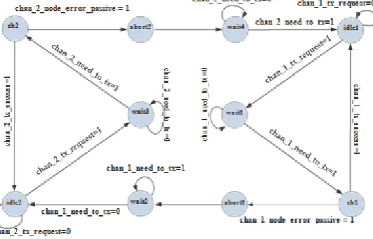
B. Redundancy management state-machine
International organization of Scientific Research 52 | P a g e
IV.
DRCC SIMULATION TEST
Among these tests, the DRCC IP core [13] is used as a component as if it was a chip in a Printed Circuit Board (PCB). Block diagram of the test system is shown in Fig.4. Task of the test program includes computing the expected timing of DRCC interface, writing read/write function and writing test bench [15, 16].
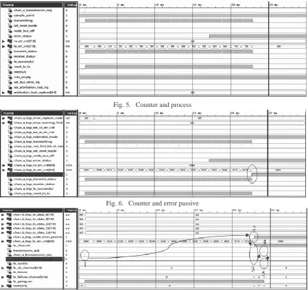
A. Transmission error count and transmission process
Simulation results of the relationship between transmission error count and transmission process are shown in Fig.5.
As shown in Fig.5, while transmitting signal is HIGH, a message is in the process of transmission. The signal bus of tx_err_cnt[7:0] is a indicator of transmission error counter, which will increase by 8 per transmission failure. While transmission error counter is more than 80Hex, the transmitting message of Channel1 is aborted.
B. Transmission error count and error passive activation
The results of simulation of a relationship between transmission error count and error passive activation is shown in Fig.6.
While transmission error counter (chan_a_bsp_tx_err_cnt[8:0]) is greater than 80Hex, the signal of ERROR PASSIVE (chan_a_bsp_node_error_passive) is activated. In redundancy mode, the state-machine will start the process of switching channel.
C. Switching channels
The results of simulation of switching channels are shown in Fig.7. 1) Step 1:
Fig. 5. Counter and process
Fig. 6. Counter and error passive
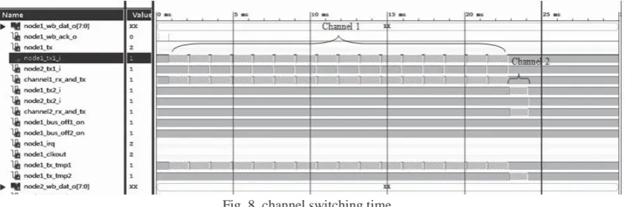
International organization of Scientific Research 54 | P a g e Fig. 8. channel switching time
4) Step 3:
In this phase, switching channel and request for transmitting the message from Channel 2 are done. When the machine sets tx_channel to HIGH, current channel has been connected to Channel 2. When the state-machine sets chan_b_transmission_req to HIGH, it requests to transmit the message from Channel 2.
5) Step 4:
signal of transmission_ack. When the message is successfully transmitted, the state-machine sets the signal to a clock period.
6) Step 5:
signal of tx_sucess. When the message is successfully transmitted, the state-machine sets the signal to a clock period.
D. Channel switching time
As shown in Fig.8, during 25ms or so, Channel 1 (node1_tx1_i) transmitted repeatedly a message but did not success. This leaded to ERROR PASSIVE activation and then the same message is switched to Channel 2 to transmit. Channel 2 (node1_tx2_i) completes successfully transmission only once. So, Channel switching time needs 25ms or so under the acknowledge error circumstance.
V.
CONCLUSIONS
The DRCC IP Core, which is written by synthesizable, behavioral Verilog language, can be used as a component in a project and it must have had a bright prospect for the future. By downloading the IP Core into a XILINX’s SPARTAN-3 chip [11] to test, the design of Dual Redundancy CAN-bus Controller Based on FPGA is successful. It guarantees reliability and real-time performance and compensates for the disadvantage of software redundancy.
VI.
ACKNOWLEDGMENT
We would like to give thanks to Professor Min Zijian for his help in the test and analysis of the IP Core.
REFERENCES
[1] Ma Xiaojun, Tong Jiarong, “Design and Implementation of A New FPGA Architecture,” ASIC, 20 03. Proceedings. 5th International Conference, Vol.2, pp.816-819, October 2003.
[2] Yu Zhu, Can and FPGA Communication Engineering: Implementation of a Can Bus Based Measurement System on an Fpga Development Kit, Diplomica Verlag, 2010.
[3] Philips Semiconductors. SJA1000 Standalone CAN controller. January 2000. [4] Qing Jia, DeviceNet media redundancy㧘iCC 2005.
[5] Robert Bosch GmbH, CAN Specification Version 2.0, September 1991.
[6] Jos´e Rufino, Dual-Media Redundancy Mechanisms for CAN, Technical Report, January 1997. [7] CiA - CAN in Automation. CAN Physical Layer for Industrial Applications - CiA/DS102-
Time Programming, Shantou, China, June 1998. IFAC/IFIP.
[14] Lattice Semiconductor Corporation, A Verilog HDL Test Bench Primer: Application Note. [15] Abhishek Shetty, Hamid Mahmoodi, System Verilog Testbench Tutorial,
Nano-Electronics & Computing Research Center School of Engineering San Francisco State University S an Francisco, C'A Fall 2011.
[16] S. Punnekkat, H. Hansson, and C. Norstrom, “Response time analysis under errors for CAN”, Proceedings of the IEEE Real-Time Technology and Applications Symposium, pp. 258-265, Washington, USA, May 2000.
[17] Robert I. Davis, Alan Burns, Controller Area Network (CAN) Schedulability Analysis.