Non-Destructive Defect Detection for MEMS Devices Using Transient Thermography
XIAOTING WANG, DAVID C. WHALLEY & V ADIM V. SILBERSCHMIDTWolfson School of Mechanical and Manufacturing Engineering, Loughborough University Loughborough, Leicestershire, LEI I 3TU, UK
Email: [email protected]@[email protected] Abstract
This paper investigates the use of transient infrared thermography in a transmission mode for subsurface defect detection within thin multilayer structures such as those found in MEMS devices. This was undertaken through the use of finite element analysis based simulations for several sizes of defects and for several combinations of substrate and thin film materials. The maximum temperature difference observable at the sample surface between defective and non-defective regions of the sample was investigated as a function of various parameters of the sample materials and defect geometry.
Introduction
In Micro-Electro-Mechanical Systems (MEMS) devices, such as pressure sensors and accelerometers, multilayer structures are widely used [1]. In contrast to monolithic engineering structures, such multilayer structures are made of more than one material, with the materials for the individual layers selected to meet specific functional requirements within the device. However, multiple layers within the device mean multiple material interfaces, which are often the location of defects, and require multiple manufacturing process steps which may increase the probability of defects occurring both during these fabrication processes and subsequently during device operation in service. This is because the interfaces between a thin film and a substrate, or between films, are critical to the integrity of these composite structures [2]. For example, defects such as delamination, cracking and void formation in devices can be induced by a mismatch between the thermal expansion coefficients (CTEs) of the different materials.
Two common analysis tools used for locating and evaluating defects in MEMS devices are optical and electron microscopes. For such analysis the sample typically must be cross-sectioned and then finely polished to obtain internal defect information, which is therefore a form of destructive testing. Considering the high cost and large number of test samples typically consumed during a programme of testing, non-destructive detection techniques (NDT) may be preferred and may also be used for quality control within the manufacturing process by monitoring the occurrence of defects in real time during inspection or burn-in tests. NDT methods may reduce the risk of defects not being identified at an early stage and therefore improve the finished product yield and quality.
NDT methods include technologies such as ultrasonic detection (acoustic microscopy), radiographic detection (e.g. microfocal X-ray), eddy current testing, magnetic techniques, thermography, etc. [3]. Ultrasound has been
commonly used in non-destructive detection by using measurements of the scattering or reflection of ultrasound from any interface that separates regions of differing acoustic impedance [4]. However, for complex objects, such as multilayer structures, the multiple reflections at the interfaces can result in an ultrasonic signature that is difficult to evaluate [5]. X-rays and gamma-rays are used in radiographic NDT as these types of short wavelength electromagnetic radiation are able to penetrate solid media while being partially absorbed. Radiographic methods can achieve high resolution and high quality detection of defects, such as voids or inclusions within the individual sample materials [6]. However, cracks and delamination are more difficult to detect and for multilayer and multiple-material samples, detection of defects will be made more difficult because of the typically large differences in absorption between different layers. Other NDT methods, such as eddy current testing and magnetic techniques, require specific sample materials (ferromagnetic and electrically conductive materials respectively) [7, 8]. In comparison, infrared thermography based detection can potentially be applied to the detection of internal cracks, voids and interface delamination within multilayer structures and for a wide range of metallic and non-metallic materials [9].
Infrared thermography is a method for non-contact measurement of the temperature distribution over the surface of an object through measurement of its thermal radiation. The working principle of infrared thermography as a NDT method is based on the difference in heat transfer characteristics between a continuous solid material and a defective region, such as a void, an inclusion of foreign material, a crack, or an area of delamination/disbonding between layers. Transient thermography is the most commonly used thermographic NDT technique and has been widely employed for the high resolution and non-destructive detection of defects [10]. It facilitates better defect detection than ordinary thermography, because it can achieve a larger surface temperature difference for a lower temperature increment and over a shorter time. Given the application of an appropriate thermal stimulus these differences in heat transfer will lead to differences in surface temperature between any feature(s) of interest and the remainder of the component. Thermographic measurement of these differences can therefore be used for detecting the defect [11]. This NDT method benefits from several advantages, for example being non-contact, high speed and requiring no use of harmful radiation. The concept of transient thermography was pioneered by Milne and Reynolds in 1981 [12], who called it pulsed video thermography. However, due to the limitations of thermal camera
Non-Destructive Defect Detection for MEMS Devices Using Transient Thermography
XIAOTING WANG, DAVID C. WHALLEY & V ADIM V. SILBERSCHMIDT Wolfson School of Mechanical and Manufacturing Engineering, Loughborough University
Loughborough, Leicestershire, LEI I 3TU, UK
Email: [email protected]@[email protected] Abstract
This paper investigates the use of transient infrared thermography in a transmission mode for subsurface defect detection within thin multilayer structures such as those found in MEMS devices. This was undertaken through the use of finite element analysis based simulations for several sizes of defects and for several combinations of substrate and thin film materials. The maximum temperature difference observable at the sample surface between defective and non-defective regions of the sample was investigated as a function of various parameters of the sample materials and defect geometry.
Introduction
In Micro-Electro-Mechanical Systems (MEMS) devices, such as pressure sensors and accelerometers, multilayer structures are widely used [1]. In contrast to monolithic engineering structures, such multilayer structures are made of more than one material, with the materials for the individual layers selected to meet specific functional requirements within the device. However, multiple layers within the device mean multiple material interfaces, which are often the location of defects, and require multiple manufacturing process steps which may increase the probability of defects occurring both during these fabrication processes and subsequently during device operation in service. This is because the interfaces between a thin film and a substrate, or between films, are critical to the integrity of these composite structures [2]. For example, defects such as delamination, cracking and void formation in devices can be induced by a mismatch between the thermal expansion coefficients (CTEs) of the different materials.
Two common analysis tools used for locating and evaluating defects in MEMS devices are optical and electron microscopes. For such analysis the sample typically must be cross-sectioned and then finely polished to obtain internal defect information, which is therefore a form of destructive testing. Considering the high cost and large number of test samples typically consumed during a programme of testing, non-destructive detection techniques (NDT) may be preferred and may also be used for quality control within the manufacturing process by monitoring the occurrence of defects in real time during inspection or burn-in tests. NDT methods may reduce the risk of defects not being identified at an early stage and therefore improve the finished product yield and quality.
NDT methods include technologies such as ultrasonic detection (acoustic microscopy), radiographic detection (e.g. microfocal X-ray), eddy current testing, magnetic techniques, thermography, etc. [3]. Ultrasound has been
commonly used in non-destructive detection by using measurements of the scattering or reflection of ultrasound from any interface that separates regions of differing acoustic impedance [4]. However, for complex objects, such as multilayer structures, the multiple reflections at the interfaces can result in an ultrasonic signature that is difficult to evaluate [5]. X-rays and gamma-rays are used in radiographic NDT as these types of short wavelength electromagnetic radiation are able to penetrate solid media while being partially absorbed. Radiographic methods can achieve high resolution and high quality detection of defects, such as voids or inclusions within the individual sample materials [6]. However, cracks and delamination are more difficult to detect and for multilayer and multiple-material samples, detection of defects will be made more difficult because of the typically large differences in absorption between different layers. Other NDT methods, such as eddy current testing and magnetic techniques, require specific sample materials (ferromagnetic and electrically conductive materials respectively) [7, 8]. In comparison, infrared thermography based detection can potentially be applied to the detection of internal cracks, voids and interface delamination within multilayer structures and for a wide range of metallic and non-metallic materials [9].
Infrared thermography is a method for non-contact measurement of the temperature distribution over the surface of an object through measurement of its thermal radiation. The working principle of infrared thermography as a NDT method is based on the difference in heat transfer characteristics between a continuous solid material and a defective region, such as a void, an inclusion of foreign material, a crack, or an area of delamination/disbonding between layers. Transient thermography is the most commonly used thermographic NDT technique and has been widely employed for the high resolution and non-destructive detection of defects [10]. It facilitates better defect detection than ordinary thermography, because it can achieve a larger surface temperature difference for a lower temperature increment and over a shorter time. Given the application of an appropriate thermal stimulus these differences in heat transfer will lead to differences in surface temperature between any feature(s) of interest and the remainder of the component. Thermographic measurement of these differences can therefore be used for detecting the defect [11]. This NDT method benefits from several advantages, for example being non-contact, high speed and requiring no use of harmful radiation. The concept of transient thermography was pioneered by Milne and Reynolds in 1981 [12], who called it pulsed video thermography. However, due to the limitations of thermal camera
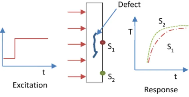
technology at that time, transient thermography didn't become popular until the 1990s. A major advantage of IR thermography for NDT is the detection and monitoring of sub-surface defects [13]. In the military, industrial and civil engineering fields, the most commonly used thermography based NDT method uses active "reflection" thermography [14], in which an external thermal stimulus is applied on the same side of the object of interest as the thermal camera. This approach removes the requirement to access the sample from both sides, but is also typically used because the substrate under the types of defect being sought tends to be relatively thick. In these applications the substrate under the defect can often be considered to be effectively infinitely thick and can therefore rapidly absorb most of the thermal excitation energy without any significant increase in temperature. Therefore, the thickness of the substrate has little effect and has typically not been considered in previous work [15]. When a subject is heated on the surface, thermal energy will conduct from the surface into the structure because of the temperature gradient. However, when the heat reaches a defect it will be obstructed from penetrating further into the substrate. The temperature over the defect will therefore rise faster than for sound areas. However, considering the size of typical MEMS devices and the short focal length (10-20 mm) of the thermal camera lenses that are necessary to achieve sufficient spatial resolution, transmission mode thermography, as shown in Figure 1, is more practical. Moreover, typical substrates used for MEMS devices are thin enough (100-1000 11m) to allow the thermal excitation to penetrate the sample quickly. Thus transmission mode infrared thermography is considered more suitable for MEMS defect detection.
Thermal excitation
Figure I Schematic of active thermographic NDT used in the transmission mode
In transmission mode thermography a defect will obstruct the flow of heat through the sample and there will therefore be a lower temperature area at the surface facing the thermal camera. However, because MEMS devices are very small, the object will quickly reach a uniform temperature unless the excitation is maintained and achieving a sufficient temperature difference between sound and defective areas for long enough to detect without causing thermal damage to the sample (overheating) is a key problem. As shown in Figure 2, the surface of the subject being tested is subjected to a sudden change in thermal conditions, either a step change in heat flux or temperature or a pulse of energy, which can be deployed by means of optical devices such as a flash lamp
or laser beam, or mechanically (e.g. using a sonic or ultrasonic transducer) [13]. The surface over a defective area will reach a different temperature after some period of time compared with undamaged areas [16]. Microelectronic applications of transient thermography have included detection of manufacturing defects in electronic circuit board assemblies [17] and it was more recently evaluated for the detection of electrical defects, such as short circuits and high resistance connections in microelectronic and micro system devices. The latter was achieved by applying a periodic voltage to the circuit, and its capability in locating the depth of point defects was demonstrated, although it was less successful for measurement of the size of 2D defects such as delamination and cracking [18, 19]. The application of transient thermography to the thin multilayer structures of MEMS devices has so far been extremely limited
Defect
be.
5 ,..} ::;:-:=.-.-_. ,l ,/ T/./
//
\
:I t t Excitation ResponseFigure 2 Schematic of transmission transient thermography
In this research, active transient thermography stimulated by an external thermal excitation was evaluated in terms of its ability to locate and measure the size of defects in multilayer structures comprised of two materials having different thermal properties. This was accomplished through the use of finite element method (FEM) models to predict the dynamic temperature distribution within these multilayer structures where they contain a defect.
Finite Element Modelling of Transmission Mode Transient Thermography
According to Fourier's law, when a temperature gradient exists within a body of uniform cross sectional area (A), the energy (q) transferred from the high-temperature to the low-high-temperature region is [20]:
aT
q
=
-kA ax (I)where k is the material thermal conductivity and aT/ax is the temperature gradient in the direction of the heat flow.
For constant material properties, the differential equation for the temperature distribution over a surface is:
a
2T
1aT
az2 a aT (2)
where the quantity a=k/pc is the thermal diffusivity of the material (a measure of how fast heat will diffuse through technology at that time, transient thermography didn't
become popular until the 1990s. A major advantage of IR thermography for NDT is the detection and monitoring of sub-surface defects [13]. In the military, industrial and civil engineering fields, the most commonly used thermography based NDT method uses active "reflection" thermography [14], in which an external thermal stimulus is applied on the same side of the object of interest as the thermal camera. This approach removes the requirement to access the sample from both sides, but is also typically used because the substrate under the types of defect being sought tends to be relatively thick. In these applications the substrate under the defect can often be considered to be effectively infinitely thick and can therefore rapidly absorb most of the thermal excitation energy without any significant increase in temperature. Therefore, the thickness of the substrate has little effect and has typically not been considered in previous work [15]. When a subject is heated on the surface, thermal energy will conduct from the surface into the structure because of the temperature gradient. However, when the heat reaches a defect it will be obstructed from penetrating further into the substrate. The temperature over the defect will therefore rise faster than for sound areas. However, considering the size of typical MEMS devices and the short focal length (10-20 mm) of the thermal camera lenses that are necessary to achieve sufficient spatial resolution, transmission mode thermography, as shown in Figure 1, is more practical. Moreover, typical substrates used for MEMS devices are thin enough (100-1000 11m) to allow the thermal excitation to penetrate the sample quickly. Thus transmission mode infrared thermography is considered more suitable for MEMS defect detection.
Thermal excitation
Figure I Schematic of active thermographic NDT used in the transmission mode
In transmission mode thermography a defect will obstruct the flow of heat through the sample and there will therefore be a lower temperature area at the surface facing the thermal camera. However, because MEMS devices are very small, the object will quickly reach a uniform temperature unless the excitation is maintained and achieving a sufficient temperature difference between sound and defective areas for long enough to detect without causing thermal damage to the sample (overheating) is a key problem. As shown in Figure 2, the surface of the subject being tested is subjected to a sudden change in thermal conditions, either a step change in heat flux or temperature or a pulse of energy, which can be deployed by means of optical devices such as a flash lamp
or laser beam, or mechanically (e.g. using a sonic or ultrasonic transducer) [13]. The surface over a defective area will reach a different temperature after some period of time compared with undamaged areas [16]. Microelectronic applications of transient thermography have included detection of manufacturing defects in electronic circuit board assemblies [17] and it was more recently evaluated for the detection of electrical defects, such as short circuits and high resistance connections in microelectronic and micro system devices. The latter was achieved by applying a periodic voltage to the circuit, and its capability in locating the depth of point defects was demonstrated, although it was less successful for measurement of the size of 2D defects such as delamination and cracking [18, 19]. The application of transient thermography to the thin multilayer structures of MEMS devices has so far been extremely limited
Defect
be.
5 ,..} ::;:-:=.-.-_. ,l ,/ T/./
//
\
:I t t Excitation ResponseFigure 2 Schematic of transmission transient thermography
In this research, active transient thermography stimulated by an external thermal excitation was evaluated in terms of its ability to locate and measure the size of defects in multilayer structures comprised of two materials having different thermal properties. This was accomplished through the use of finite element method (FEM) models to predict the dynamic temperature distribution within these multilayer structures where they contain a defect.
Finite Element Modelling of Transmission Mode Transient Thermography
According to Fourier's law, when a temperature gradient exists within a body of uniform cross sectional area (A), the energy (q) transferred from the high-temperature to the low-high-temperature region is [20]:
aT
q
=
-kA ax (I)where k is the material thermal conductivity and aT/ax is the temperature gradient in the direction of the heat flow.
For constant material properties, the differential equation for the temperature distribution over a surface is:
a
2T
1aT
az2 a aT (2)
where the quantity a=k/pc is the thermal diffusivity of the material (a measure of how fast heat will diffuse through
it i.e. the larger the value of (1., the faster heat will diffuse
through the material), p is its density, c is the specific heat capacity at constant pressure, and T is time.
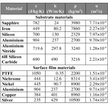
In order to simulate the thermographic inspection of some typical multilayer structures, a 2D axisymmetric heat transfer model has been developed using the commercial finite element modelling software COMSOL 5.0. The geometry of the model containing a defect is shown in Figure 3, while the geometric parameters are shown in Table 1. The overall radius of the model is 5 times the thickness of the substrate, which is sufficient for the model response to approximate that of an infinite plate. The mesh consisted of 5700 linear quadrilateral elements. Six substrate materials and six film materials which are commonly used in MEMS devices were used in the model. The relevant thermal properties of these materials are shown in Table 2 [20],
z ..
o
Radiation Convection It
J
Surface film Defect1===:::::1-- - - --1
Interface Substratei
External stimulation Figure 3 Schematic of the 2D axisymmetric model Table 1 Geometrical parameters of the two layer modelcontaining a defect
Geometrical parameter Values [/lm]
Radius of defect 20,40,50,60,80,100
Thickness of film 1,5,10,15,20
Thickness of defect 1
Thickness of substrate 50,100,150,200 Radius of film and substrate 1000
The initial temperature (i.e. when T
=
0) of the wholemodel, T(z, r, 0), is assigned the ambient temperature, Text I.e:
T(z, T, 0)
=
Text=
293 (3)The boundary condition applied on the bottom surface of the model is a sudden increase (step change) in temperature of lJ"T. The temperature of the lower surface of the substrate (Thouom) is therefore:
Tbottom(r> 0)
=
Text+
lJ"T (4)The temperature increments applied were 20, 50, 80 and 110°C. Because the thermal resistance of the defect is very much higher than the sound interface areas, the surfaces of the defect were treated as adiabatic, which means that any radiative or convective heat transfer between the surfaces of the defect is neglected. This means that the defect acts as a complete obstruction to
heat flow into the area of film above it. The surface boundary condition included radiation and convection, however it was found to contribute only a very small proportion of the heat transfer and can therefore be neglected. The convection heat transfer coefficient of 10 W/m2• K with respect to Text is applied to the top surface of the model, which is intended to represent heat transfer under typical ambient conditions [21].
Table 2 Thermal characteristics of typical materials utilised in MEMS [20]
...
...
...
~15
. ..,.
fPB>o ICIDfm)
I rlllJ ~ .1Il l la).Yl11A '~I
wsgmm
Substrate materials Sapphire 782 24 3980 7.71xlO·6 Iron 449 80.2 7860 2.27xlO·5 Silicon 700 130 2329 7.97x10⁵ Aluminium 904 237 2700 9.70x10 5 Aluminium 719.6 297.8 3240 1.28xl0 4 Nitride 6H Silicon 690 490 3216 2.21x10⁴ Carbide
Surface film materials
PTFE 1050 0.35 2200 1.51x10⁷ Nichrome 444 12.6 8314 3.41 x10 6 Nickel 445 90.7 8900 2.29x10 5 Aluminium 904 237 2700 9.71x10⁵ Copper 384 401 8960 1.16x10 4 Silver 235 429 10500 1.74 x 10 4
Results and Discussion
Max temperature difference and peak time
The finite element analyses were used to predict the temperature distribution 1000 I1S after the step change in boundary temperature. To evaluate the changing temperature distribution, three points on the top surface of the model were selected: above the defect centre, Tdc, at the edge of the defect, 7;1e, and in the sound area far away from the defect, Ts. Figure 4 shows these temperatures for the model of a 50 11m radius defect between a 20 11m thick Ni film and 200 11m thick Si substrate and with a lJ"T of 50°C. It can be seen that the three surface temperatures began to increase rapidly about 50 I1S after the bottom temperature changed and then the rate of change of temperature gradually reduces. The temperature difference, TdifJ; between Tdc and T, also rises very quickly, but achieves a peak value before declining more slowly. The time (170 I1s) when this maximum temperature difference occurs is referred to as the peak time. Figure 5 (a) shows the predicted surface temperature distribution at this peak time of 170 I1S. The black circle shows the defect edge location. A lower temperature area can be clearly seen within the circle, revealing the defect area. The Tdiff in this case is around 4 0C. Figure 5 (b) shows the temperature distribution throughout the cross-section of the model. For otherwise identical models, the maXImum temperature difference shows a linear it i.e. the larger the value of (1., the faster heat will diffuse
through the material), p is its density, c is the specific heat capacity at constant pressure, and T is time.
In order to simulate the thermographic inspection of some typical multilayer structures, a 2D axisymmetric heat transfer model has been developed using the commercial finite element modelling software COMSOL 5.0. The geometry of the model containing a defect is shown in Figure 3, while the geometric parameters are shown in Table 1. The overall radius of the model is 5 times the thickness of the substrate, which is sufficient for the model response to approximate that of an infinite plate. The mesh consisted of 5700 linear quadrilateral elements. Six substrate materials and six film materials which are commonly used in MEMS devices were used in the model. The relevant thermal properties of these materials are shown in Table 2 [20],
z ..
o
Radiation Convection It
J
Surface film Defect1===:::::1-- - - --1
Interface Substratei
External stimulation Figure 3 Schematic of the 2D axisymmetric model Table 1 Geometrical parameters of the two layer modelcontaining a defect
Geometrical parameter Values [/lm]
Radius of defect 20,40,50,60,80,100
Thickness of film 1,5,10,15,20
Thickness of defect 1
Thickness of substrate 50,100,150,200 Radius of film and substrate 1000
The initial temperature (i.e. when T
=
0) of the wholemodel, T(z, r, 0), is assigned the ambient temperature, Text I.e:
T(z, T, 0)
=
Text=
293 (3)The boundary condition applied on the bottom surface of the model is a sudden increase (step change) in temperature of lJ"T. The temperature of the lower surface of the substrate (Thouom) is therefore:
Tbottom(r> 0)
=
Text+
lJ"T (4)The temperature increments applied were 20, 50, 80 and 110°C. Because the thermal resistance of the defect is very much higher than the sound interface areas, the surfaces of the defect were treated as adiabatic, which means that any radiative or convective heat transfer between the surfaces of the defect is neglected. This means that the defect acts as a complete obstruction to
heat flow into the area of film above it. The surface boundary condition included radiation and convection, however it was found to contribute only a very small proportion of the heat transfer and can therefore be neglected. The convection heat transfer coefficient of 10 W/m2• K with respect to Text is applied to the top surface of the model, which is intended to represent heat transfer under typical ambient conditions [21].
Table 2 Thermal characteristics of typical materials utilised in MEMS [20]
...
...
...
~15
. ..,.
fPB>o ICIDfm)
I rlllJ ~ .1Il l la).Yl11A '~I
wsgmm
Substrate materials Sapphire 782 24 3980 7.71xlO·6 Iron 449 80.2 7860 2.27xlO·5 Silicon 700 130 2329 7.97x10⁵ Aluminium 904 237 2700 9.70x10 5 Aluminium 719.6 297.8 3240 1.28xl0 4 Nitride 6H Silicon 690 490 3216 2.21x10⁴ Carbide
Surface film materials
PTFE 1050 0.35 2200 1.51x10⁷ Nichrome 444 12.6 8314 3.41 x10 6 Nickel 445 90.7 8900 2.29x10 5 Aluminium 904 237 2700 9.71x10⁵ Copper 384 401 8960 1.16x10 4 Silver 235 429 10500 1.74 x 10 4
Results and Discussion
Max temperature difference and peak time
The finite element analyses were used to predict the temperature distribution 1000 I1S after the step change in boundary temperature. To evaluate the changing temperature distribution, three points on the top surface of the model were selected: above the defect centre, Tdc, at the edge of the defect, 7;1e, and in the sound area far away from the defect, Ts. Figure 4 shows these temperatures for the model of a 50 11m radius defect between a 20 11m thick Ni film and 200 11m thick Si substrate and with a lJ"T of 50°C. It can be seen that the three surface temperatures began to increase rapidly about 50 I1S after the bottom temperature changed and then the rate of change of temperature gradually reduces. The temperature difference, TdifJ; between Tdc and T, also rises very quickly, but achieves a peak value before declining more slowly. The time (170 I1s) when this maximum temperature difference occurs is referred to as the peak time. Figure 5 (a) shows the predicted surface temperature distribution at this peak time of 170 I1S. The black circle shows the defect edge location. A lower temperature area can be clearly seen within the circle, revealing the defect area. The Tdiff in this case is around 4 0C. Figure 5 (b) shows the temperature distribution throughout the cross-section of the model. For otherwise identical models, the maXImum temperature difference shows a linear
relationship with the temperature increment, while the peak times are the same, as shown in Figure 6. Thus, although increasing the heating temperature can achieve a larger temperature difference, the temperature of the whole specimen will also increase proportionally.
350 4 QJ :.. 340
=
3...
=
:.. QJ 330 ~ U Q.. 2~
::2'320 0 '-' E-'-' 1 ~ QJ 310 h"'" ~ ~ :.. 0 300 .... · .... Ts=
IJJ. - - - Ts-Tdc 290 -1 0 500 1000 Time (Ils)Figure 4 Surface temperatures (Tdc, T, and Tde) and surface
temperature-difference (Tdiff = T, -Tdc) between the defect
centre and non-damaged area versus time
(a) (b) 340 335 330 325 320 315 310 305
Figure 5 (a) Surface temperature image and (b) 2D slice image of the 50 [tm radius defect model after 170 Ils
The values of maximum temperature difference and peak time also have a relationship with the defect radius, film thickness, substrate thickness and the thermal properties of the substrate and film materials. As shown in Figure 7, which is otherwise for the same model as for the results in Figure 4, the temperature difference increases faster when the film is thinner and reaches a
higher peak value. However, the temperature difference and speed aren't proportional to the thickness. When the film is sufficiently thin, any through thickness temperature gradients have little effect. So, in this particular case, when the film thickness is less than about 5 11m, the max temperature difference does not change significantly. In contrast to the film thickness, varying the substrate thickness has the opposite effect, as shown in Figure 8. 10 8 ,.-., ~6 ~ h"'" 2 0 20 200 Time (Ils) - • - 20 C - - - 50 C ··· 80 C C 2000 Figure 6 Tdiff versus time for heating increments of 20, 40,
80 and 100°C 5 180 170 ,.-.,
...
U 160 o 4,5 ,.-., 'Ll '-' 150 =-!1; '-' h"'"'"
140""
'"
" io< 4'"
...
Co=
•
130::E
..
...
--+- maxTd -.-
time 120 3,5 110 0 5 10 15 20Thickness of film (Ilm)
Figure 7 Maximum temperature difference and peak time as a function of film thickness
20 U15 ~o l-x ro ~ 5 0 50 --+- MaxTd - . - peak time
...
..
',
100 150 200Thickness of substrate (Ilm)
200 150 "iii E; Q) 100.§
....
..lO: ro 50 ~o
Figure 8 Maximum temperature difference and peak time as a function of substrate thickness
Because the defect obstructs heat flow into the area of film above it, the distance heat must flow to the surface at the defect centre is proportional to its radius. Max TdijJ
therefore increases with the radius of defect and the time to Max Tdifris longer, as shown in Figure 9. Thus, a larger defect presents better detectability.
14 12 10 ,.-.,
~8
!1;6 E-o,'" 4 2 0 - - 20 llm - • - 40llm ---60llm ••••••••• 80llm 20 200 Time (Ils) 2000Figure 9 Temperature difference versus time for various defect radii
The thermal diffusivity of the film material also has a significant effect and, as shown in Figure 10 (a) and (b), film materials with a high thermal diffusivity present a smaller temperature difference and shorter peak time, which both reduce detectability. In contrast, lower thermal diffusivity provides better detectability as a result of the larger temperature difference and later peak time. The temperature distribution within a semi-infinite solid being heated through the surface to Tbottom has the
following relationship with thermal diffusivity and heating time [20]:
T(x, t) - Tbottom x
- - - =
erf(--)Text - Tbottom 2-J(ii (5)
where x is the distance from the bottom surface. When
~ is much smaller than 1, the error function, err, is
~~ .
approximately linear. The maximum temperature difference would therefore be expected to show an approximately linear relationship with
1/
-J
atpeak andFigure 10 (b) shows the maximum temperature difference plotted against 1/
-J
atpeak confirming this relationship.For the data presented in Figure 4, the time that the temperature difference exceeds l/e i.e. 63% of its peak value (2.36 0c) is 270 IlS. This demonstrates that this type of defect should be detectable with currently available high performance thermal cameras, such as the FUR Systems x8400sc, which can operate with integration times as short as 500 ns and provides a minimum pixel pitch, using a close up lens, of 5 11m. It should therefore be possible for such a high speed thermal camera to acquire the surface temperature distribution over a defect in a NilSi structure. However, as shown in Figure 10 for high diffusivity film materials such as AI, Cu, Ag, etc., the max Tdifrfor a 50 11m defect is smaller than 0.7 °C and the observation periods are around 200 I1S. For such materials with micro size defects, the possibility of detection will be smaller than that for lower thermal diffusivity film materials such as Nichrome and PTFE.
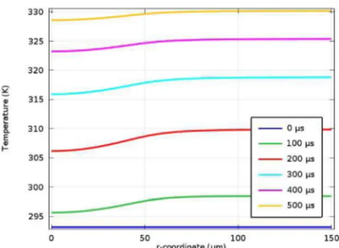
Temperature gradient
Figure 12 shows the surface temperature profiles from the defect centre to the edge of the model at 0, 100, 200, 300, 400, and 500 I1S after commencing heating. These predicted temperatures indicate a significantly lower temperature area above the defect during heating. The surface temperature over the defect centre (Tdc) is the lowest, and rises with the radius. Meanwhile, the average temperature of the specimen rises sharply with time .
3,00 •• PTFE 2,50 ,.-.,
E
2,00 "-' ~ E 1,50 -.;::: -" ~ 1,00 Q. 0,50 0,00 (a) 40 35 30 ,.-.,~
25 "-'E-o,~20
io< 15 <:':I::E
10 5 0 (b) 0 ~ •• j'J iCr AI ~ · -Noi···."..
~.
.c;:u ••••••• ;::K Ago
0,00005 0,0001 0,00015 0,0002 a (m2/s) Cu •••••• Ni Ag_~ /-\1 20t
PTFE ••• NiCr 40 60Figure 10 (a) Peak time and (b) Maximum temperature difference vs. thermal diffusivity for various film
materials 12 10
••••
SiC.
,.-.,.
U 8. .
0.
"-'.
!1; 6 ~" AIN E-o,'" io<» ..
;L\I <:':I::E
4. ·· Si
.
.
2.·~e
0 ~" AIOo
0,0001 0,0002 0,0003 a (m2/s)Figure II Max temperature difference vs. thermal diffusivity of substrate material
therefore increases with the radius of defect and the time to Max Tdifris longer, as shown in Figure 9. Thus, a larger defect presents better detectability.
14 12 10 ,.-.,
~8
!1;6 E-o,'" 4 2 0 - - 20 llm - • - 40llm ---60llm ••••••••• 80llm 20 200 Time (Ils) 2000Figure 9 Temperature difference versus time for various defect radii
The thermal diffusivity of the film material also has a significant effect and, as shown in Figure 10 (a) and (b), film materials with a high thermal diffusivity present a smaller temperature difference and shorter peak time, which both reduce detectability. In contrast, lower thermal diffusivity provides better detectability as a result of the larger temperature difference and later peak time. The temperature distribution within a semi-infinite solid being heated through the surface to Tbottom has the
following relationship with thermal diffusivity and heating time [20]:
T(x, t) - Tbottom x
- - - =
erf(--)Text - Tbottom 2-J(ii (5)
where x is the distance from the bottom surface. When
~ is much smaller than 1, the error function, err, is
~~ .
approximately linear. The maximum temperature difference would therefore be expected to show an approximately linear relationship with
1/
-J
atpeak andFigure 10 (b) shows the maximum temperature difference plotted against 1/
-J
atpeak confirming this relationship.For the data presented in Figure 4, the time that the temperature difference exceeds l/e i.e. 63% of its peak value (2.36 0c) is 270 IlS. This demonstrates that this type of defect should be detectable with currently available high performance thermal cameras, such as the FUR Systems x8400sc, which can operate with integration times as short as 500 ns and provides a minimum pixel pitch, using a close up lens, of 5 11m. It should therefore be possible for such a high speed thermal camera to acquire the surface temperature distribution over a defect in a NilSi structure. However, as shown in Figure 10 for high diffusivity film materials such as AI, Cu, Ag, etc., the max Tdifrfor a 50 11m defect is smaller than 0.7 °C and the observation periods are around 200 I1S. For such materials with micro size defects, the possibility of detection will be smaller than that for lower thermal diffusivity film materials such as Nichrome and PTFE.
Temperature gradient
Figure 12 shows the surface temperature profiles from the defect centre to the edge of the model at 0, 100, 200, 300, 400, and 500 I1S after commencing heating. These predicted temperatures indicate a significantly lower temperature area above the defect during heating. The surface temperature over the defect centre (Tdc) is the lowest, and rises with the radius. Meanwhile, the average temperature of the specimen rises sharply with time .
3,00 •• PTFE 2,50 ,.-.,
E
2,00 "-' ~ E 1,50 -.;::: -" ~ 1,00 Q. 0,50 0,00 (a) 40 35 30 ,.-.,~
25 "-'E-o,~20
io< 15 <:':I::E
10 5 0 (b) 0 ~ •• j'J iCr AI ~ · -Noi···."..
~.
.c;:u ••••••• ;::K Ago
0,00005 0,0001 0,00015 0,0002 a (m2/s) Cu •••••• Ni Ag_~ /-\1 20t
PTFE ••• NiCr 40 60Figure 10 (a) Peak time and (b) Maximum temperature difference vs. thermal diffusivity for various film
materials 12 10
••••
SiC.
,.-.,.
U 8. .
0.
"-'.
!1; 6 ~" AIN E-o,'" io<» ..
;L\I <:':I::E
4. ·· Si
.
.
2.·~e
0 ~" AIOo
0,0001 0,0002 0,0003 a (m2/s)Figure II Max temperature difference vs. thermal diffusivity of substrate material
330
-325 320 g ~ 31 5---~ 'i! ~ 310 E -- O~s r--- lOO~s ~ f-305 1- - -200~s - -300~s 30 0 - -400~s f-500 ~s 295 a 50 100 150
r~coord i nate 'I-'m )
Figure 12 Variation of the surface temperature with distance from the defect centre after different heating
times
Figure 13 shows the temperature gradient (dTldr) for the 50 11m defect model and shows that the location of the peak temperature gradient value can be used to provide a good estimate for the position of the defect edge. The analysis results also show that the maximum temperature gradient values vary with heating time, but that the radius of the peak value position is almost the same. This is different from the results in reflection mode obtained by Almond & Lau [22] where the measured defect radius was found to decrease with time.
E g ~ c w c a "-E 8 ~ ~. c w '0 E
'"
~ Z E w "-E w f-70000 60000 50000 40000 - - O f'S 30000 - - 100 ~s - - 200 ~s 20000 - - 300 ~s - - 400 ~s 10000 - - 500 ~s 0 0 20 40 60 80 100 120 140 Radia l dist a nce ( 11m )Figure 13 Surface temperature gradient versus radial position at different times
Conclusions
This study has explored the use of transmission mode transient thermography for the detection and measurement of subsurface defects in MEMS devices. The conclusions from the research can be summarised into several main components:
• Transient infrared thermography in transmission mode has the potential to provide non-destructive detection of internal defects in MEMS devices;
• The size of a defect can be estimated using the surface temperature gradient, whilst a larger defect provides better detectability;
• The maximal temperature difference increases almost linearly with the thermal diffusivity of the substrate material, but decreases in a more complex way with the thermal diffusivity of the film material;
• The maximal temperature difference occurs earlier if a higher thermal diffusivity material is used for the substrate;
• Lower thermal diffusivity film materials, such as PTFE, NiCr and Ni, can provide better detectability, in contrast with higher diffusivity films such as Ag, Cu and AI;
• The maximal temperature difference decreases with the thicknesses of both film and substrate, while the time to achieving this maximum becomes longer. Considering MEMS device film thicknesses, which are typically of the order of a few 11m, the substrate thickness has a more important effect on detectability;
• Transient thermography is suitable for the non-destructive detection for solar cell, MEMS and electronics devices, etc. Defects such as delamination and voids with a size down to a few hundred microns can be detected if the thermal camera with micro lens can offer microsecond between frames;
• The results indicate that the estimation of defect size will be more consistent for transmission mode thermography than for reflection mode.
References
1. Hsu, T. R. "Reliability in MEMS packaging", Proceedings of the 2006 IEEE International Reliability Physics Symposium, San Jose, CA, March 2006, pp. 398 - 402
2. Witvrouw, A., Tilmans, H. A. C. & De Wolf, I. "Materials issues in the processing, the operation and the reliability of MEMS", Microelectronic Engineering, Vol. 76, No. I (2004), pp. 245-257. 3. Scott, I. G. and Scala, C. M. "A review of
non-destructive testing of composite materials", NDT International, Vol. 15, No.2 (1982), pp. 75-86. 4. Wickramasinghe, H. K. "Scanning acoustic
microscopy: a review", Journal of Microscopy, Vol. 129,No.1 (l983),pp.63-73.
5. Bechou, L., Gusten, Y. and Danto, Y. "New methods for scanning ultrasonic microscopy applications for failure analysis of microassembling technologies", Proceedings of the 2001 8th International Symposium on the Physical and Failure Analysis of Integrated Circuits. Jun. 2001, pp. 195-201
6. Lin, C. L. & Miller, J. D. "Cone beam X-ray microtomography-a new facility for three-dimensional analysis of muItiphase materials", Minerals and Metallurgical Processing Vol. 19, No. 2 (2002), pp. 65-71.
7. Garda-Martin, J., Gomez-Gil, J. & Vazquez-Sanchez, E. "Non-destructive techniques based on eddy current testing", Sensors Vol. 11, No.3 (2011), pp. 2525-2565.
8. Jiles, D. C. "Review of magnetic methods for nondestructive evaluation (Part 2)", NDT
International, Vol. 23, No.2 (1990), pp. 83-92. 9. Roemer, J., Pieczonka, L., Szwedo, M,. Uhl, T. &
Staszewski, W. J. "Thermography of Metallic and Composite Structures-review of applications", International Workshop on Smart Materials, Structures & SHM, Calgary, Alberta, Jan. 2013. 10. Meola, C. & Carlomagno, G. M. "Recent advances in
the use of infrared thermography", Measurement science and technology, Vol. 15, No.9 (2004), pp. R27-R58.
11. Maldague, X. P, Nondestructive evaluation of materials by infrared thermography, Springer Science & Business Media (London, 2012)
12. Milne, J. M. and Reynolds. W. N. "The non-destructive evaluation of composites and other materials by thermal pulse video thermography", Thermosense VII: Thermal Infrared Sensing for Diagnostics and Control, Cambridge, Oct. 1985, pp. 119-122.
13. Kordatos, E. Z., Aggelis, D. G. & Matikas, T. E. "Monitoring mechanical damage in structural materials using complimentary NDE techniques based on thermography and acoustic emission", Composites Part B: Engineering, Vol. 43. No.6 (2012), pp. 2676-2686.
14. Maldague, X. P. "Introduction to NDT by active infrared thermography", Materials Evaluation, Vol. 60, No.9 (2002), pp. 1060-1073.
15. Connolly, M. P. "A review of factors influencing defect detection III infrared thermography:
applications to coated materials", Journal of nondestructive evaluation, Vol. 10, No.3 (1991), pp. 89-96.
16. McCann, D. M. & Forde, M. C. "Review of NDT methods in the assessment of concrete and masonry structures", NDT & E International, Vol. 34. No.2 (2001), pp. 71-84.
17. Hartless, P. C. M, & Whalley, D. C. "Automated thermographic inspection of surface mount solder joints", Eighth International Conference on Automotive Electronics, London, Oct. 1991, pp.
178-181.
18. Breitenstein, 0, Schmidt. C. & Karg. D. "Thermal failure analysis by IR lock-in thermography", Microelectronics Failure Analysis: Desk Reference, 5th edn. ASM International, Materials Park (2004), pp. 330-339.
19. Schmidt,
c.,
Altmann, F, Naumann, F, & Lindner, A. "Application of Lock-in-Thermography for 3d defect localisation in complex devices", Proceeding of the 2nd IEEE Electronics System-Integration Technology Conference, 2008.20. Bergman, T. L, Incropera, F. P, DeWitt, D. P, & Lavine, A. S. Fundamentals of heat and mass transfer, John Wiley & Sons, (2011).
21. Mehendale, S. S., Jacobi, A. M. & Shah, R. K. "Fluid flow and heat transfer at micro-and meso-scales with application to heat exchanger design", Applied Mechanics Reviews, Vol. 53. No.7 (2000), pp.
175-193.
22. Almond, D. P. & Lau, S. K. "Defect sizing by transient thermography. I. An analytical treatment", Journal of Physics D: Applied Physics, Vol. 27 No.5 (1994), pp. 1063-1069.