HIGH FREQUENCY AND HIGH DYNAMIC RANGE CONTINUOUS TIME FILTERS
A Dissertation by
ARTUR JULIUSZ LEWINSKI KOMINCZ
Submitted to the Office of Graduate Studies of Texas A&M University
in partial fulfillment of the requirements for the degree of DOCTOR OF PHILOSOPHY
May 2006
© 2006
ARTUR JULIUSZ LEWINSKI KOMINCZ
HIGH FREQUENCY AND HIGH DYNAMIC RANGE CONTINUOUS TIME FILTERS
A Dissertation by
ARTUR JULIUSZ LEWINSKI KOMINCZ
Submitted to the Office of Graduate Studies of Texas A&M University
in partial fulfillment of the requirements for the degree of DOCTOR OF PHILOSOPHY
Approved by:
Chair of Committee, Jose Silva Martinez Committee Members, Edgar Sanchez Sinencio
Frederick Strieter
Wayne Lepori
Head of Department, Costas Georghiades
May 2006
ABSTRACT
High Frequency and High Dynamic Range Continuous Time Filters. (May 2006)
Artur Juliusz Lewinski Komincz,
B.S., Instituto Tecnologico de Queretaro, Mexico Chair of Advisory Committee: Dr. Jose Silva Martinez
Many modern communication systems use orthogonal frequency division multiplexing (OFDM) and discrete multi-tone (DMT) as modulation schemes where high data rates are transmitted over a wide frequency band in multiple orthogonal sub-carriers. Due to the many advantages, such as flexibility, good noise immunity and the ability to be optimized for medium conditions, the use of DMT and OFDM can be found in digital video broadcasting, local area wireless network (IEEE 802.11a), asymmetric digital subscriber line (ADSL), very high bit rate DSL (VDSL) and power line communications (PLC). However, a major challenge is the design of the analog front-end; for these systems a large dynamic range is required due to the significant peak to average ratio of the resulting signals. In receivers, very demanding high-performance analog filters are typically used to block interferers and provide anti-aliasing before the subsequent analog to digital conversion stage.
For frequencies higher than 10MHz, Gm-C filter implementations are generally preferred due to the more efficient operation of wide-band operational transconductance amplifiers (OTA). Nevertheless, the inherent low-linearity of open-loop operated OTA limits the dynamic range. In this dissertation, three different proposed OTA linearity enhancement techniques for the design of high frequency and high dynamic range are presented. The techniques are applied to two filter implementations: a 20MHz second order tunable filter and a 30MHz fifth order elliptical low-pass filter. Simulation and experimental results show a spurious free dynamic range (SFDR) of 65dB with a power consumption of 85mW. In a figure of merit where SFDR is normalized to the power consumption, this filter is 6dB above the trend-line of recently reported continuous time filters.
To my wife Isabel, my parents Juliusz and Grazyna
ACKNOWLEDGMENTS
This work would not have been possible without the support and help of many people; my appreciation goes out to the following:
First, I would like to thank my advisor and committee chair, Dr. Jose Silva, for his outstanding guidance and knowledge during the course of this research. Also, thanks to all my committee members, Dr. Edgar Sanchez Sinencio, Dr. Frederick Strieter and Dr. Wayne Lepori for their great support and attention. It was an honor to work with all of them.
During the course of my Ph.D., the best thing happened to me: I married the love of my life, Isabel. Through good or hard times, she was always cheering me on and bringing joy to my life. There are no words to express my appreciation for that. I love her very much.
I want to give special thanks to Dr. Rainer Fink, for whom I had the opportunity to work in a remarkable and enjoyable project. Not only has he been a great supervisor and professor, but also a good friend who was always there to listen and advise.
Many thanks to my friends and former roommates David and Alberto; we shared together the glory and pain of graduate work, and we learned a lot from each other. To my friends Ari, Marcia, Pedro, Marta, Antonio and Adriana, thank you for your good advice, and for your kind help in times of need.
To Chinmaya, Faisal, Chava, Didem, Feyza, Sebastian, Peyman, Alexander, Hezam, Ranga, Rhadika, Alejandro, Wennie, Julio, Rida, Ahmed, Reza, Sathya, Taner,
Abraham, John, Lorena, Felipe, Gavillero, Pankaj, Sualp, Devrim, Fikret, Elvis, Itza; thanks for great shared moments.
I also want to thank my father for inspiring me to do this, and my mother for always believing in me. Thanks also to my wife’s parents for their constant support.
Many thanks go to Mrs. Cook, Nancy and Angela at Sponsored Student Services and Tammy, Jeannie and Ella at the Department of Electrical Engineering for their assistance.
Finally, I want to thank CONACYT for the invaluable financial support that made the achievement of this degree possible.
TABLE OF CONTENTS
Page
1. INTRODUCTION... 1
1.1 The need of analog filters... 1
1.2 Challenges in continuous-time filters... 5
1.3 State of the art in continuous time filters ... 10
1.4 Contributions ... 12
1.5 Organization ... 14
2. LINEARITY ENHANCEMENT TECHNIQUES BASED ON NON-LINEARITY CANCELLATION ... 15
2.1 The differential pair... 15
2.1.1 Distortion... 16
2.1.2 Noise... 23
2.2 The double differential pair... 26
2.2.1 Analysis ... 26
2.2.2 Improvement comparison... 31
2.3 A 20 MHz second order low-pass filter ... 35
2.3.1 OTA design ... 35
2.3.2 Filter design... 39
2.3.3 Experimental results ... 41
2.4 The triple differential pair ... 47
2.4.1 Analysis ... 47
2.4.2 Advantages of the topology... 52
2.4.3 Complete OTA ... 55
2.4.4 Experimental results ... 56
2.4.5 Comparison with reported OTAs ... 59
3. LINEARITY TECHNIQUES BASED ON NON-LINEAR SOURCE DEGENERATION ... 61
3.1 Non-linear degeneration principle... 61
3.2 A 30-MHz low-pass filter implementation ... 74
3.2.1 Design considerations ... 74
3.2.2 Filter structure. ... 78
3.2.3 Transconductors ... 80
3.2.4 Common mode feedback... 86
3.2.5 Self-bias circuit ... 87
3.2.6 Capacitors... 90
Page
3.3.1 Master circuit... 97
3.3.1 Analog section... 99
3.3.2 Digital tuning circuit ... 103
3.3.3 Non-idealities ... 104
3.3.3.1 Jitter and mismatch (offset)... 105
3.3.3.2 Output resistance ... 105 3.3.3.3 Parasitic capacitances ... 107 3.3.4 Overall accuracy... 108 3.4 Experimental results ... 110 3.4.1 Frequency response ... 112 3.4.2 Linearity ... 113
3.5. Comparison with state of the art solutions ... 118
4. CONCLUSION ... 121
REFERENCES... 123
LIST OF FIGURES
Page
Fig. 1.1 The use of filters to reduce the input range of an ADC. ... 2
Fig. 1.2. The use of filters to avoid the aliasing problem... 3
Fig. 1.3. Simplified schematic of a DSL modem. ... 4
Fig. 1.4. OFDM signal in a) frequency domain and b) time domain. ... 7
Fig. 1.5 Intermodulation components caused by the distortion of the filter. ... 8
Fig. 1.6 Figure of merit of recent publications about filters. ... 12
Fig. 2.1. The differential pair. ... 16
Fig. 2.2. Differential pair with tail current transistor. ... 19
Fig. 2.3. Differential pair with source degeneration... 20
Fig. 2.4. Noise sources in the degenerated differential pair. ... 23
Fig. 2.5. Pseudo-differential pair with the tail current in the middle. ... 25
Fig. 2.6. The double differential pair... 27
Fig. 2.7. Cadence IM3 simulations for the circuit of figure 2.6... 29
Fig. 2.8. Relation between IT1 and IT2 for optimal linearity. ... 30
Fig. 2.9. SDP and DDP designs for comparison with same transconductance, Vdsat and power consumption... 32
Fig. 2.10. Improvement in IM3 of the DDP over the SDP. ... 34
Fig. 2.11 IM3 plot vs. frequency. ... 35
Fig. 2.12 OTA design. ... 36
Fig. 2.13. Second order ladder low-pass prototype... 39
Fig. 2.14. Low-pass OTA implementation of the ladder filter... 40
Page
Fig. 2.16. Micrograph of the chip... 42
Fig. 2.17. IM3 of the filter and TOTA for several currents IT1 and IT2. ... 43
Fig. 2.18. Effect of the transconductance control over the IM3... 44
Fig. 2.19. IM3 measurement at 20Mhz, 1.3 Vpp input. ... 44
Fig. 2.20. Programmable frequency responses of the filter. ... 45
Fig. 2.21. Figure of merit of the filter in comparison with the state of the art in filters. ... 47
Fig. 2.22. The triple differential pair block diagram. ... 48
Fig. 2.23. (a) Degenerated DP, (b) degenerated DP with the tail current in the middle of the resistor and (c) proposed triple DP... 50
Fig. 2.24. Simulated and theoretical THD for circuits in fig. 2.23... 51
Fig. 2.25. Simulations of circuits in fig. 2.23 for different values of R. ... 53
Fig. 2.26. Complete OTA using complementary triple-DP. ... 55
Fig. 2.27. Micrograph of the OTA. ... 56
Fig. 2.28. Intermodulation test for a 1.3Vpp input at 20MHz... 58
Fig. 2.29. IM3 vs. frequency. ... 58
Fig. 3.1. Non-linear degeneration resistance DP concept. ... 62
Fig. 3.2. Implementation of the non-linear resistor using an auxiliary differential pair (ADP). ... 63
Fig. 3.3. (a) Transconductance plots for different sizes of MP. (b) Values ofGM1P and GM3P for different transistor sizes. ... 68
Fig. 3.4. Theoretical and practical IM3 for different Wp/Lp ratio. ... 69
Page Fig. 3.6. Scatter plot of Monte Carlo simulation of IM3 with and without ADP
including process parameter variations. It is shown that at least 10dB
improvement in IM3 can be guaranteed. ... 72
Fig. 3.7. A generic ladder low-pass filter. ... 75
Fig. 3.8. (a) Active inductance simulation using transconductors. (b) Noise representation of the active inductor... 76
Fig. 3.9. Noise model of a ladder low-pass filter at low frequencies. ... 77
Fig. 3.10. Ladder implementation of the elliptic filter 5h order. ... 79
Fig. 3.11. OTA-C implementation of the filter. ... 80
Fig. 3.12 OTA design. ... 81
Fig. 3.13. Micrograph of the OTA. ... 85
Fig. 3.14. Diagram of the OTA with the common mode feed-back... 86
Fig. 3.15. Auto-bias circuit concept. ... 88
Fig. 3.16. Comparator schematic. ... 89
Fig. 3.17 . IM3 vs. offset voltage in the comparator (Voff). ... 90
Fig. 3.18. Switched capacitor array for frequency tuning. Cnominal = 1.5*C. On grounded capacitors CB is connected to ground. ... 92
Fig. 3.19. Programmable AC responses in the filter. ... 94
Fig. 3.20. Master-slave approach. ... 95
Fig. 3.21. Automatic tuning (analog section)... 98
Fig. 3.22. Typical timing waveforms. ... 98
Fig. 3.23. Block diagram of the digital control loop. ... 99
Fig. 3.24. Transfer function changes with variations in individual capacitances. ... 100
Page
Fig. 3.26. Comparator used in the automatic tuning. ... 103
Fig. 3.27. Clock generator. ... 104
Fig. 3.28. Digital control section... 104
Fig. 3.29. Deviation of the ideal ramp due to the finite output resistance. ... 106
Fig. 3.30. Parasitic capacitances in an OTA pair. ... 108
Fig. 3.31. Variations of the magnitude response with and without automatic tuning. ... 109
Fig. 3.32 Variations of the magnitude response with automatic tuning and mismatches. ... 110
Fig. 3.33. Micrograph of the chip... 111
Fig. 3.34. Test set-up. ... 112
Fig. 3.35. Measured AC responses... 113
Fig. 3.36. Intermodulation tests at 20MHz... 114
Fig. 3.37. IM3 vs. frequency. ... 115
Fig. 3.38. Internal node AC response... 116
Fig. 3.39. Out of band IM3 test. ... 117
LIST OF TABLES
Page
Table 2.1. Results for the comparison between SDP and DDP. ... 33
Table 2.2. Transistor sizes for the OTA. Length for all transistors is 1µm. ... 38
Table 2.3. Summary of experimental results of the filter... 45
Table 2.4. Summary of experimental results... 57
Table 2.5. Comparison with recently reported OTAs. ... 60
Table 3.1 Approximation results. ... 78
Table 3.2. Transistor sizes... 84
Table 3.3. OTA: simulated parameters with R=500Ω. ... 84
Table 3.4. Nominal capacitor values. ... 92
1. INTRODUCTION
1.1 The need of analog filters
With low-power and small integrated circuits based on microprocessors, microcontrollers and digital signal processors (DSP), much of the electrical functionality previously implemented with analog electronics, is now efficiently done with digital circuits. This rapid grow in digital electronics deluded to a common misconception that electronic circuits known as “analog” are eventually going to disappear. However, in order to acquire and generate natural signals such as audio, video, radio waves and many others, the need of an analog to digital and digital to analog interfaces remains a must.
Before an analog signal enters the analog to digital converter (ADC), it must be preprocessed by analog continuous time filters (CTF) or a combination between continuous time filters (CTF) and switched capacitors. The CTF serves two main purposes: i) it rejects unwanted frequency signals to avoid overloading the ADC and ii) prevents aliasing by attenuating components with higher frequency components.
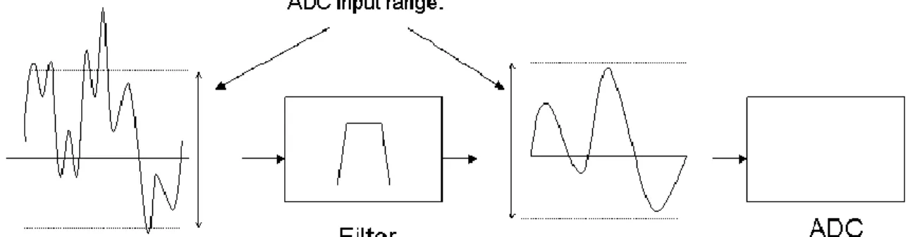
Figure 1.1 shows a typical signal in time domain where the amplitude is larger than the input range of the ADC marked with dashed lines. This signal may contain media noise, adjacent frequency channels not intended to be used by the end user, a DC signal, etc. A band-pass filter removes the undesired information, maintaining in-band information
intended for the application. An alternative to the use of analog filters is the removal of out of band signals using digital processing after the ADC, but a larger requirement in the number of bits would be necessary. For example, it has been shown in [1] that the additional necessary number of bits (N) of an ADC to accommodate out of band signals is: dB S I Int N 6 3 + = (1.1)
where I is the power (in dB) of the out of band signals and S is the power of the data to be captured. (Int stands for the integer function) Without the filter, an additional number of bits would complicate the ADC implementation.
Fig. 1.1 The use of filters to reduce the input range of an ADC.
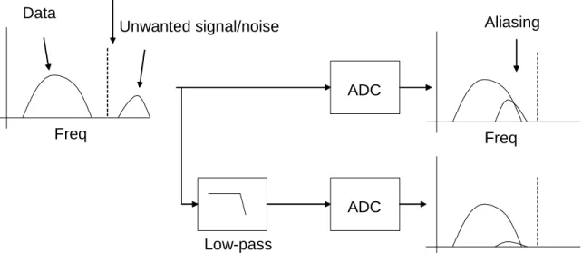
Whenever a continuous signal is sampled, all the frequencies above half the sampling rate are aliased back to the band of interest; this effect is known as aliasing . Figure 1.2 shows the frequency spectrum of a signal with higher frequency components higher than the half of the sampling rate of the ADC. Once the entire signal is sampled,
the undesired frequency components are aliased back into low frequency, tampering the useful data. To avoid this effect, a low-pass filter is necessary to remove higher frequency components.
Freq
ADC Sampling rate/2
Data Unwanted signal/noise Freq Aliasing Freq ADC ADC Low-pass (antialias) Filter.
Fig. 1.2. The use of filters to avoid the aliasing problem.
Although there is interest in developing powerful ADCs to remove analog filters and other analog blocks, technological limitations prevent this from being possible [2]. For low frequency operations, high resolutions can be achieved but as frequency increases higher power consumption designs are required to deal with parasitic capacitances that introduce bandwidth limitation; mismatch is also a limiting factor to the accuracy of an ADC. Digital to analog interfaces, also require continuous time
analog filters at the end of the signal path to smoothen the output generated by the digital to analog converter (DAC).
Figure 1.3 shows a block diagram of a typical modern communication system used in wired applications: a DSL modem. In the receive path, the incoming signal, which is weak due to attenuation in the cable, is amplified by a programmable gain amplifier (PGA1). A continuous time filter passes the required range of frequency spectrum while attenuating the out of band information and minimizing the alias signals for the subsequent analog to digital conversion. A second programmable gain amplifier (PGA2) may be used to further adjust the level of the signal to meet the input range of the analog to digital converter (ADC). The signal is then demodulated in the digital domain by the digital signal processor (DSP) and sent out to the user.
Cable PGA1 Filter 1 PGA2
1010 DSP ADC 1010 DAC Filter 2 Line Driver To computer Hybrid Receive path Transmit path
Fig. 1.3. Simplified schematic of a DSL modem.
In the transmit path, the digital data to be sent through the cable is modulated and converted to an analog signal by the use of a digital to analog converter (DAC). The
continuous time filter smoothes the pulse-shaped analog DAC output. Finally, a line driver sends the signal through the cable.
1.2 Challenges in continuous-time filters
The first filters that used resistors, inductors and capacitors are commonly known as RLC filters. These passive components occupied a very large area, especially at audio frequencies where heavy coils and big capacitors were the most noticeable components in the circuit board. Other applications, such as frequency division multiplexing telephone systems, required cheaper and smaller implementations. This gave rise to miniaturized piezoelectric technologies such as mechanical and crystal filters. Another similar technology based on acoustic waves, is the Surface Acoustic Wave (SAW) filter which is widely used in today’s wireless communication circuits. A detailed description of the previous mentioned filters can be found in [3].
Since the invention of the integrated circuit in 1958, more and more external circuitry was merged into a single chip and, as the resolution of integration increases, the concept of having an entire system on a chip (SoC) became possible. Circuit blocks such as the microcontroller, digital signal processor, analog to digital converters and filters can be now integrated into a single chip resulting in cost savings, space reduction and simple interface. Thanks to these features, it is possible to have affordable compact cell phones, miniaturized biomedical implants, portable computers and many other devices.
Although feasible, the integration of continuous time filters presents several problems. The integration of inductors in a small semiconductor die is not possible for frequencies lower than several hundreds for megahertz due to very large area requirements and the considerable resistivity of metal layers used to build an inductor. Therefore, active elements based on transistors have to be used to emulate inductors to implement equivalent transfer functions. Unfortunately, active elements introduce additional noise, harmonic distortion components and consume static power. Another problem is that integrated capacitors, resistors and active elements are sensitive to temperature and process parameters variations which affect the selectivity and precision of the filter.
The aforementioned disadvantages present a stringent challenge for many modern communication systems. Actually, integrated continuous time filters have been referred by some authors as “the bottleneck” of communication circuits [4]. This is especially the case of systems using orthogonal frequency division multiplexing (OFDM) and discrete multi-tone (DMT) as modulation schemes. In these schemes, high data rates are transmitted over a wide frequency band in multiple orthogonal sub-carriers. Due to its many advantages such as flexibility, good noise immunity and the ability to be optimized for medium conditions [5],[6] its use can be found in wireless and wireline applications: Digital video broadcasting, local area wireless network (IEEE 802.11a), Asymmetric Digital Subscriber Line (ADSL), Very High Bit Rate DSL (VDSL) and Power Line Communications (PLC). However, the large peak to average ratio of these signals is a design issue [7].
Figure 1.4 shows a typical OFDM signal in frequency and time domain. Figure 1.4(a) shows the signal in frequency domain with ten subcarriers equally spaced. In time domain, (figure 1.4(b)) the signal contains big peaks that occur at the moment when the maximums of all subcarriers coincide in time. Although the average power is small, the input range of the filter has to be large enough in order to accommodate these large peaks.
Fig. 1.4. OFDM signal in a) frequency domain and b) time domain. Time Po we r Po wer Frequency (a) Average power Peak power (b)
Figure 1.5 shows an OFDM spectrum with a weak sub-carrier before and after being passed through an active non-linear filter. The non-linearities of the filter causes the big sub-carriers to modulate between each other causing intermodulation components that interfere with neighboring sub-carriers. Thus, intermodulation components act as noisy interferers.
Fig. 1.5 Intermodulation components caused by the distortion of the filter.
The power of the signal divided by the power of the noise, is commonly referred as the Signal to Noise Ratio (SNR). Larger signals permit better SNR but it must be measured within the range such that the distortion of the filter does not generate enough intermodulation components to damage the information contained in the signal. The highest level of the signal divided by the power of noise is the Dynamic Range (DR). To understand why DR is important, one may simply consider the analogy of a conversation in a noisy room, where the listener may misunderstand or not get some information from the speaker. A larger DR means that either the speaker may talk
Frequency M agni tu de Active Filter. Frequency M agni tu de Intermodulation components Weak signal
loudly or there is less noisy conversation or traffic around improving the clarity of the information. The same happens for communication systems where the information received is corrupted due to the noise generated by the media or electronic devices. Fortunately, communication systems contain error detection algorithms that reply to the transmitter inquiring the repetition of a damaged packet of information. However, the repetition of information degrades the speed of transmission, something that is not desirable in applications given the rapid advancing trend for higher data rates.
In many current and future generation applications, a high DR requirement forces to use external filters such as RLC or SAW. If off-chip solutions are used, besides the higher cost and larger area, internal buffers are also necessary to drive the low impedance usually found in this type of filters as well as the parasitic capacitances and inductances present in the bounding wires and pads. All these factors present a motivation for the search and improvement of the dynamic range of integrated continuous time filters.
As for the problem of temperature and process variations that modify the characteristics of integrated filters, on-chip self-tuning circuits have to be used. The function of this additional circuit is to calibrate the filter to exhibit a desired frequency response. There are many issues in the implementation of this circuit, especially at high frequencies [8].
1.3 State of the art in continuous time filters
Low and medium frequency active filters can be categorized depending of its basic building block implementation. The most popular building blocks are the Operational Amplifier (OP-AMP) and Operational Transconductance Amplifier (OTA).
Ideally, an OP-AMP is a voltage controlled voltage source with infinite gain but in practice the gain of the OP-AMP is finite and decreases for higher frequencies due to internal parasitic capacitances. The linearity of OP-AMPs is excellent for low-frequency applications, however the low gain at high frequencies may not effectively limit the non-linearities. Furthermore, since OP-AMPs work in a closed-loop fashion, they are prone to be unstable which complicates the design for high performance.
Operational transconductance amplifiers (OTA) or simply “transconductors” are voltage controlled current sources. Since a simple transistor is inherently a voltage to current converter; the implementation of OTAs is simpler than OP-AMPs. In most cases, an OTA can be considered as an unbuffered OP-AMP.
Since the internal nodes of an OTA are mostly low-impedance, the bandwidth of operation is quite large allowing its use for high frequencies. The OTA operates in open loop without any local feed-back path and not raising stability problems as in the case of OP-AMPs. However, the non-linear behavior of transistors introduce distortion and a large number of techniques to deal with this problem have been reported in the literature. To have a general panorama of today’s state of art in active continuous-time filters, the most recent breakthroughs reported in the literature are evaluated. To this end, a figure of merit can be defined. A parameter that considers both SNR and linearity, is
the spurious free dynamic range (SFDR) [9]. SFDR is defined as the dynamic range for an input voltage, such that the power of the harmonic distortion components is equal to the noise power.
The figure of merit consists of the SFDR normalized to the power consumption of a filter per pole in mW:
) / log( 10 P np SFDR FoM = − (1.2)
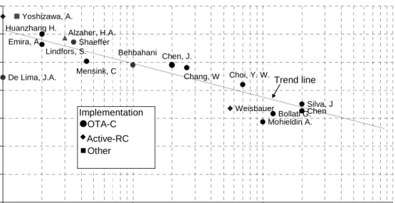
The FoM does not consider other parameters such as the quality factors (Q) or other additional features that a reported filter may have, but it gives an indication of the trend of this technology. Figure 1.6 shows FoM vs. frequency of operation for the most recent journal filter publications [10]-[24]. There is a decaying trend line as frequency increases because there is more integrated thermal noise and many linearity techniques cannot be applied for higher frequencies efficiently. The dynamic range depends on the frequency of operation; also reported linearization techniques are not very effective at higher frequencies.
It is interesting to see that most of the reported high frequency techniques use OTAs. This is due to the fact that OTA-C implementations are simpler for frequencies of tenths of MHz and more reliable in terms of stability if compared to Active-RC.
Arising technologies require higher circuit performances and this is the case for analog interfaces requiring continuous time filters. For instance, in ADSL (Asymmetrical Digital Subscriber Lines) cable modem applications, the linearity has to be better than 60dB [25]-[26] and video applications require at least 60 dB of linearity
at 5 MHz [27]. Future trends pushing towards higher data transfers will require higher frequency ranges with equal or better linearity.
Mohieldin A. Silva, J Chen Yoshizawa, A. Weisbauer Bollati G. Shaeffer De Lima, J.A. Alzaher, H.A. Huanzhang H. Behbahani Emira, A. Choi, Y. W. Lindfors, S. Mensink, C Chang, W Chen, J. 0 10 20 30 40 50 60 70 1 10 100 1000 Frequency (Mhz) Fo M Implementation zOTA-C Active-RC Other Trend line
Fig. 1.6 Figure of merit of recent publications about filters.
1.4 Contributions
In this dissertation, three techniques for the design of high dynamic range OTA-C filters are proposed. These techniques are based in the linearization of the most important contributor to the distortion in the OTA: The differential pair.
First, the double differential pair is introduced where the distortion due to one differential pair is cancelled by the auxiliary circuit. If properly dimensioned and biased, the double differential pair offers an advantage of more than 10dB of linearity for the same power consumption and transconductance compared to the typical differential pair
with a very small noise 1-2dB increase. An OTA based on the double differential is presented featuring 25% continuous transconductance tuning with minimal linearity degradation. The OTA is tested in a 20-MHz second order low-pass ladder filter prototype. With a 10.5mW of power per OTA, the filter achieves -65dB IM3 for 1.3Vpp.
The second proposed technique is a triple differential pair architecture. it offers a more robust linearity cancellation with the drawback of reduced transconductance per power. Experimental results for an OTA fabricated in the TSMC 0.35µm CMOS process are presented and compared with recently reported topologies. Draining 2.8mA from a single supply voltage of 3.3V, the transconductor achieves IM3<-70dB for a two-tone input signal of 1.3Vpp measured at 70 MHz. The input referred noise density is only 7nV/√Hz, leading to a SNR of 75dB.
Finally, the non-linear source degeneration differential pair is presented. The linearity of a typical source degenerated structure is improved by more than 10 dB while the overall small signal transconductance is reduced by less than 10%; the additional power needed by the auxiliary circuitry is less than 10 % of the OTA’s power, and the noise level increases by no more than 1 dB. A self-bias circuit is used to match the transconductance to polysilicon resistor values serving two purposes: i) ensuring the linearity of the OTA against process parameter variations and ii) allowing the use of polysilicon resistors for filter’s terminations. The technique is tested in a 30MHz 5th order elliptic filter consuming 85mW of static power and achieving a spurious free dynamic range (SFDR) of 65dB. With these results, this filter is 6dB above the trend
line shown in figure 1.6. An automatic frequency tuning circuit to is included to reduce the low-pass frequency cut-off with process parameter variations.
1.5 Organization
Section 2 starts by describing the main noise and linearity issues of a simple differential pair. Then, the double differential pair is introduced and studied. A full OTA design using the double differential is described and incorporated in a second order 20-MHz low-pass filter. Simulated and experimental results are included. Finally, the triple differential pair is analyzed. Simulation and experimental results are shown and are compared with previously reported topologies.
Section 3 discusses the non-linear source degeneration technique. A 30-MHz elliptic low-pass filter design is presented suitable for next generation Power Line Communication Systems. Details of the OTA, filter tuning, automatic bias and other issues are addressed. The design of an automatic tuning circuit is explained. Experimental results are shown and compared with previous publications. Finally, section 4 presents the conclusions and summarizes the contributions of this work.
2. LINEARITY ENHANCEMENT TECHNIQUES BASED ON NON-LINEARITY CANCELLATION
Distortion occurs in the voltage to current conversion due to the non-linear behavior of transistors in the differential pair. The first part of this section addresses the linearity and noise issues of the differential pair. Then, the techniques based on non-linearity cancellation are presented: The double differential pair and the triple differential pair. The double differential pair is discussed and an OTA and filter implementation is presented. The last part of the section discusses the triple differential pair and describes simulation and experimental results.
2.1 The differential pair
The differential pair is the most popular structure used in the implementation of differential OTAs (Figure 2.1). One of the more important properties of the differential pair is that it has a very good rejection to common mode signals; however the linearity is limited due to the tail current transistor. In this subsection the analysis of distortion and noise of the differential pair is presented. The outcomes are used as the basis for the evaluation of the proposed techniques.
v
g1v
g2
i
d1i
d2I
TFig. 2.1. The differential pair.
2.1.1 Distortion
For a MOS transistor working in saturation, the drain current is given by:
2
)
( g s T
d K v v V
i = − − (2.1)
where VT is the threshold voltage and K is a physical constant given by:
= L W C K µ ox 2 1 (2.2)
W and L are the width and length of the transistor respectively; µ is the mobility of carriers (electrons for N-type transistors and holes for P-type transistors) and Cox is
the oxide capacitance per unit area.
For the differential pair shown in fig. 2.1, the input voltage of each transistor is:
2 2 2 1 in cm g in cm g v v v v v v − = + = (2.3)
where vcm is the common mode voltage and vin the differential input voltage. Defining
vc=vcm-vs-VT and using (2.2), id1-id2 is given by:
c in d
d i Kv v
i 1− 2 =−2 (2.4)
Due to the current source, the sum of id1 and id2 must be equal to IT, then:
+ = = + 2 2 2 1 4 2 in c T d d v v K I i i (2.5)
Solving for vc in (2.5) and using the outcome in (2.4) yields:
4 2 2 2 2 1 in T in d d v K I Kv i i − = − (2.6)
Defining differential current as io=(id1-id2)/2, (2.6) can be expressed as:
2 2 4 1 2 dssat in in m o V v v g i = − (2.7)
where gm is the transconductance of the transistor given by:
dssat
m KV
g =2 (2.8)
and Vdssat is the DC saturation voltage given by:
K I V V V V T T S G dssat = − − = (2.9)
For a simplified distortion analysis, the above expression can be expanded in taylor series around vin=0, such that:
∑
= + + ⋅ = 0 1 2 ) 1 2 ( n n in n M o G v i (2.10) where,1 ) 1 ( 2 2 − − = j dssat j m Mj V g G (2.11)
GM1 is the linear coefficient and GM3,GM5,… are undesired non-linear terms.. For
weak signals, the distortion is mainly produced by the third order term; therefore higher terms can be ignored leading to:
3 3 1 in m in m o G v G v i ≈ + (2.12)
The linearity can be measured in terms of intermodulation distortion. Two sinusoidal tones are used for the input such that:
( )
t A( )
t A vin 1 cos 2 2 cos 2 ω + ω = (2.13)where A is maximum amplitude and ω1 and ω2 are the angular frequencies of
each tone. Using (2.13) in (2.12) and trigonometric identities, one arrives at:
( )
( )
(
)
(
)
(
)
(
)
(
)
(
)
(
)
(
t t)
A G t t t t A G t t A G A G i M M M m o 2 1 3 3 1 2 2 1 1 2 2 1 3 3 2 1 3 3 1 3 cos 3 cos 32 ) 2 ( cos ) 2 ( cos ) 2 ( cos ) 2 ( cos 32 3 cos cos 32 9 2 ω ω ω ω ω ω ω ω ω ω ω ω + + + + + + − + − + + + = (2.14)The second term contains the intermodulation products. Since these components are caused by the third order term in (2.12) it is referred as the third order
intermodulation distortion symbolized IM3 and it is measured as the power ratio of one of the intermodulation products to one fundamental tone. Therefore:
32 9 2 32 3 3 3 3 1 3 3 A G A G A G IM M m M + = (2.15)
Since GM3 is usually very small compared to GM1, then:
1 2 3 16 3 3 m M G A G IM = (2.16)
Applying (2.11) in (2.16) results in:
2 2 128 3 3 dssat V A IM = (2.17)
According to (2.17), using larger Vdssat yields a better linearity. However, in
order to keep all the transistors working in saturation, Vdssat has to be limited as shown in
fig. 2.2 to: ) ( ) ( 2 1 cm ss dsat T dssat V V V V V < − − + (2.18) B V
V
cmV
cmV
CV
C>V
dssat2V
SSM1
M1
M2
To further reduce the distortion, a resistor connected between the sources of transistors M1 and M2 can be used as shown in fig. 2.3. To simplify the analysis, the middle node of the resistor is referred as vr, then the voltage at the sources of M1 and
M2 is. 2 1 res r s v v v = + (2.19) 2 2 res r s v v v = − (2.20)
where vres is the voltage drop across the resistor. Using (2.1), (2.19) and (2.20) the drain
currents are: 2 1 ) 2 2 ( res T r in cm d V v v v V K i = + − − − (2.21) 2 2 ) 2 2 ( res T r in cm d V v v v V K i = − − + − (2.22)
v
g1v
g2i
d1i
d2v
rV
BV
BI
T/2
I
T/2
R/2
R/2
Defining vc=Vcm-vr-VT, and following the same procedure as (2.4) to (2.7), one arrives at: 2 2 4 ) ( 1 2 ) ( dssat res in res in m o V v v v v g i = − − − (2.23)
where the taylor expansion is given by:
∑
∞ = + + ⋅ − = 0 1 2 ) 1 2 ( ( ) n n res in n M o G v v i (2.24)Notice that the only difference between (2.24) and (2.10) is that vres is subtracted
to vin. The current passing through the resistance is ires= id1-IT /2 = -(id2-IT/2); Clearing IT
yields, o d d res i i i i = − = 2 2 1 (2.25) Then the voltage across the resistance is:
R i
vres = o (2.26)
If (2.26) is used in (2.23), a fourth order equation would result that can be very complex and tedious to solve io in terms of vin. An alternative is to obtain the solution
directly in a series expansion which for the purpose of studying the linearity is more useful. The solution in a series expansion can be expressed as:
∑
∞ = + + = 0 1 2 1 2 k k in k o C v i (2.27)where Ck are unknown coefficients. To find these, (2.27) can be plugged in (2.24)
∑
∑
∑
∞ = + ∞ = + + + ∞ = + + = ⋅ − 0 1 2 0 1 2 1 2 ) 1 2 ( 0 1 2 1 2 ( ) n n k k in k in n M k k in k v G v R C v C (2.28)Notice in the right hand expression that terms in the summatory with vin will only
be produced when n=0, terms with vin3 when n=0 and n=1, terms with vin5 with n=0, n=1 and n=2. Therefore, if we are only interested to solve C1,C3 and C5 we can perform
the summatory up to n=2 and k=2 and ignore terms elevated to a power higher than five. Then, (2.28) becomes: 5 5 5 3 3 1 5 3 5 5 3 3 1 3 5 5 3 3 1 1 5 5 3 3 1 ) ) 1 (( ) ) 1 (( ) ) 1 (( in in in M in in in M in in in M in in in v RC v RC v RC G v RC v RC v RC G v RC v RC v RC G v C v C v C − − − + − − − + − − − = + + (2.29)
Expanding and ignoring terms vin with order higher than five yields,
(
)
(
)
(
(
)
)
(
(1 ) 3 (1 ) (1 ))
0 1 1 5 1 5 3 2 1 3 5 1 3 3 1 3 1 3 1 1 1 = − + − + + + − + + − + in M M M in M m in M M v RC G RC RC G C R G v R C G R G C v G C R G (2.30)For this equation to hold, each of the coefficient has to be zero, then it is straightforward to solve C1, the C3 and finally C5, thus:
) 1 ( 1 1 1 M M RG G C + = (2.31) 4 1 3 3 ) 1 ( M M RG G C + = (2.32) 7 1 2 3 5 1 5 5 ) 1 ( ) 3 ( M M M M M RG G G G R G C + − + = (2.33)
5 7 1 2 3 5 1 5 3 4 1 3 1 1 ) 1 ( ) 3 ( ) 1 ( ) 1 ( M in M M M M in M M in M M o v RG G G G R G v RG G v RG G i + − + + + + + = (2.34)
For weak non-linearities, the third term is higher than the fifth order term being the larger contributor to distortion, then using (2.13) in (2.34) results in:
3 2 2 ) 1 ( 128 3 3 r dssat N V A IM + = (2.35)
where Nr is the degeneration factor given by Nr=GM1R. Higher degeneration factors
improve the linearity at the cost of reduced linear transconductance given by:
) 1 ( 1 r M M N G G + = (2.36) 2.1.2 Noise
Figure 2.4 presents the degenerated differential pair with all the equivalent noise sources. B V VB
v
g1v
g2M2
M2
M1
M1
i
n12i
n22i
r2Each noise source is given by: 1 2 1 4 m n g kT Hz i = γ (2.37) 2 2 2 4 m n g kT Hz i γ = (2.38) R kT Hz ir2 4 = (2.39)
where k is the Boltzman constant, T the temperature, γ is typically in the range of 0.7 to 2, gm1 and gm2 the transconductance of M1 and M2 respectively. The total output noise
current can be found as:
+ + + + + = 2 2 1 2 1 2 1 2 1 1 2 1 2 ) 2 ( ) ( 2 ) 2 ( ) 2 ( 2 4 m m m m m m m no g R g R g R g R g g R g kT Hz i γ γ (2.40)
Using the definition in (2.11) where GM1=gm1/2, yields:
+ + + + + = 2 2 1 2 1 2 1 2 1 1 2 1 2 ) 1 ( ) ( 2 ) 1 ( ) 1 ( 1 4 m M M M m M M no g R G R G R G R G G R G kT Hz i γ γ (2.41)
Since Nr=GM1R, the input referred noise is:
+ + = + = 1 2 2 1 2 2 1 2 2 2 4 ) 1 ( m m r r m r m no no G g N N G kT N G Hz i Hz v γ γ (2.42)
The third term inside the parenthesis is due to the noise of the tail current sources. This term can be minimized by reducing gm2 with respect to Gm1. However, this
the noise due to the tail current is equally injected to both branches appearing as common-mode rather than differential.
I
Tv
g1v
g2
I
T/2+i
oI
T/2-i
o+ V
r-
- V
r+
Fig. 2.5. Pseudo-differential pair with the tail current in the middle.
The input referred noise density of the DP of fig. 2.5 is then given by:
(
r)
m in N G kT v = γ + 1 2 4 (2.43)The disadvantage of this topology is that there is a DC voltage drop due to the current IT passing through the resistors given by:
4
R I
V T
r = (2.44)
This voltage drop limits the voltage headroom for Vdsaat1 and Vdssat2 and therefore Nr must be limited.
From the analysis shown here, it can be seen that the distortion can be improved by using larger Vdssat1 but the supply voltage limits this value. The increase of the
degeneration factor (Nr) is then a good alternative for improved linearity but the drawback is that excessive degeneration factors reduce the total transconductance (for the same amount of power) and increase the noise.
2.2 The double differential pair
The double differential pair consists of two differential pairs with cross-coupled outputs such that the third order distortion components are cancelled. The following sub-sections present the analysis and performance comparison with the conventional simple differential pair.
2.2.1 Analysis
Figure 2.6 shows the double differential pair where the total output is given by,
2 1 o o
oT i i
B V VB M1 M1 M3 M3 VB VB M2 M2 M4 M4
R
1R
2 VSS VSS IT1/2 IT1/2 IT2/2 IT2/2 (IT1+IT2)/2+ioT (IT1+IT2)/2-ioTv
in+v
in-IT1/2-io1 IT1/2+io1 IT2/2+io2 IT2/2-io2
Fig. 2.6. The double differential pair.
Based on (2.34), io is then given by (the fifth order component is neglected for
simplicity): 3 4 2 2 , 3 4 1 1 , 3 2 2 , 1 1 1 , 1 ) ) 1 ( ) 1 ( ( ) ) 1 ( ) 1 ( ( in r M r M in r M r M oT v N G N G v N G N G i + − + + + − + = (2.46)
For cancellation of the third order component, which is the main contribution to distortion component, the following condition has to be met,
4 2 2 , 3 4 1 1 , 3 ) 1 ( ) 1 ( + = r + M r M N G N G (2.47) Using (2.8) and (2.2), the above expression can be presented as:
3 2 1 8 2 2 2 2 1 1 1 1 2 1 ) / ( ) / ( ) ( 2 ) ( 2 = + + + + L W L W R R K I R R K I I I T T T T θ θ (2.48)
Equation (2.48) also includes an additional resistance Rθ in series with the degeneration resistance to consider the mobility degradation effect. This effect has an important contribution in the linearity, especially for small channel lengths. The equivalent resistance due to mobility degradations [28] is:
ox oC L W R µ θ θ = (2.49)
where µ0 is the low-field mobility and θ the mobility constant given by:
T c E L θ θ + ⋅ = 1 (2.50)
The first term of (2.50) represents the mobility degradation due to the lateral electric field where Ec is the lateral critical electric field. θT is a fitting parameter to also
consider the mobility due to the transversal electric field. Typical values of θ are in the order of 0.3 V-1 to 2 V-1 for sub-micron technologies.
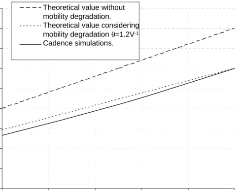
To corroborate (2.48), the circuit of fig. 2.6 was simulated using Cadence with the following values: (W/L)1=20µm/1µm, (W/L)1=40µm/1µm, µCox=120µA/V, R1=2kΩ
and R2=500Ω. Figure 2.7 shows the IM3 vs. IT2 for an input voltage of 200mVpp around
20MHz for three different IT1. A fourth curve depicted with a wide line shows the IM3
of the larger differential pair for reference. Notice that for the three values of IT1 there is
a IT2 at which IM3 is improved by almost 20dB. To verify that (2.48) agrees with
linearity is achieved. Notice that if mobility degradation is not considered (eg Rθ1=Rθ2=0), (2.48) significantly deviates from simulated results. This is due to the fact
that the term in the parenthesis of the left-hand side of (2.48) is elevated to the power of eight and any small variations, such as the mobility degradation resistance, produce a significant deviation. However, if mobility degradation is considered (θ=1.2V-1), then (2.48) is close to the simulation result.
-90 -85 -80 -75 -70 -65 -60 -55 -50
0.00E+00 5.00E-04 1.00E-03 1.50E-03 2.00E-03
It1=100uA It1=150uA It1=200uA It1=0 IM3 IT2(mA)
0 200 400 600 800 1000 1200 1400 1600 1800 100 120 140 160 180 200 IT1 IT 2
Theoretical without mobility degradation Theoretical considering mobility degradation Cadence simulations
I
T1(
µ
A)
I
T2(
µ
A)
Theoretical value without mobility degradation.
Theoretical value considering mobility degradation θ=1.2V-1
Cadence simulations.
Fig. 2.8. Relation between IT1 and IT2 for optimal linearity.
As shown in the above analysis, to effectively suppress the third order component, one must consider θ. Similar reported structures that do not consider the mobility degradation effect are subject to large errors and the linearity improvement may not be optimal. Even if considered, the mobility degradation factor θ is a process dependent parameter and cannot be accurately predicted nor controlled.
2.2.2 Improvement comparison
Since the outputs of the differential pairs are subtracted, the effective transonductance GmT of the DDP is reduced by:
) 1 ( ) 1 ( 2 2 , 1 1 1 , 1 + − + = r M r M MT N G N G G (2.51)
In addition, the noise increases due to the contribution of both differential pairs and additional current sources. Adding all noise components it can be shown that the input referred noise of the DDP is:
2 1 2 2 2 2 2 1 2 4 2 2 2 2 2 1 1 3 2 1 1 2 2 1 2 ) 1 ( ) 1 ( 2 ) 1 ( 2 ) 1 ( 4 r M r M m m r r r M m m r r r M no N G N G G g N N N G G g N N N G kT Hz v + − + + + + + + + + = γ γ γ γ (2.52)
Although the DDP presents reduced harmonic distortion, the transconductance is decreased and noise increases. Then, it is not clear if there is a real improvement in the overall signal to noise ratio compared to the conventional simple differential pair (SDP). To this end, a simulation was performed to give to compare the DDP and the SDP for the same power consumption and the same transconductance (Fig. 2.9). The SDP is designed to use the same Vdsat as the transistors in the DDP but it uses a larger degeneration factor in order to present equal transconductance.
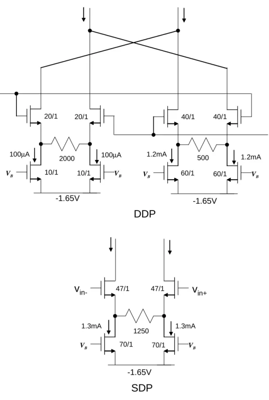
B V VB VB VB 2000 500 -1.65V
v
in+v
in-B V VB 47/1 47/1 1250v
in-v
in+ -1.65V -1.65V 20/1 20/1 40/1 40/1 10/1 10/1 70/1 70/1 60/1 60/1DDP
SDP
100µA 100µA 1.2mA 1.2mA 1.3mA 1.3mAFig. 2.9. SDP and DDP designs for comparison with same transconductance, Vdsat and power consumption.
Table 2.1 presents the main design parameters for both circuits. The degeneration factor for the SDP is higher by 2.5 times in order to achieve the same transconductance as the SDP. This larger Nr improves the distortion of the SDP but also increases the input referred noise due to the tail current transistors resulting in just a slightly smaller input referred noise density compared to the DDP. The transconductance for both structures is 500µA/V.
Table 2.1. Results for the comparison between SDP and DDP.
Parameter SDP DDP
Degeneration factor 1.75 0.75
Vdsat 350mV 350mV
Input referred noise density 6.8nV/Hz 7.8nV/Hz
Current consumption 1.4mA 1.4mA
Transconductance 500µA/V 500µA/V
Both structures in fig. 2.9 were simulated for different input amplitudes and the IM3 was measured. Fig 2.10 shows a plot of the linearity improvement of the DDP over the SDP (IM3SDP-IM3DDP) for the same SNR. The SNR was calculated for a bandwidth
of 10MHz. Up to 60dB of SNR, the DDP achieves more than 10dB of linearity improvement over the SDP. However as the input signal is larger (In this example SNR>60dB), the linearity improvement worsens due to the fifth order non-linearities caused by the smaller Vdsat differential pair used in the DDP.
SNR
IM3
SD P-IM3
DD P -10 -5 0 5 10 15 20 40 60 80 100Fig. 2.10. Improvement in IM3 of the DDP over the SDP.
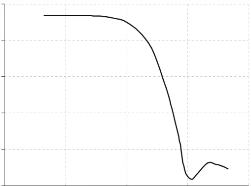
The frequency limits to achieve high linearity are mainly dictated by the decay of degeneration resistance due to effective parasitic capacitances at the source of transistors M1. If Cs is the parasitic capacitance at the source of transistors M1, the frequency limit to hold the linearity is approximately wl=2/(RCs) where R is the degeneration resistor. Figrure 2.11 shows the IM3 plot vs. frequency for the circuit in figure 2.9.
-90 -80 -70 -60 -50
1.E+06 1.E+07 1.E+08 1.E+09
Frequency (Hz)
IM
3
Fig. 2.11 IM3 plot vs. frequency.
2.3 A 20 MHz second order low-pass filter
The double differential technique is used in an OTA-C low-pass filter ladder prototype to verify its application. The following subsections describe the OTA and filter design. At the end of this subsection, experimental results are presented.
2.3.1 OTA design
Figure 2.12 shows the overall OTA design. For the input stage, the double differential pair is used in order to achieve the non-linearity cancellation as described in
the previous section. Transistors M1 and M2 use a Vdsat a 280mV and 330mV,
respectively, and the degeneration factors are Nr=1.
cmb cmb vn vn IT1 R1 R2 IT2 vp Vgm -Vgm+ io -io+ vi+ vi -vo- vo -1 L W 2 L W rm1 rm2 rm2 Vb1 Vb2 Vb3 Vb3 VDD VSS
Fig. 2.12 OTA design.
A transconductance control is incorporated in order to provide frequency tuning for the filter. For that matter, the variation of IT1 and IT2 is not a good option because it
modifies Vdsat1 and Vdsat2 changing the linearity properties and also it affects the optimal
linearity cancellation point. To provide independent transconductance control while maintaining a constant linearity, a current division approach is used as described in [26],[29]. Tail currents IT1 and IT2 are fixed and optimized for best linearity, and the
transconductance is varied with the aid of triode operating transistors M3 and M4. The output current of the DDP is attenuated by a factor α which is given by:
4 3 3 2 m m m r r r + = α (2.53)
where rm3 and rm4 are the resistance values of the triode region operating transistors M3
and M4, respectively. These resistances are given by:
(
)
1 3 3 3 2 ( ) − − = m gs T m K V V r (2.54)(
)
1 4 4 4 2 ( ) − − = m gs T m K V V r (2.55)Since the gate voltages of M3 and M4 are controlled by Vgm+ and Vgm-, α is a
function of Vgm+ - Vgm-. Equation (2.53) holds provided that the voltage at the source of
M6 remains almost constant for any current changes thus it is desired to have a large gm6. To accomplish this an inverter formed with transistors M9 and M10 provide a
negative voltage gain from the source to the gate of M6 boosting its transconductance to A*gm6; A is the gain of the inverter composed by transistors M9 and M10 which in this case is around 30dB. Transistors M5-M8 form a regulated cascode output stage to enhance the output resistance.
The dimensions of the transistors were chosen using the following considerations: M1 and M2 were dimensioned to achieve 280mV and 330mV with bias currents of 250µA and 330µA which results in the optimal linearity condition. Transistors M3 and M4 are designed using (2.54) and (2.55) to obtain resistances in the order of 500 ohms for optimal noise performance. The current through the transistors cascode transistors M6,M7 and M8 uses the same bias current as It1 and It2 for minimum power consumption yet enough to supply current at maximum output swings. M11 supply 1mA of current and are designed to keep a Vdsat of less than 500mV to
allow the swing at nodes x and y. Table 2.2 shows the final transistor dimensions of the OTA.
Table 2.2. Transistor sizes for the OTA. Length for all transistors is 1µm.
Transistor Width (µm) Id (µA) M1 20 250 M2 40 330 M3 20 0 M4 40 0 M5 80 230 M6 160 455 M7, M8 40 450 M9 60 200 M10 80 200 M11 80 1000
The noise at the output of the OTA is a combination of the noise of the OTA core (transistors M1 and M2), the resistor divider (M3 and M4) and the cascode transistors. The approximate output thermal noise density of the OTA is given by:
+ + + + + + + + ⋅ + + + + + = 2 2 2 2 2 2 2 2 1 1 2 1 1 1 2 2 10 10 9 2 11 5 8 2 ) 1 ( ) 1 ) 2 /( ( ) 1 ( ) 1 ) 2 /( ( 2 ) ( 4 8 r mT r m r r mT r m r a a m m m m m m o N g N g N N g N g N r r g g g g g g kT Hz I γ γ α γ α γ (2.56)
where rα=rm3+2rm4. There are several observations in this expressions: the larger rα the
lower the noise but a large increase in these resistances brings the parasitic pole wp=1/(αrm4Cp) to lower frequencies limiting OTA’s frequency response; Cp is the overall
parasitic capacitance at the nodes x and y. The noise of transistors M9 and M10 is attenuated by the gain A=gm10ra which is around 30, therefore its noise contribution is
not important.
2.3.2 Filter design
Wire line applications, such as VDSL, contemplate next generation bandwidths up to 20MHz. To test the double differential pair concept, a 20MHz second order low-pass filter is designed. The filter is based on a ladder prototype presented in fig. 2.13.
R
2C
1V
1L
1R
1V
oV
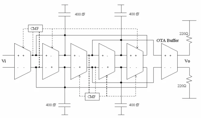
iThe filter is simulated using five identical OTAs as shown in Figure 2.14. The OTA transconductance can be adjusted between 70 to 160µA/V; The capacitor values are 400 fF each. An output buffer based on the same OTA is used to measure the output voltage. Due of the differential nature of the OTAs, common mode feedback (CMF) blocks are used to keep the output stages balanced around the reference voltage.
Fig. 2.14. Low-pass OTA implementation of the ladder filter.
The relation between (R1+Rθ1) and (R2+Rθ2) in (3.32) can varies from die to die
(process variations) because of tolerances in both sheet resistance (used to implement the polysilicon resistance) and mobility degradation factor. An extra test OTA (TOTA) is used to provide information about the linearity as illustrated in fig. 2.15. Based on this, a
fine bias external adjustment is possible; since all OTA's used in the filter are the same, the adjustment of the bias condition for maximum linearity in the TOTA optimizes the linearity of the overall filter as well. For testing purposes, the linearity observation of the TOTA is done by applying two tones at the input and measure the IM3 using a spectrum analyzer at the output. For future versions, on-chip precision circuits (such as switched capacitor) are contemplated to implement the linearity adjustment in automatically.
Fig. 2.15. Linearity adjustment using a test OTA (TOTA).
2.3.3 Experimental results
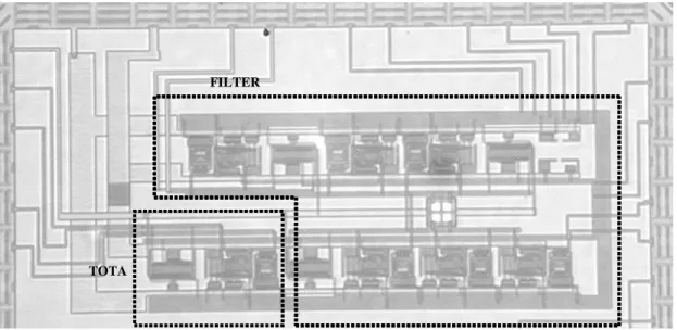
Figure 2.16 shows the micrograph of the chip where the active area is 0.45mm2. The chip was fabricated in a standard CMOS 0.35µm process through the MOSIS educational service. In the test set-up, waveform generators are used to provide the input
signals and a balun is used to convert them from single-ended to differential. At the output, 50 ohm resistances are used as load for the OTA buffer and another balun is used to convert the differential output signal into single-ended; the signal is then analyzed using a spectrum analyzer.
TOTA
FILTER
Fig. 2.16. Micrograph of the chip.
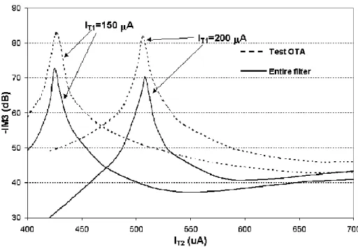
Two sinusoidal tones separated by 100kHz around 20MHz with a total amplitude of 1.3 Vpp were used to test the circuits. Figure 2.17 shows the IM3 of the TOTA and the entire filter as function of the current IT2; IT1 has been fixed at 150 µA and 200 µA,
respectively. The tail current at which optimal IM3 is achieved for the TOTA optimizes the linearity of the entire filter as well.
Fig. 2.17. IM3 of the filter and TOTA for several currents IT1 and IT2.
The IM3 measurement of the TOTA is below -70dB for the whole range of frequencies up to 50 MHz. Figure 2.18 shows the effect of the transconductance control on IM3. The transconductance can be controlled from 70 µA/V to 160 µA/V and IM3 is better than -70 dB. This corroborates that the transconductance control is indeed almost independent of linearity.
Figure 2.19 shows the IM3 measurement at 20MHz for the filter at 1.3Vpp input. Here, IM3 remains below -65dB over the entire filter’s pass-band. The transconductance control allows to change the cut-off frequency from 12 to 24 MHz as shown in figure 2.20. The noise floor that can be appreciated at high frequencies is caused by parasitic capacitances present in the circuit board. Table 2.3 summarizes experimental results of the TOTA and the filter.
40 50 60 70 80 90 -0.4 -0.2 0 0.2 0.4 0.6 0.8 1 Control voltage (V) -I M3 ( d B ) 6.0E-05 8.0E-05 1.0E-04 1.2E-04 1.4E-04 1.6E-04 Tr a n s c ondu c ta n c e ( A /V )
Fig. 2.18. Effect of the transconductance control over the IM3.
-30 -20 -10 0 10 1 10 100 Frequency (Mhz) Ma g n itu de (d B )
Fig. 2.20. Programmable frequency responses of the filter.
Table 2.3. Summary of experimental results of the filter.
Technology. CMOS 0.35 µm
Supply voltage. 3.3 V
OTA
Power consumption per OTA. 10.5 mW Transconductance range. 70 – 160 µA/V OTA IM3
up to 50MHz @1.3Vpp input. <-70dB Input referred noise 75 nV/√Hz
SNR @ 20 MHz 62 dB
Filter
Filter’s IM3 at 20MHz
PSRR+, PSRR- >50 dB
Input referred noise 6 µV/√Hz SNR of the filter. (20 Mhz bandwidth) 55 dB
For the purpose of comparing the filter performance with reported schemes, the same figure of merit as defined in (1.2) will be used. Figure 2.21 shows where the described filter stands in reference to others. The proposed scheme, however, has several features that other filters do not:
• Due to the transconductance control incorporated with transistors M3 and M4, there is a nominal loss of half the transconductance because part of the output differential current flows intro transistor M3 rather. However, this feature allows a large continuous tuning range of about ±30% with minimal linearity degradation.
• Thanks to the regulated cascode output stage, the output resistance is considerably large; therefore this OTA can be used for high-Q applications. The drawback, is that the regulated cascode stage consumes 6mW which is 60% of the overall OTA power. Without the regulated cascode stage, the filter would consume half the power at the expense of lower output impedance.
Although the OTA require power consumption and has increased noise to incorporate the above mentioned features, it is still on the trend line in filters thanks to the proposed linearity techniques using the DDP.
Mohieldin A. Silva, J Chen Yoshizawa, A. Weisbauer Bollati G. Shaeffer De Lima, J.A. Alzaher, H.A. Huanzhang H. Behbahani Emira, A. Choi, Y. W. Lindfors, S. Mensink, C Chang, W Chen, J. Proposed filter 0 10 20 30 40 50 60 70 1 10 100 1000 Frequency (Mhz) Fo M Implementation zOTA-C Active-RC Other Trend line
Fig. 2.21. Figure of merit of the filter in comparison with the state of the art in filters.
2.4 The triple differential pair 2.4.1 Analysis
It has been shown that the double differential can be used to reduce OTA non-linearities but the optimal cancellation is very sensitive to process variations and requires external adjustment. This is due to the fact that the cancellation relies on matching physical parameters such as Vdsat, Rθ and Gm that cannot be accurately controlled or
predicted.
The alternative is to use equal DPs with same linear properties but different input voltages. This can be done exploiting the differential nature of the DPs; if one of the inputs of the DP is grounded, the output will be the function of half of the input voltage.
Figure 2.22 shows the block diagram of one degenerated differential pair split in three. The three DPs use the same saturation voltage and equal degeneration factors but different transistor aspect ratios. Two of the DP’s (most left and most right) have one of the input terminals connected to ground and, due to the differential nature of DPs, their output current is a function of both differential and common-mode input signal. The overall circuit, however, behaves as a true differential circuit because any common mode input produces differential output current in the DPs with one terminal grounded, but due to the cross-coupled connection they cancel each other. The third DP located at the middle, is connected to both inputs as a conventional DP with tail current and uses the full input signal.
+
_
+
_
+
+
_
_
+
+
_
_
v
in-
v
in+
4/9
1/9
4/9
i
oi
oFig. 2.22. The triple differential pair block diagram.
For the analysis of the topology, it is considered that the input signals are composed by differential and common-mode signal components such as vin+= vin/2 + vcm