Wireless Integrated Network Sensors: Low Power Systems on a Chip
G. Asada, M. Dong, T. S. Lin, F. Newberg, G. Pottie, W. J. Kaiser,
University of California, Los Angeles, Los Angeles, California
kaiser@ee.ucla.edu
and
H. O. Marcy
Rockwell Science Center, Thousand Oaks, California
Abstract
Wireless Integrated Network Sensors (WINS) now provide a new monitoring and control capability for transportation, manufacturing, health care, environmental monitoring, and safety and security. WINS combine sensing, signal processing, decision capability, and wireless networking capability in a compact, low power system. WINS systems combine microsensor technology with low power sensor interface, signal processing, and RF communication circuits. The need for low cost presents engineering challenges for implementation of these systems in conventional digital CMOS technology. This paper describes micropower data converter, digital signal processing systems, and weak inversion CMOS RF circuits. The digital signal processing system relies on a continuously operating spectrum analyzer. Finally, the weak inversion CMOS RF systems are designed to exploit the properties of high-Q inductors to enable low power operation. This paper reviews system architecture and low power circuits for WINS.
1.
Introduction
Wireless integrated network sensors (WINS) combine sensing, signal processing, decision capability, and wireless networking capability in a compact, low power system. Compact geometry and low cost allows WINS to be embedded and distributed at a small fraction of the cost of conventional wireline sensor and actuator systems. For example, on a global scale, WINS will permit monitoring of land, water, and air resources for environmental monitoring. On a national scale, transportation systems, and borders will be monitored for efficiency, safety, and security. On a local, wide-area scale, battlefield situational awareness will provide personnel health monitoring and enhance security and efficiency. Also, on a metropolitan scale, new traffic, security, emergency, and disaster recovery services will be enabled by WINS. On a local, enterprise scale, WINS will create a manufacturing information service for cost and quality control. WINS for biomedicine will connect patients in the clinic, ambulatory outpatient services, and medical professionals to sensing, monitoring, and control. On a local machine scale, WINS condition based maintenance devices will equip powerplants,
appliances, vehicles, and energy systems for enhancements in reliability, reductions in energy usage, and improvements in quality of service.
The opportunities for WINS depend on the development of a scalable, low cost, sensor network architecture. This requires that sensor information be conveyed to the user at low bit rate with low power transceivers. Continuous sensor signal processing must be provided to enable constant monitoring of events in an environment. Thus, for all of these applications, local processing of distributed measurement data is required for a low cost, scalable technology. Distributed signal processing and decision making enable events to be identified at the remote sensor. Thus, information in the form of decisions is conveyed in short message packets. Future applications of distributed embedded processors and sensors will require massive numbers of devices. Conventional methods for sensor networking would present impractical demands on cable installation and network bandwidth. By eliminating the requirements for transmission of all measured data, the burden on communication system components, networks, and human resources are drastically reduced.
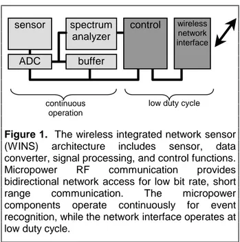
Figure 1. The wireless integrated network sensor (WINS) architecture includes sensor, data converter, signal processing, and control functions. Micropower RF communication provides bidirectional network access for low bit rate, short range communication. The micropower components operate continuously for event recognition, while the network interface operates at low duty cycle.
sensor ADC spectrum analyzer buffer control wireless network interface continuous operation
2.
Wireless Integrated Network Sensor
(WINS) System Architecture
The primary limitation on WINS node cost and volume arises from power requirements and the need for battery energy sources. As will be described, low power sensor interface and signal processing architecture and circuits enable continuous low power monitoring. However, wireless communication energy requirements present additional severe demands. Conventional wireless networks are supported by complex protocols that are developed for voice and data transmission for handhelds and mobile terminals. These networks are also developed to support communication over long range (up to 1km or more) with link bit rate over 100kbps.
In contrast to conventional wireless networks, the WINS network must support large numbers of sensors in a local area with short range and low average bit rate communication (less than 1kbps). The network design must consider the requirement to service dense sensor distributions with an emphasis on recovering environment information. The WINS architecture, therefore, exploits the small separation between WINS nodes to provide multihop communication.
Multihop communication (see Figure 2) yields large power and scalability advantages for WINS networks. First, RF communication path loss has been a primary limitation for wireless networking, with received power, PREC, decaying as transmission range, R, as PREC∝ R
-α (where α varies from 3 – 5 in typical indoor and outdoor environments). However, in a dense WINS network, multihop architectures may permit N communication link hops between N+1 nodes. In the limit where communication system power dissipation (receiver and transceiver power) exceeds that of other systems within the WINS node, the introduction of N co-linear equal range hops between any node pair reduces power by a factor of Nα-1 in comparison to a single hop system. Multihop communication, therefore, provides an immediate advance in capability for the WINS narrow bandwidth devices. Clearly, multihop communication raises system complexity. However, WINS multihop communication networks permit large power reduction and the implementation of dense node distribution.
3.
WINS Node Architecture
The WINS node architecture (see Figure 1) is developed to enable continuous sensing, event detection, and event identification at low power. Since the event detection process must occur continuously, the sensor, data converter, data buffer, and spectrum analyzer must all operate at micropower levels. In the event that an event is detected, the spectrum analyzer output may trigger the microcontroller (the microcontroller may be a
simple finite state machine). The microcontroller may then issue commands for additional signal processing operations for identification of the event signal. Protocols for node operation then determine whether a remote user or neighboring WINS node should be alerted. The WINS node then supplies an attribute of the identified event, for example, the address of the event in an event look-up-table stored in all network nodes.
Primary LWIM applications require sensor nodes powered by compact battery cells. Total average system supply currents must be less than 30µA to provide long operating life from typical compact Li coin cells. Low power, reliable, and efficient network operation is obtained with intelligent sensor nodes that include sensor signal processing, control, and a wireless network interface[1]. The signal processor described here can supply a hierarchy of information to the user ranging from a single-bit event detection, to power spectral density (PSD) values, to buffered, real time data. This programmable system matches its response to the power and information requirements. Distributed network sensor devices must continuously monitor multiple sensor systems, process sensor signals, and adapt to changing environments and user requirements, while completing decisions on measured signals. Clearly, for low power operation, network protocols must minimize the operation duty cycle of the high power RF communication system.
Unique requirements for the WINS node appear for sensors and micropower sensor interfaces. For the particular applications of military security, the WINS sensor systems must operate at low power, sampling at low frequency, and with environmental background limited sensitivity. The micropower interface circuits
Figure 2. WINS nodes (shown as disks) are distributed at high density in an environment to be monitored. Multihop communication permits low power operation of dense WINS sensor networks. WINS node data is transferred over the asymmetric wireless link to an end user or to a conventional wireline or wireless (IP) network service through a WINS network bridge.
WINS network bridge conventional network service
must sample at dc or low frequency where “1/f” noise in these CMOS interfaces is large. The micropower signal processing system must be implemented at low power and with limited word length. The WINS network supports multihop communication (see Figure 2) with a wireless bridge connection to a conventional wireline network service.
While unique requirements exist for low power node operation, there is a balancing set of unique operational characteristics that permit low power operation if properly exploited. In particular, WINS applications are generally tolerant to latency. Specifically, in contrast to conventional wireless network applications where latency is not tolerated, the WINS node event recognition may be delayed by 10 – 100 msec, or longer. This permits low clock rate signal processing and architecture design that minimizes computation and communication power at the expense of latency. For example, in the latency-tolerant WINS system, time division multiple access protocols may be implemented to reduce communication power. Also, it is important to note that sensor signals are generally narrowband signals (bandwidth less than 10kHz) that require only low sample and processing rates.
Many of the primary WINS applications require sensor nodes powered by compact battery cells. Total average system supply currents must be less than 30µA to provide long operating life from typical compact Li coin cells (2.5 cm diameter and 1 cm thickness). In addition, these compact cells may provide a peak current of no greater than about 1 mA (higher peak currents degrade the cell energy capacity through electrode damage.) Both average and peak current requirements present unique challenges for circuit design. In this paper, the requirements, architectures, and circuits for micropower WINS systems will be described.
4.
WINS Microsensors
Many important WINS applications require the detection of signal sources in the presence of environmental noise. Source signals (seismic, infrared, acoustic, and others) all decay in amplitude rapidly with radial distance from the source. To maximize detection range, sensor sensitivity must be optimized. In addition, due to the fundamental limits of background noise, a maximum detection range exists for any sensor. Thus, it is critical to obtain the greatest sensitivity and to develop compact sensors that may be widely distributed. Clearly, microelectromechanical systems (MEMS) technology provides an ideal path for implementation of these highly distributed systems. WINS sensor integration relies on structures that are flip-chip bonded to a low temperature, co-fired ceramic substrate. This sensor-substrate “sensorstrate” is then a platform for support of interface, signal processing, and communication circuits. Examples of WINS microseismometer and infrared detector devices are shown in Figure 3.[1]
5.
WINS Microsensor Interface Circuits
The WINS microsensor systems must be monitored continuously by the CMOS micropower analog-to-digital converter (ADC). As was noted above, power requirements constrain the ADC design to power levels of 30µW or less. Sensor sample rate for typical microsensor applications is less than 1kHz (for example the infrared microsensor bandwidth is 50Hz, thus limiting required sample rate to 100 Hz). Also, it is important to note that the signal frequency is low. Specifically, the themopile infrared sensor may be(a)
(b)
Figure 3. WINS microsensor example: a thermal infrared detector (based on a thin film supported array of Bi-Sb thermopile junctions) is shown with its structure in (a) and a micrograph of the thermopile junction array in (b). This dual pixel device provides object presence and motion sensing. The WINS thermopile operates without the need for a voltage or current bias and provides a noise equivalent power of 1.8 nW/(Hz)1/2 (a sensitivity level limited by thermal noise).
employed to detect temperature, presence, of motion at near dc signal frequencies. Therefore, the ADC must show high stability (low input-referred noise at low frequency). For the WINS ADC application, a first order Sigma-Delta (Σ-∆) converter is chosen over other architectures due to power constraints. The Σ-∆ architecture is also compatible with the limitations of low cost digital CMOS technologies.
The analog components of the ADC operate in deep subthreshold to meet the goal of micropower operation [2]. This imposes severe bandwidth restrictions on the performance of the circuits within the loop. A high oversampling ratio of 1024 is thus chosen to overcome the problems associated with low performance circuits. The possible increased power consumption of digital components in the signal path including the low pass filter is minimized with the use of low power cell libraries and architecture.
Implementation of low noise ADC systems in CMOS encounters severe “1/f” input noise with input noise corner frequencies exceeding 100 kHz. The WINS ADC applications are addressed by a first-order converter architecture combined with input signal switching (or chopping). The chopper ADC heterodynes the input signal to an intermediate frequency (IF) before delivery to the Σ-∆ loop. An IF frequency of 1/8th of the ADC sampling frequency is chosen. The low thermopile sensor source impedance limits the amplitude of charge injection noise that would result from signal switching. The required demodulation of the IF signal to the desired baseband is accomplished on the digital code modulated signal, rather than on the analog signals. This both simplifies architecture and avoids additional injected switching noise. The architecture of the chopped Σ-∆ ADC is shown in Figure 4.
The first order Σ-∆ ADC has been fabricated in the HPCMOS 0.8µ process (Figure 5). Direct measurement shows that the converter achieve greater than 9 bit resolution for a 100 Hz band limited signal with a power consumption of only 30µW on a single 3V rail. This chopper ADC has been demonstrated to have a
frequency-independent SNR from 0.1 – 100Hz (Figure 6). This resolution is adequate for the infrared sensor motion detection and temperature measurement applications.
6.
WINS Digital Signal Processing
The WINS architecture relies on a low power spectrum analyzer to process all ADC output data to identify an event in the physical input signal time series. Typical events for many applications generate harmonic signals that may be detected as a characteristic feature in a signal power spectrum. Thus, a spectrum analyzer must be implemented in the WINS digital signal processing system. The spectrum analyzer resolves the WINS 8-bit ADC input data into a low resolution power spectrum. Power spectral density (PSD) in each of 8
Figure 6. WINS Σ-∆ ADC response to a 20 Hz full-scale (0.5 V p-p) sinusoid input signal. The chopper architecture suppresses “1/f” input noise and preserves 9-bit resolution through the low frequency region of the spectrum to below 0.1 Hz.
Figure 4. WINS Σ-∆ ADC A block diagram of the pulse code modulator part of the Σ-∆ ADC showing the location of the input analog modulator and output digital demodulator chopping blocks.
Figure 5. WINS Σ-∆ ADC layout for the digital 0.8µ HPCMOS process, showing the analog components (at left), the digital low pass filter (lower right), and the clock generator (upper center).
frequency “bins” is computed with adjustable band location and width. Bandwidth and position for each power spectrum bin is matched to the specific detection problem. Since this system must operate continuously, as for the ADC, discussed above, the WINS spectrum analyzer must operate at µW power level.
The complete WINS system, containing controller and wireless network interface components, achieves low power operation by maintaining only the micropower components in continuous operation. The WINS spectrum analyzer system, shown in Figure 7, contains a set of 8 parallel filters. Mean square power for each frequency bin, is computed at the output of each filter. Each filter is assigned a coefficient set for PSD computation. Finally, PSD values are compared with background reference values (that may be either downloaded or learned). In the event that the measured PSD spectrum values exceed that of the background reference values, the operation of a microcontroller is triggered. Thus, only if an event appears does the microcontroller operate. Of course, the microcontroller may support additional, more complex algorithms that provide capability (at higher power) for event identification.
The WINS spectrum analyzer [3] architecture includes a data buffer, shown in Figure 7. Buffered data is stored during continuous computation of the PSD spectrum. If an event is detected, the input data time series, including that acquired prior to the event, are available to the microcontroller. Low power operation of the spectrum analyzer is achieved through selection of an architecture that provides the required performance and function while requiring only limited word length. First, since high resolution measurements of PSD are required (5 Hz bandwidth passbands at frequencies of 5 – 50 Hz with a 200 Hz input word rate) FIR filters would require an
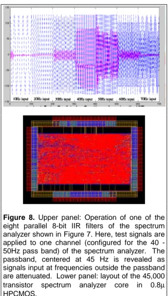
excessive number of taps and corresponding power dissipation. In contrast, IIR filter architectures have provided adequate resolution with limited word length. An example of the performance of a typical filter is shown in Figure 8. Here, a series of input signals at frequencies of 10 – 70 Hz were applied to the 8-bit data IIR filter with coefficients selected for a passband of 10 Hz width centered at 45 Hz. This device dissipates 3µW at 3V bias and at a 200Hz word rate.
7.
WINS Micropower Embedded Radio
WINS systems present novel requirements for low cost, low power, short range, and low bit rate RF communication. In contrast to previous emphasis in wireless networks for voice and data, distributed sensors and embedded microcontrollers raise these new requirements while relaxing the requirements on latency and throughput. The WINS RF modem becomes an embedded radio with a system that may be added to compact microdevices without significantly impacting cost, form factor, or power. However, in contrast to previously developed simple, low power RF modems, theFigure 8. Upper panel: Operation of one of the eight parallel 8-bit IIR filters of the spectrum analyzer shown in Figure 7. Here, test signals are applied to one channel (configured for the 40 -50Hz pass band) of the spectrum analyzer. The passband, centered at 45 Hz is revealed as signals input at frequencies outside the passband are attenuated. Lower panel: layout of the 45,000 transistor spectrum analyzer core in 0.8µ HPCMOS.
Figure 7. WINS micropower spectrum analyzer architecture. The sensor, ADC, buffer, filter bank, and decision systems operate continuously. Upon recognition of an event, microcontroller operation is initiated. sensor ADC control physical input signal buffer PSD computation comparator parallel IIR filter bank network interface
WINS device must fully support networking. In addition, the WINS radio should be compatible with compact packaging.
Communication and networking protocols for the embedded radio are now a topic of research. However, simulation and experimental verification in the field indicate that the embedded radio network must include spread spectrum signaling, channel coding, and time division multiple access (TDMA) network protocols. The operating bands for the embedded radio are most conveniently the unlicensed bands at 902-928 MHz and near 2.4 GHz. These bands provide a compromise between the power cost associated with high frequency operation and the penalty in antenna gain reduction with decreasing frequency for compact antennas. The prototype, operational, WINS networks are implemented with a self-assembling, multihop TDMA network protocol.
The WINS embedded radio development is directed to CMOS circuit technology to permit low cost fabrication along with the additional WINS components. Well known challenges accompany the development of RF systems in CMOS technology.[4] Of particular importance to the embedded radio are the problems associated with low transistor transconductance and the limitations of integrated passive RF components. In addition, WINS embedded radio design must address the peak current limitation of typical battery sources, of 1mA. This requires implementation of RF circuits that require one to two orders of magnitude lower peak power than conventional systems. Due to short range and low bit rate characteristics, however, the requirements for input noise figure may be relaxed. In addition, channel spacing for the embedded radio system may be increased relative to that of conventional RF modems, relaxing further the requirements on selectivity. Constraints on operating requirements must consider, however, resistance to interference by conventional spread spectrum radios occupying the same unlicensed bands.
The transceiver power dissipation in conventional RF modem systems is dominated, of course, by transmitter power. However, in the limit of low transmitter power (less than 1 – 3mW) for WINS, receiver system power dissipation equals or exceeds that of the transmitter. This is a direct result of the increased complexity of the receiver, the requirement for power dissipation in the first stage preamplifier (to obtain low noise operation) and the power dissipated by the voltage-controlled oscillator VCO. It is critical, therefore, to develop the methods for design of micropower CMOS active elements. These circuits must operate in the MOS subthreshold region at low transconductance. The VCO and mixer have been chosen as the first demonstrations of micropower, weak inversion mode RF systems. The VCO demonstrates the capability for high gain at high frequency and low power. In addition, the VCO demonstrates tunability and is a test for low noise
operation at low power. The weak inversion mixer demonstrates a test for linearity and distortion.
Conventional RF system design based on a combination of integrated and board level components, must employ interfaces between components that drive 50Ω resistive loads (since this is required for matching to off-chip transmission lines and components). However, by integrating active and passive components in a single package, impedance may be raised, dramatically reducing power dissipation. Impedance within component systems (for example the VCO) and between component systems, is controlled by the introduction of high-Q inductors at each node that balance the parasitic capacitance that would otherwise induce power dissipation. The introduction of high-Q inductors enable narrowband, high output impedance, weak inversion MOS circuits to be translated from low frequency to an equally narrow band at high frequency.
The micropower VCO has been demonstrated in both single ended (Colpitts) and differential cross-coupled pair architectures. In each case, the role of inductor properties on phase noise has been tested. First, as demonstrated by Leeson’s theory for LC oscillator phase noise power, Sφ, at frequency offset of δω away from the carrier at frequency ω with an input noise power, Snoise[5], and LC tank quality factor, Q, phase noise power is:
S
1
Q
2S
2 noise φ∝
δω
ω
Now, phase noise power, Snoise, at the transistor input, is dominated by “1/f” noise. Input referred thermal noise, in addition, increases with decreasing drain current and power dissipation due to the resulting decrease in transistor transconductance. Thus, conventional CMOS VCO circuits would provide degraded performance at the desired micropower level. However, for VCO systems operating with an LC resonator, having a complete circuit quality factor Q, the advantage in phase noise power is Q2. This phase noise advantage recovers the performance loss associated with power reduction. But, in addition, high Q resonators, providing voltage gain in the oscillator feedback loop, also allow for reduction in transistor transconductance. This also results in a reduction in power required to sustain oscillation.
The introduction of high-Q resonators in the embedded radio system presents the advantage of power reduction. However, this narrowband operation also creates a need for precision in passive component values and the need for tuning. Now, tunable elements are most conveniently based on varactor diodes implemented in the CMOS process. However, these diodes introduce loss. The tunability of micropower CMOS systems has been tested by implementation of several VCO systems to be discussed below.[1]
The inductors required for the embedded radio may be implemented in either on-chip elements or as passive off-chip components. Several studies have been directed to
on-chip LC circuits for CMOS RF systems.[4,6,7] Due to substrate and conductor losses, these inductors are limited to Q values of 3 – 5 at 1GHz. These successful circuit implementations are well-suited for broad band, high data rate, wireless systems. However, the embedded radio system requires narrow band operation and must exploit high Q value components.
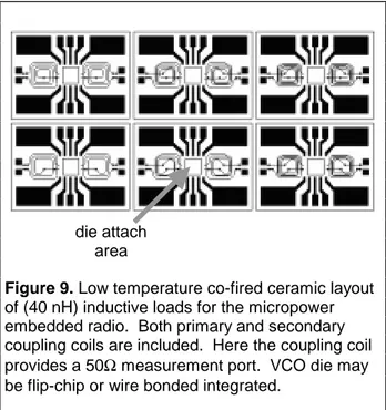
A series of high Q inductor systems have been investigated for embedded radio technology. Low temperature co-fired ceramic technology (LTCC) provides flexible device geometry and integration of flip-chip die attach on a substrate with embedded capacitor and inductor passives. The layout of typical inductor patterns in multilayer LTCC is shown in Figure 9. These inductor patterns provide a load for the oscillator and
also incorporate embedded coupling coils for external sensing of oscillator operation with conventional test equipment. This latter method is required to permit testing since the micropower RF components reported here may not directly supply the 50Ω load of standard instrumentation.
The LTCC substrate provides low loss passive components, but, in addition provides packaging support for integrated sensing, signal processing, and microcontroller devices. It is important to contrast the cost associated with on-chip inductors with that of inductors on the LTCC substrate. At 1GHz, the scale of integrated inductors implemented in CMOS technology dominates the area of a typical circuit die. However, the inductors implemented in the LTCC substrate require no die area at improved performance.[8]
Micropower oscillator performance was investigated using both single phase and differential oscillators
implemented in 0.8µ HPCMOS technology (see Figure 10). Layout of the oscillator transistor emphasizes an interdigitated structure to reduce loss in the transistor
itself.[1]
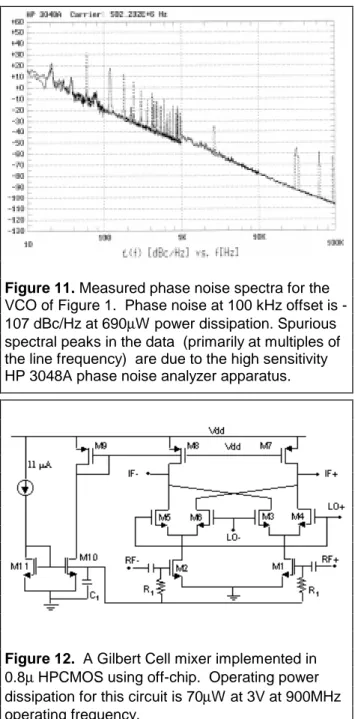
Characterization of the oscillator of Figure 10 demonstrate low phase noise (-107 dBc/Hz at 100kHz offset) and 10 percent tuning range (see Figure 11) Measurement of phase noise employs use of a weakly coupled coil (avoiding the need for 50Ω buffer stages) to sample the oscillation output to an HP 3048A phase noise measurement system. This phase noise compares favorably with the values measured for all CMOS VCO systems.[6] This tuning range is estimated to be adequate for operation of the embedded radio in the unlicensed bands and with the anticipated manufacturing tolerance of LTCC components.
The WINS embedded radio mixer design has been demonstrated for direct conversion operation with a series of circuit implementations. The Gilbert Cell mixer, implemented in weak inversion CMOS circuits is shown in Figure 12. This circuit draws only 22µA at 3V supply bias and shows an IF bandwidth of greater than 100kHz. Direct measurement of two-tone, third order intermodulation distortion and compression yield values of IP3 = -3dBm input power, and 1dB compression point of -12dBm effective input power. (These input power levels are effective input power: input signal power if the input signal voltage amplitude were applied to a 50Ω load). Voltage gain for the mixer was 12 dB. An example of mixer performance is shown in Figure 13.
The micropower mixer may operate at zero-IF (direct conversion to dc) or may be loaded with a high-Q inductor to provide high-IF frequency output without significant increase in operating power.
Figure 9. Low temperature co-fired ceramic layout of (40 nH) inductive loads for the micropower embedded radio. Both primary and secondary coupling coils are included. Here the coupling coil provides a 50Ω measurement port. VCO die may be flip-chip or wire bonded integrated.
M
2 M1 Rs L1 C1 Vdd Vtuning C2Figure 10. A Colpitts VCO implemented in 0.8µ HPCMOS using off-chip (40 nH) low loss
inductors. Both circuit and chip photo are shown. Operating power dissipation for this circuit is 300µW at 3V at 500MHz operating frequency.
die attach area
8.
WINS Summary
New architectures and circuits are required for wireless integrated network sensors. A series of interface, signal processing, and communication systems have been implemented in micropower CMOS circuits. Chopper input data converters for the WINS requirements of high stability and micropower have been demonstrated. Also, a micropower spectrum analyzer has been developed to enable low power operation of the entire WINS system. Finally, the lowest reported power dissipation CMOS RF oscillator and mixer circuits have been demonstrated. Recently, complete, prototype WINS networks have been demonstrated in defense,
factory automation, and condition based maintenance applications. These results reveal a wide range of new applications that require integrated, low cost, and compact WINS technology. Micropower WINS systems-on-a-chip will create a new, deeply embedded and densely distributed computing and sensing platform.
Acknowledgments
The authors would like to acknowledge valuable discussions with S. Molloy, R. Jain, and B. Razavi. We are also indebted to Scrantom Engineering Corporation for their development and fabrication of low temperature co-fired ceramic (LTCC) embedded passive RF components. This work was supported by the Defense Advanced Research Projects Agency, (DARPA) Electronics Technology Office and Tactical Technology Office.
References
[1] K. Bult, A. Burstein, D. Chang, M. Dong, M. Fielding, E. Kruglick, J. Ho, F. Lin, T. H. Lin, W. J. Kaiser, H. Marcy, R. Mukai, P. Nelson, F. Newberg, K. S. J. Pister, G. Pottie, H. Sanchez, O. M Stafsudd, K. B. Tan, C. M. Ward, S. Xue, J. Yao, “Low Power Systems for Wireless Microsensors”, 1996 International Symposium on Low Power Electronics and Design, Digest of Technical Papers, (1996), pp. 17-21
[2] E. Vittoz, Design of Analog-Digital VLSI Circuits for
Telecommunications & Signal Processing, Prentice Hall, New
York, 1994.
[3] M. J. Dong, G. Yung, and W. J. Kaiser, “Low Power Signal Processing Architectures for Network Microsensors”, 1997 International Symposium on Low Power Electronics and Design, Digest of Technical Papers (1997), pp. 173-177.
[4] A. A. Abidi, “Low-power radio-frequency ICs for portable communications”, Proceedings of the IEEE, 83, (1995), pp. 544-69.
[5] D. B. Leeson, “A simple model of feedback oscillator noise spectra”, Proc. IEEE, 54, (1966), pp. 329-330.
[6] J. Craninckx, M. S. J. Steyaert, “A 1.8-GHz low-phase-noise CMOS VCO using optimized hollow spiral inductors”
IEEE Journal of Solid-State Circuits, 32, (1997), pp.736-44.
[7] B. Razavi, “A Study of Phase Noise in CMOS Oscillators”, IEEE J. of Solid-State Circuits, 31, (1996), pp. 331-343.
[8] S. Vasudevan, A. Shaikh, “Microwave Charac-terization of Low Temperature Cofired Tape Ceramic System”,
Advancing Microelectronics, (1995), pp.16-25.
Figure 11. Measured phase noise spectra for the VCO of Figure 1. Phase noise at 100 kHz offset is -107 dBc/Hz at 690µW power dissipation. Spurious spectral peaks in the data (primarily at multiples of the line frequency) are due to the high sensitivity HP 3048A phase noise analyzer apparatus.
Figure 12. A Gilbert Cell mixer implemented in 0.8µ HPCMOS using off-chip. Operating power dissipation for this circuit is 70µW at 3V at 900MHz operating frequency.