19-1676; Rev 6; 3/15
General Description
The MAX6369–MAX6374 are pin-selectable watchdog timers that supervise microprocessor (µP) activity and signal when a system is operating improperly. During normal operation, the microprocessor should repeated-ly toggle the watchdog input (WDI) before the selected watchdog timeout period elapses to demonstrate that the system is processing code properly. If the µP does not provide a valid watchdog input transition before the timeout period expires, the supervisor asserts a watch-dog (WDO) output to signal that the system is not exe-cuting the desired instructions within the expected time frame. The watchdog output pulse can be used to reset the µP or interrupt the system to warn of processing errors.
The MAX6369–MAX6374 are flexible watchdog timer supervisors that can increase system reliability through notification of code execution errors. The family offers several pin-selectable watchdog timing options to match a wide range of system timing applications: • Watchdog startup delay: provides an initial delay
before the watchdog timer is started.
• Watchdog timeout period: normal operating watch-dog timeout period after the initial startup delay. • Watchdog output/timing options: open drain (100ms)
or push-pull (1ms).
The MAX6369–MAX6374 operate over a +2.5V to +5.5V supply range and are available in miniature 8-pin SOT23 packages.
Applications
Embedded Control Systems Industrial Controllers
Critical µP and Microcontroller (µC) Monitoring Automotive
Telecommunications Networking
Features
•
Precision Watchdog Timer for Critical µP Applications•
Pin-Selectable Watchdog Timeout Periods•
Pin-Selectable Watchdog Startup Delay Periods•
Ability to Change Watchdog Timing CharacteristicsWithout Power Cycling
•
Open-Drain or Push-Pull Pulsed Active-Low Watchdog Output•
Watchdog Timer Disable Feature•
+2.5V to +5.5V Operating Voltage•
8µA Low Supply Current•
No External Components Required•
Miniature 8-Pin SOT23 PackagePART OUTPUT WDO PULSE
WIDTH (ms) MINIMUM STARTUP DELAY MINIMUM WATCHDOG TIMEOUT
MAX6369 Open Drain 100 Selectable: 1ms to 60s S el ectab l e: 1ms to 60s MAX6370 Push-Pull 1 Selectable: 1ms to 60s S el ectab l e: 1ms to 60s MAX6371 Open Drain 100 60s S el ectab l e: 1ms to 60s MAX6372 Push-Pull 1 60s S el ectab l e: 1ms to 60s MAX6373 Open Drain 100 S el ectab l e: 200µs to 60s or fi r st ed g e S el ectab l e: 30µs to 10s MAX6374 Push-Pull 1 S el ectab l e: 200µs to 60s or fi r st ed g e S el ectab l e: 30µs to 10s
Selector Guide
PART TEMP RANGE PIN-PACKAGE TOP MARK MAX6369KA-T -40°C to +125°C 8 SOT23 AADC MAX6369KA/V-T -40°C to +125°C 8 SOT23 AEQV MAX6369KA/V+T -40°C to +125°C 8 SOT23 AEQVMAX6370KA-T -40°C to +125°C 8 SOT23 AADD
MAX6371KA-T -40°C to +125°C 8 SOT23 AADE
MAX6372KA-T -40°C to +125°C 8 SOT23 AADF
MAX6373KA-T -40°C to +125°C 8 SOT23 AADG
MAX6374KA-T -40°C to +125°C 8 SOT23 AADH
Ordering Information
Pin Configuration appears at end of data sheet.
Note:All devices are available in tape-and-reel only. Required order increment is 2,500 pieces.
/V denotes an automotive qualified part.
Devices are available in both leaded and lead-free packaging. Specify lead-free by replacing “-T” with “+T” when ordering.
Absolute Maximum Ratings
Electrical Characteristics
(VCC= +2.5V to +5.5V, SET_ = VCCor GND, TA= -40°C to +125°C, unless otherwise noted. Typical values are at TA= +25°C and VCC= +3V.) (Note 1)
Stresses beyond those listed under “Absolute Maximum Ratings” may cause permanent damage to the device. These are stress ratings only, and functional operation of the device at these or any other conditions beyond those indicated in the operational sections of the specifications is not implied. Exposure to absolute maximum rating conditions for extended periods may affect device reliability.
Terminal Voltage (with respect to GND)
VCC...-0.3V to +6V WDI...-0.3V to +6V
WDO(Open Drain: MAX6369/71/73) ...-0.3V to +6V
WDO(Push-Pull: MAX6370/72/74 ...-0.3V to (VCC+ 0.3V) SET0, SET1, SET2 ...-0.3V to (VCC+ 0.3V) Maximum Current, Any Pin (input/output)...20mA
Continuous Power Dissipation (TA= +70°C)
8-Pin SOT23 (derate 8.75mW/°C above +70°C)...700mW Operating Temperature Range ...-40°C to +125°C Storage Temperature Range ...-65°C to +150°C Junction Temperature ...+150°C VCCRise or Fall Rate...0.05V/µs Lead Temperature (soldering, 10s) ...+300°C Soldering Temperature (reflow)
Lead(Pb)-free...+260°C Containing Lead (Pb)...+240°C
PARAMETER SYMBOL CONDITIONS MIN TYP MAX UNITS
Operating Voltage Range VCC 2.5 5.5 V
TA = -40°C to +85°C 8 20
Supply Current ICC No load
TA = -40°C to +125°C 10 22
µA
Input High Voltage VIH WDI, SET0, SET1, SET2 0.8 × VCC V
VCC≥ 3.3V, TA = -40°C to +85°C 0.8 VCC≥ 3.3V, TA = -40°C to +125°C 0.6 VCC≥ 2.5V, TA = -40°C to +85°C 0.6
Input Low Voltage VIL WDI, SET0,
SET1, SET2
VCC≥ 2.5V,
TA = -40°C to +125°C 0.4
V
Logic Input Current (Note 2) VWDI or VSET_ = 0V or VCC 0 ±10 nA
ISINK = 1.2mA, VCC > 2.7V, watchdog
output asserted 0.3 V
WDO Output Low
Voltage VOL ISINK = 6mA, VCC > 4.5V, watchdog
output asserted 0.4 V
WDO Leakage Current ILKG VWDO = 0 to +5.5V, output deasserted,
MAX6369/MAX6371/MAX6373 1 µA
ISOURCE = 500µA, VCC > 2.7V, watchdog
output deasserted 0.8 × VCC
WDO Output High
Voltage VOH ISOURCE = 800µA, VCC > 4.5V, watchdog
output deasserted VCC - 1.5
Maxim Integrated | 3 www.maximintegrated.com
Electrical Characteristics (continued)
(VCC= +2.5V to +5.5V, SET_ = VCCor GND, TA= -40°C to +125°C, unless otherwise noted. Typical values are at TA= +25°C and VCC= +3V.) (Note 1)
PARAMETER SYMBOL CONDITIONS MIN TYP MAX UNITS
MAX6369/MAX6370
VSET2 = 0V, VSET1 = 0V, VSET0 = 0V 1 3
VSET2 = 0V, VSET1 = 0,V SET0 = VCC 10 30
VSET2 = 0V, SET1 = VCC, VSET0 = 0V 30 90
ms
VSET2 = 0V, SET1 = VCC, SET0 = VCC Watchdog Disabled
SET2 = VCC, VSET1 = 0V, VSET0 = 0V 100 300 ms
SET2 = VCC, VSET1 = 0V, SET0 = VCC 1 3
SET2 = VCC, SET1 = VCC, VSET0 = 0V 10 30
Startup Delay Period tDELAY
SET2 = VCC, SET1 = VCC, SET0 = VCC 60 180
s
VSET2 = 0V, VSET1 = 0V, VSET0 = 0V 1 3
VSET2 = 0V, VSET1 = 0V, SET0 = VCC 10 30
VSET2 = 0V, SET1 = VCC, VSET0 = 0V 30 90
ms
VSET2 = 0V, SET1 = VCC, SET0 = VCC Watchdog Disabled
SET2 = VCC, VSET1 = 0V, VSET0 = 0V 100 300 ms
SET2 = VCC, VSET1 = 0V, SET0 = VCC 1 3
SET2 = VCC, SET1 = VCC, VSET0 = 0V 10 30
Watchdog Timeout
Period tWD
SET2 = VCC, SET1 = VCC, SET0 = VCC 60 180
s
MAX6371/MAX6372
VSET2 = 0V, SET1 = VCC, SET0 = VCC Watchdog Disabled
Startup Delay Period tDELAY
All other SET_ conditions 60 180 s VSET2 = 0V, VSET1 = 0V, VSET0 = 0V 1 3
VSET2 = 0V, VSET1 = 0V, SET0 = VCC 3 9
VSET2 = 0V, SET1 = VCC, VSET0 = 0V 10 30
ms
VSET2 = 0V, SET1 = VCC, SET0 = VCC Watchdog Disabled SET2 = VCC, VSET1 = 0V, VSET0 = 0V 100 300
SET2 = VCC, VSET1 = 0V, SET0 = VCC 300 900
ms
SET2 = VCC, SET1 = VCC, VSET0 = 0V 3 9
Watchdog Time-Out
Period tWD
SET2 = VCC, SET1 = VCC, SET0 = VCC 60 180
s
MAX6373/MAX6374
VSET2 = 0V, VSET1 = 0V, VSET0 = 0V 3 9 ms
VSET2 = 0V, VSET1 = 0V, SET0 = VCC 3 9
VSET2 = 0V, SET1 = VCC, VSET0 = 0V 60 180
s SET2 = 0V, SET1 = VCC, SET0 = VCC Watchdog Disabled
SET2 = VCC, VSET1 = 0V, VSET0 = 0V 200 600 µs
SET2 = VCC, VSET1 = 0V, SET0 = VCC First Edge (Note 3)
SET2 = VCC, SET1 = VCC, VSET0 = 0V First Edge (Note 3)
Startup Delay Period tDELAY
4 6 10 8 12 14 -40 -15 10 35 60 85 SUPPLY CURRENT vs. TEMPERATURE MAX6369/74-01 TEMPERATURE (°C) SUPPLY CURRENT ( μ A) VCC = +5.5V VCC = +2.5V
Typical Operating Characteristics
(Circuit of Figure 1, TA= +25°C, unless otherwise noted.)0.997 0.999 0.998 1.001 1.000 1.002 1.003 -40 -15 10 35 60 85
WATCHDOG TIMEOUT PERIOD vs. TEMPERATURE
MAX6369/74-02
TEMPERATURE (°C)
NORMALIZED WATCHDOG TIMEOUT PERIOD
Electrical Characteristics (continued)
(VCC= +2.5V to +5.5V, SET_ = VCCor GND, TA= -40°C to +125°C, unless otherwise noted. Typical values are at TA= +25°C and VCC= +3V.) (Note 1)
PARAMETER SYMBOL CONDITIONS MIN TYP MAX UNITS
VSET2 = 0V, VSET1 = 0V, VSET0 = 0V 3 9 ms
VSET2 = 0V, VSET1 = 0V, SET0 = VCC 3 9
VSET2 = 0V, SET1 = VCC, VSET0 = 0V 1 3
s
VSET2 = 0V, SET1 = VCC, SET0 = VCC Watchdog Disabled
SET2 = VCC, VSET1 = 0V, VSET0 = 0V 30 90 µs
SET2 = VCC, VSET1 = 0V, SET0 = VCC 1 3
SET2 = VCC, SET1 = VCC, VSET0 = 0V 10 30
Watchdog Timeout
Period tWD
SET2 = VCC, SET1 = VCC, SET0 = VCC 10 30
s
Watchd og Inp ut P ul se Wi d th
( N ote 2) tWDI After WDO deasserted 100 ns MAX6369/MAX6371/MAX6373 100 300 ms Watchdog Output Pulse Width tWDO
MAX6370/MAX6372/MAX6374 1 3 ms Internal Setup Time
(Note 4) tSETUP After WDO deasserted 300 µs Note 1:Production tested at TA= +25°C. Guaranteed by design over temperature limits.
Note 2:Guaranteed by design.
Note 3:In this setting the watchdog timer is inactive and startup delay ends when WDI sees its first level transition. See the Selecting Device Timing section for more information.
Maxim Integrated | 5 www.maximintegrated.com
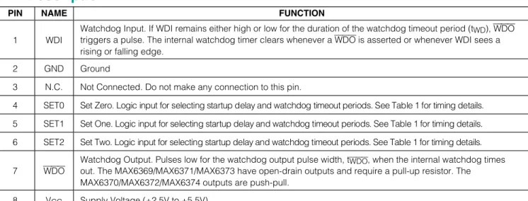
PIN NAME FUNCTION
1 WDI
Watchdog Input. If WDI remains either high or low for the duration of the watchdog timeout period (tWD), WDO
triggers a pulse. The internal watchdog timer clears whenever a WDO is asserted or whenever WDI sees a rising or falling edge.
2 GND Ground
3 N.C. Not Connected. Do not make any connection to this pin.
4 SET0 S et Z er o. Log i c i np ut for sel ecti ng star tup d el ay and w atchd og ti m eout p er i od s. S ee Tab l e 1 for ti m i ng d etai l s. 5 SET1 S et One. Log i c i np ut for sel ecti ng star tup d el ay and w atchd og ti m eout p er i od s. S ee Tab l e 1 for ti m i ng d etai l s. 6 SET2 S et Tw o. Log i c i np ut for sel ecti ng star tup d el ay and w atchd og ti m eout p er i od s. S ee Tab l e 1 for ti m i ng d etai l s.
7 WDO
Watchdog Output. Pulses low for the watchdog output pulse width, tWDO, when the internal watchdog times out. The MAX6369/MAX6371/MAX6373 have open-drain outputs and require a pull-up resistor. The MAX6370/MAX6372/MAX6374 outputs are push-pull.
8 VCC Supply Voltage (+2.5V to +5.5V)
Table 1. Minimum Timeout Settings
Pin Description
Detailed Description
The MAX6369–MAX6374 are flexible watchdog circuits for monitoring µP activity. During normal operation, the internal timer is cleared each time the µP toggles the WDI with a valid logic transition (low to high or high to low) within the selected timeout period (tWD). The WDO remains high as long as the input is strobed within the selected timeout period. If the input is not strobed before the timeout period expires, the watchdog output is asserted low for the watchdog output pulse width (tWDO). The device type and the state of the three logic control pins (SET0, SET1, and SET2) determine watch-dog timing characteristics. The three basic timing varia-tions for the watchdog startup delay and the normal
watchdog timeout period are summarized below (see Table 1 for the timeout characteristics for all devices in the family):
• Watchdog Startup Delay:
Provides an initial delay before the watchdog timer is started.
Allows time for the µP system to power up and initial-ize before assuming responsibility for normal watch-dog timer updates.
Includes several fixed or pin-selectable startup delay options from 200µs to 60s, and an option to wait for the first watchdog input transition before starting the watchdog timer.
LOGIC INPUTS MAX6369/MAX6370 MAX6371/MAX6372 MAX6373/MAX6374
SET2 SET1 SET0 tDELAY, tWD tDELAY = 60s, tWD tDELAY tWD
0 0 0 1ms 1ms 3ms 3ms
0 0 1 10ms 3ms 3s 3s
0 1 0 30ms 10ms 60s 1s
0 1 1 Disabled Disabled Disabled Disabled
1 0 0 100ms 100ms 200μs 30μs
1 0 1 1s 300ms First Edge 1s
1 1 0 10s 3s First Edge 10s
• Watchdog Timeout Period:
Normal operating watchdog timeout period after the initial startup delay.
A watchdog output pulse is asserted if a valid watch-dog input transition is not received before the timeout period elapses.
Eight pin-selectable timeout period options for each device, from 30µs to 60s.
Pin-selectable watchdog timer disable feature.
• Watchdog Output/Timing Options:
Open drain, active low with 100ms minimum watch-dog output pulse (MAX6369/MAX6371/MAX6373). Push-pull, active low with 1ms minimum watchdog output pulse (MAX6370/MAX6372/MAX6374).
Each device has a watchdog startup delay that is initi-ated when the supervisor is first powered or after the user modifies any of the logic control set inputs. The watchdog timer does not begin to count down until the
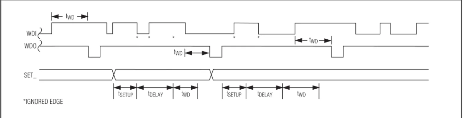
VCC WDI WDO tSETUP tDELAY tWD tWD tWD tWDO A B C D E F G
TRANSITIONS ON WDI IGNORED DURING SETUP DELAY. TRANSITION(S) ON WDI IGNORED DURING STARTUP DELAY PERIOD. WATCHDOG TIMER STARTS AFTER STARTUP DELAY AND WDO IS DEASSERTED. TRANSITION OCCURS BEFORE WATCHDOG TIMEOUT PERIOD. WATCHDOG TIMER CLEARS AND STARTS TIMER AGAIN.
WATCHDOG TIMES OUT, WDO ASSERTS.
TRANSITIONS ON WDI IGNORED WHEN WDO ASSERTED. WATCHDOG TIMER STARTS AFTER WDO DEASSERTS.
A
A B C D E F G E
Figure 2. Watchdog Timing
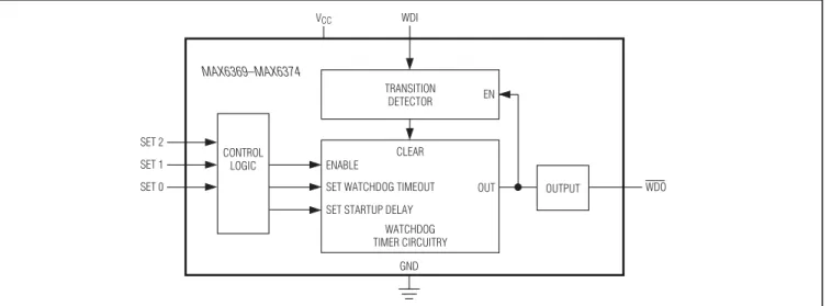
WATCHDOG TIMER CIRCUITRY
TRANSITION DETECTOR
ENABLE
SET WATCHDOG TIMEOUT SET STARTUP DELAY
MAX6369–MAX6374 EN CONTROL LOGIC SET 2 SET 1 SET 0 VCC GND CLEAR WDO OUT WDI OUTPUT
Maxim Integrated | 7 www.maximintegrated.com
completion of the startup delay period, and no watch-dog output pulses are asserted during the startup delay. When the startup delay expires, the watchdog begins counting its normal watchdog timeout period and waiting for WDI transitions. The startup delay allows time for the µP system to power up and fully ini-tialize before assuming responsibility for the normal watchdog timer updates. Startup delay periods vary between the different devices and may be altered by the logic control set pins. To ensure that the system generates no undesired watchdog outputs, the routine watchdog input transitions should begin before the selected minimum startup delay period has expired. The normal watchdog timeout period countdown is initi-ated when the startup delay is complete. If a valid logic transition is not recognized at WDI before the watchdog timeout period has expired, the supervisor asserts a watchdog output. Watchdog timeout periods vary between the different devices and may be altered by the logic control set pins. To ensure that the system generates no undesired watchdog outputs, the watch-dog input transitions should occur before the selected minimum watchdog timeout period has expired.
The startup delay and the watchdog timeout period are determined by the states of the SET0, SET1, and SET2 pins, and by the particular device within the family. For the MAX6369 and MAX6370, the startup delay is equal to the watchdog timeout period. The startup and watchdog timeout periods are pin selectable from 1ms to 60s (minimum).
For the MAX6371 and MAX6372, the startup delay is fixed at 60s and the watchdog timeout period is pin selectable from 1ms to 60s (minimum).
The MAX6373/MAX6374 provide two timing variations for the startup delay and normal watchdog timeout. Five of the pin-selectable modes provide startup delays from 200µs to 60s minimum, and watchdog timeout
delays from 3ms to 10s minimum. Two of the selectable modes do not initiate the watchdog timer until the device receives its first valid watchdog input transition (there is no fixed period by which the first input must be received). These two extended startup delay modes are useful for applications requiring more than 60s for system initialization.
All the MAX6369–MAX6374 devices may be disabled with the proper logic control pin setting (Table 1).
Applications Information
Input Signal Considerations
Watchdog timing is measured from the last WDI rising or falling edge associated with a pulse of at least 100ns in width. WDI transitions are ignored when WDO is asserted, and during the startup delay period (Figure 2). Watchdog input transitions are also ignored for a setup period, tSETUP, of up to 300µs after power-up or a setting change (Figure 3).
Selecting Device Timing
SET2, SET1, and SET0 program the startup delay and watchdog timeout periods (Table 1). Timeout settings can be hard wired, or they can be controlled with logic gates and modified during operation. To ensure smooth transitions, the system should strobe WDI immediately before the timing settings are changed. This minimizes the risk of initializing a setting change too late in the timer countdown period and generating undesired watchdog outputs. After changing the timing settings,
two outcomes are possible based on WDO. If the
change is made while WDOis asserted, the previous setting is allowed to finish, the characteristics of the new setting are assumed, and the new startup phase is entered after a 300µs setup time (tSETUP) elapses. If the change is made while WDO is not asserted, the new setting is initiated immediately, and the new start-up phase is entered after the 300µs setstart-up time elapses.
tWD
tWD
tWD
tSETUP tDELAY tWD tSETUP tDELAY tWD
* * * * *
*IGNORED EDGE WDI WDO
SET_
Selecting 011 (SET2 = 0, SET1 = 1, SET0 = 1) disables the watchdog timer function on all devices in the family. Operation can be reenabled without powering down by changing the set inputs to the new desired setting. The device assumes the new selected timing characteris-tics and enter the startup phase after the 300µs setup time elapses (Figure 3). WDO is high when the watch-dog timer is disabled.
The MAX6373/MAX6374 offer a first-edge feature. In first-edge mode (settings 101 or 110, Table 1), the internal timer does not control the startup delay period. Instead, startup terminates when WDI sees a transition. If changing to first-edge mode while the device is oper-ating, disable mode must be entered first. It is then safe to select first-edge mode. Entering disable mode first ensures the output is unasserted when selecting first-edge mode and removes the danger of WDI being masked out.
Output
The MAX6369/MAX6371/MAX6373 have an active-low, open-drain output that provides a watchdog output pulse of 100ms. This output structure sinks current when WDO is asserted. Connect a pullup resistor from WDOto any supply voltage up to +5.5V.
Select a resistor value large enough to register a logic low (see Electrical Characteristics), and small enough to register a logic high while supplying all input current and leakage paths connected to the WDOline. A 10kΩ pullup is sufficient in most applications. The MAX6370/ MAX6372/MAX6374 have push-pull outputs that pro-vide an active-low watchdog output pulse of 1ms.
When WDO deasserts, timing begins again at the
beginning of the watchdog timeout period (Figure 2).
Usage in Noisy Environments
If using the watchdog timer in an electrically noisy envi-ronment, a bypass capacitor of 0.1µF should be con-nected between VCCand GND as close to the device as possible, and no further away than 0.2 inches.
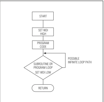
Watchdog Software
Considerations
To help the watchdog timer monitor software execution more closely, set and reset the watchdog input at differ-ent points in the program, rather than pulsing the watch-dog input high-low-high or low-high-low. This technique avoids a stuck loop, in which the watchdog timer would continue to be reset inside the loop, keeping the watch-dog from timing out. Figure 4 shows an example of a flow diagram where the I/O driving the watchdog input is set high at the beginning of the program, set low at the end of every subroutine or loop, then set high again when the program returns to the beginning. If the pro-gram should hang in any subroutine, the problem would be quickly corrected, since the I/O is continually set low and the watchdog timer is allowed to time out, causing WDOto pulse. START SET WDI HIGH PROGRAM CODE SUBROUTINE OR PROGRAM LOOP SET WDI LOW
RETURN
POSSIBLE INFINITE LOOP PATH
Maxim Integrated | 9 www.maximintegrated.com
Chip Information
TRANSISTOR COUNT: 1500 PROCESS: BiCMOS SET2 SET1 SET0 1 2 8 7 VCC WDO GND N.C. WDI SOT23 TOP VIEW 3 4 6 5 MAX6369 MAX6370 MAX6371 MAX6372 MAX6373 MAX6374Pin Configuration
PACKAGE TYPE PACKAGE CODE OUTLINE NO. LAND PATTERN NO. 8 SOT23 K8SN-1 21-0078 90-0176Package Information
For the latest package outline information and land patterns (foot-prints), go to www.maximintegrated.com/packages. Note that a “+”, “#”, or “-” in the package code indicates RoHS status only. Package drawings may show a different suffix character, but the drawing pertains to the package regardless of RoHS status.
Maxim Integrated cannot assume responsibility for use of any circuitry other than circuitry entirely embodied in a Maxim Integrated product. No circuit patent licenses are implied. Maxim Integrated reserves the right to change the circuitry and specifications without notice at any time. The parametric values (min and max limits) shown in the Electrical Characteristics table are guaranteed. Other parametric values quoted in this data sheet are provided for guidance.
For pricing, delivery, and ordering information, please contact Maxim Direct at 1-888-629-4642, or visit Maxim Integrated’s website at www.maximintegrated.com.
Revision History
REVISION NUMBER REVISION DATE DESCRIPTION PAGES CHANGED 0 4/00 Initial release —1 7/00 Removed future product asterisk for MAX6370. 1 2 2/03 Corrected limits in Electrical Characteristics. 4 3 12/05 Added lead-free information to Ordering Information. 1 4 6/10 Revised the CharacteristicsOrdering Information, and the Selecting Device Timing, Absolute Maximum Ratings section. , Electrical 1, 2, 8 5 1/11 Updated the top mark information in the Ordering Information section. 1 6 3/15 Deleted minimum value for Internal Setup Time in and changed units from ms to µs Electrical Characteristics 4