c
ENERGY EFFICIENT CORE DESIGNS FOR UPCOMING PROCESS TECHNOLOGIES
BY
BHARGAVA REDDY GOPIREDDY
DISSERTATION
Submitted in partial fulfillment of the requirements for the degree of Doctor of Philosophy in Computer Science
in the Graduate College of the
University of Illinois at Urbana-Champaign, 2019
Urbana, Illinois Doctoral Committee:
Professor Josep Torrellas, Chair Professor Wen-Mei Hwu
Professor Nam Sung Kim Professor Christopher Fletcher Dr. Asit Mishra, Nvidia
ABSTRACT
Energy efficiency has been a first order constraint in the design of micro processors for the last decade. As Moore’s law sunsets, new technologies are being actively explored to extend the march in increasing the computational power and efficiency. It is essential for computer architects to understand the opportunities and challenges in utilizing the upcoming process technology trends in order to design the most efficient processors. In this work, we consider three process technology trends and propose core designs that are best suited for each of the technologies. The process technologies are expected to be viable over a span of timelines.
We first consider the most popular method currently available to improve the energy ef-ficiency, i.e. by lowering the operating voltage. We make key observations regarding the limiting factors in scaling down the operating voltage for general purpose high performance processors. Later, we propose our novel core design, ScalCore, one that can work in high performance mode at nominal Vdd, and in a very energy-efficient mode at low Vdd. The re-sulting core design can operate at much lower voltages providing higher parallel performance while consuming lower energy.
While loweringVdd improves the energy efficiency, CMOS devices are fundamentally lim-ited in their low voltage operation. Therefore, we next consider an upcoming device technol-ogy – Tunneling Field-Effect Transistors (TFETs), that is expected to supplement CMOS device technology in the near future. TFETs can attain much higher energy efficiency than CMOS at low voltages. However, their performance saturates at high voltages and, there-fore, cannot entirely replace CMOS when high performance is needed. Ideally, we desire a core that is as energy-efficient as TFET and provides as much performance as CMOS. To reach this goal, we characterize the TFET device behavior for core design and judiciously integrate TFET units, CMOS units in a single core. The resulting core, called HetCore, can provide very high energy efficiency while limiting the slowdown when compared to a CMOS core.
Finally, we analyze Monolithic 3D (M3D) integration technology that is widely considered to be the only way to integrate more transistors on a chip. We present the first analysis of the architectural implications of using M3D for core design and show how to partition the core across different layers. We also address one of the key challenges in realizing the technology, namely, the top layer performance degradation. We propose a critical path based partitioning for logic stages and asymmetric bit/port partitioning for storage stages. The result is a core that performs nearly as well as a core without any top layer slowdown. When
compared to a 2D baseline design, an M3D core not only provides much higher performance, it also reduces the energy consumption at the same time.
In summary, this thesis addresses one of the fundamental challenges in computer architec-ture – overcoming the fact that CMOS is not scaling anymore. As we increase the computing power on a single chip, our ability to power the entire chip keeps decreasing. This thesis proposes three solutions aimed at solving this problem over different timelines. Across all our solutions, we improve energy efficiency without compromising the performance of the core. As a result, we are able to operate twice as many cores with in the same power budget as regular cores, significantly alleviating the problem of dark silicon.
ACKNOWLEDGMENTS
I would like express my deep gratitude to a number of people who have helped me in reaching this milestone. Firstly, I would like to express my sincere gratitude to my advisor Professor Josep Torrellas, for his help along the way. It was a wonderful experience working with him and I cannot imagine having a better advisor and mentor for my Ph.D. His hard work, motivation and dedication are inspirational to every graduate student. I hope to emulate his drive, patience and unwavering commitment going forward.
Besides my advisor, I would like thank the rest of my committee: Professor Christopher Fletcher, Professor Wen-Mei Hwu, Professor Nam Sung Kim, and Dr. Asit Mishra for their helpful comments and encouragement. In particular, I wish to thank Professor Christopher Fletcher, whom I had a chance to work with towards the later part of my Ph.D. The stim-ulating discussions with him on various projects were particularly enjoyable. Next, I would also like thank Dr. Asit Mishra for his help and guidance on my research work as well as during my internship.
Our iacoma research group is full of wonderful, talented and kind students. I would like thank all my fellow lab mates for the stimulating discussions, for the constant encouragement, for enduring the stress together before the deadlines, and for all the fun we have had in the years here. I would like to thank Dimitris and Mengjia in particular for giving me a chance to work with them on exciting projects such as Cloudburst, Sharp and Microscope etc., and for being a constant source of motivation. I would also like to mention my lab mates Raghavendra, Tom and Jiho for sharing the Ph.D. journey with me and for being partners in mutual guidance, learning and discovery. Next, I would like to thank Aditya Agrawal and Amin Ansari, for their advice in the early phase of my research. In addition, I am thankful to all my other collaborators and/or lab mates Yasser, Tanmay, Azin, Antonio, Apostolos, and Serif for their helpful feedback over the years.
I wish to express my special thanks to the various staff in the Computer Science department who helped me along the way. I am grateful to Sherry Unkraut, Madeleine Garvey for all their help with the administrative tasks and for sharing the tips that made my life easier. Similarly, I wish to thank Kara McGregor, Kathy Ann Runck, Mary Beth Kelley, Viveka Kudaligama and Maggie Metzger Chappell for cheerfully guiding me through the processes. I am lucky to meet a great group of people in Champaign-Urbana who enriched my life significantly and made my stay memorable. In particular, I would like mention our lunch group that consisted of Prasanna, Aditya, Shaileshh and Kaushik. The lunch meet up was
a source of joy and relief that I genuinely looked forward to every day. A special thanks to Sridhar, Nandu and Virajith whose friendship I will always cherish. Finally, I have to mention my friends Ashutosh, Kalyan, Kartik, Kavya, Ketan, Khetan, Madan, Praveen, Sangeetha, Sashi, Shreya and Swetha who made my stay here fun and enjoyable.
Most importantly, I convey my heartful thanks to my wife Pavithra. I am glad to have met you here in Urbana-Champaign during my doctoral study. You have been a great source of motivation and inspiration. You were always there for me; in the times of joy as well as stress. Thank you Pavi. Finally, I would like to express my gratitude and thanks to my parents and my sister for inspiring me, for providing me a great platform to succeed, and for constantly encouraging me in all my endeavors. I proudly dedicate this thesis to you.
TABLE OF CONTENTS
LIST OF TABLES . . . ix
LIST OF FIGURES . . . x
CHAPTER 1 INTRODUCTION . . . 1
1.1 Summary of the Work . . . 2
1.2 Challenges and Our Contributions . . . 3
1.3 Long Term Impact . . . 5
1.4 Thesis Organization . . . 6
CHAPTER 2 SCALCORE: DESIGNING A CORE FOR VOLTAGE SCALABILITY 8 2.1 Introduction . . . 8 2.2 Motivation . . . 9 2.3 ScalCore Concept . . . 12 2.4 ScalCore Design . . . 18 2.5 Implementation Considerations . . . 23 2.6 Implications on Applications . . . 26 2.7 Evaluation Methodology . . . 27 2.8 Evaluation . . . 30 2.9 Summary . . . 35
CHAPTER 3 HETCORE: TFET-CMOS HETERO-DEVICE ARCHITECTURE FOR CPUS AND GPUS . . . 36
3.1 Introduction . . . 36 3.2 Background . . . 37 3.3 Architecture Implications . . . 40 3.4 HetCore Architecture . . . 45 3.5 Implementation Considerations . . . 51 3.6 Evaluation Setup . . . 53 3.7 Evaluation . . . 55 3.8 Summary . . . 62
CHAPTER 4 DESIGNING VERTICAL PROCESSORS IN MONOLITHIC3D: OPPORTUNITIES, CHALLENGES AND TRADEOFFS . . . 63
4.1 Introduction . . . 63
4.2 3D Monolithic Integration . . . 64
4.3 M3D Core Design . . . 71
4.4 Hetero Layer M3D Design . . . 77
4.5 Architectures Enabled by M3D . . . 82
4.7 Evaluation . . . 87
4.8 Summary . . . 91
CHAPTER 5 RELATED WORK . . . 93
5.1 Building Voltage Scalable Cores . . . 93
5.2 Building Cores using CMOS-TFET Devices . . . 93
5.3 3D Partitioning of Cores . . . 94
CHAPTER 6 CONCLUSION . . . 96
LIST OF TABLES
2.1 Enhancements considered for different structures. . . 18
2.2 Microarchitectural changes in ScalCore. . . 22
2.3 Summary of ScalCore overheads. . . 24
2.4 Comparing Intel Claremont to ScalCore. . . 25
2.5 Parameters of the simulated architecture for the evaluation of ScalCore. . . . 27
2.6 HPMode and EEMode design points. . . 28
2.7 Configurations explored in low Vdd. . . 28
3.1 Characteristics of CMOS and TFET technologies at 15nm, using data from [1, 2]. . . 40
3.2 Design modifications for HetCore. . . 51
3.3 Parameters of the simulated architecture for the evaluation of HetCore. . . . 53
3.4 CPU and GPU configurations evaluated. . . 54
4.1 Area overhead of an MIV and a TSV compared to a 32-bit adder and a 32-bit SRAM cell at 15nm. . . 66
4.2 Physical dimensions and electrical characteristics of typical copper MIV and TSVs [3, 4, 5]. . . 67
4.3 Percentage reduction in access latency, access energy, and area footprint through bit partitioning. . . 74
4.4 Percentage reduction in access latency, access energy, and area footprint through word partitioning. . . 75
4.5 Percentage reduction in access latency, access energy, and area footprint through port partitioning. . . 75
4.6 Best partition for each structure and percentage reduction in latency, en-ergy and area footprint. . . 76
4.7 Partitioning techniques for a hetero-layer M3D core. . . 77
4.8 Percentage reduction in access latency, access energy, and area footprint with our hetero-layer partitioning compared to a 2D layout. . . 79
4.9 Parameters of the simulated architecture for the evaluation of an M3D Core. 84 4.10 Thermal modeling parameters for M3D & TSV3D. . . 85
LIST OF FIGURES
2.1 Effect of the number of fins in the FinFETs of the 8T cell on energy
consumption for differentVdds. . . 12
2.2 Increase in delay for logic and storage structures in the pipeline as we decreaseVdd. . . 13
2.3 Vdd-f curves for logic and storage structures. . . 14
2.4 Pipeline of an out-of-order processor with the main storage structures. . . 15
2.5 Datapath changes in ScalCore: Fusing pipeline stages using a flow-through latch. The shaded components are disabled. . . 19
2.6 Datapath changes in ScalCore: Increasing the size with transmission gates. The shaded components are disabled. . . 20
2.7 ScalCore pipeline with dual voltage rails. . . 22
2.8 Level converter for up-conversion. . . 23
2.9 Configurations for a fixed power. . . 30
2.10 Execution time of different designs with the same power, normalized to 16-Pipe2Vdd. . . 31
2.11 Energy consumption of different designs with the same power, normalized to16-Pipe2Vdd. . . 31
2.12 Energy-delay product of different designs with the same power normalized to16-Pipe2Vdd. . . 32
2.13 Execution time of different designs with 16 cores normalized to Pipe2Vdd. . . 33
2.14 Energy-delay product of different designs with 16 cores normalized toPipe2Vdd. 33 2.15 Dynamically reconfiguring ScalCore. . . 34
3.1 ID-VG characteristics of N-HetJTFET and N-MOSFET based on data from Intel [6]. . . 39
3.2 Total power consumption of a Si-CMOS ALU and a HetJTFET ALU with varying activity factors. . . 42
3.3 Vdd-freq. curves for Si-CMOS and HetJTFET. . . 44
3.4 TFET-based units selected for the BaseHet design. . . 46
3.5 Schematic design of anAsymmetric Cache. . . 48
3.6 HetCore dual voltage rail design. . . 51
3.7 Execution time of different CPU designs, normalized to BaseCMOS. . . 56
3.8 Energy consumption of different CPU designs, normalized to BaseCMOS. . . 56
3.9 ED2 of different CPU designs, normalized to BaseCMOS. . . . 56
3.10 Execution time of different GPU designs, normalized to BaseCMOS. . . 58
3.11 Energy consumption of different GPU designs, normalized to BaseCMOS. . . 58
3.12 ED2 of different GPU designs, normalized to BaseCMOS. . . . . 59
3.13 Sensitivity analysis of HetCore CPU designs. . . 60
3.14 Impact of DVFS and process variation on the energy consumed by BaseC-MOS and AdvHet. . . 62
4.1 M3D integration of two layers. . . 65
4.2 Relative area of an FO1 inverter, an MIV, an SRAM bitcell, and a TSV. . . 66
4.3 Partitioning an SRAM array using bit partitioning (a), word partitioning (b), and port partitioning (c). . . 69
4.4 Two cores sharing the L2 and the router stop. . . 72
4.5 Basic structure of an SRAM array. . . 73
4.6 ALU with shaded critical path blocks. . . 78
4.7 Speedup of different M3D designs over the Base (2D). . . 88
4.8 Energy of different M3D designs, normalized to Base (2D). . . 88
4.9 Peak Temperature of different CPU designs. . . 89
4.10 Speedup of MultiCore CPU designs, over the Base (2D). . . 91
CHAPTER 1: INTRODUCTION
In pursuit of higher performance, computer architects have embraced multi-core designs to work around the power wall that halted the rapid progress in increasing single core frequency. Additional transistors available on a chip at smaller process technology nodes are now employed to increase the number of cores on a single chip. This proved to be a good alternative that could provide higher performance at the same operating frequency, for applications that are inherently parallel. However, the number of cores that can run at their highest operating frequency in a large many-core chip is limited by the amount of heat that can be dissipated by the chip. Therefore, only a limited subset of cores can be operated at a time, resulting in dark silicon [7]. Researchers have been exploring several approaches to utilize the additional transistors available on newer process technologies without running into the problem of dark silicon.
One of the widely considered solutions to this problem involves operating the processor cores at a lower voltage and frequency. As a result, the power consumption of each core is reduced and more cores can be turned on within the same power budget. Such a design is also advantageous, as the energy efficiency is higher at lower voltages, i.e. energy consumed per operation is lower at lower voltages. In particular, it is well known that a near-threshold voltage operation provides the highest energy efficiency [8]. However, at these low voltages, the single threaded performance is poor. As applications tend to have alternating serial and parallel code sections, ideally, we need a design that not only operates all the cores available during a parallel section by running them in the most energy efficient manner, but also provides high performance during a critical serial section when only few cores are active. In the first part of my thesis, I present the design of such a core called ScalCore. ScalCore operates in two modes – a high-performance mode and an energy-efficient mode, based on the requirements of application.
While lowering the operating voltage of silicon CMOS devices provides higher energy ef-ficiency, it is still limited by the fact that CMOS is an intrinsically-poor switch [9]. CMOS devices need a relatively large change in voltage to go from on-to-off state and vice-versa. As the supply voltage and the corresponding threshold voltage is lowered beyond a point, the leakage power soars, negating the energy savings. Therefore, researchers are actively developing new devices that can turn-off transistor sharply with a small decrease in volt-age and vice-versa. Among the various new devices being explored, Tunneling Field-Effect
Transistors (TFETs)are one of the most promising, thanks to manufacturing feasibility and
operate efficiently at very low voltage, they do not scale well with increasing voltage. Their performance saturates beyond a certain voltage. Hence, they cannot replace CMOS transis-tors when high performance is needed. Ideally, we desire a core that is as energy-efficient as a TFET core and provides as much performance as a CMOS core. In the next part of my thesis, I present the design of such a core that judiciously integrates CMOS units and TFET units with in the same core effectively creating a hetero-device core, called HetCore. Finally, as the transistor scaling inevitably slows down, it is increasingly apparent that the only way to put more transistors on a single chip is by building vertical transistors and eventually a Monolithic3D (M3D) chip [13, 14]. Traditionally, 3D integration consisted of stacking two or more pre-fabricated dies on top of each other using Through Silicon Vias (TSV) [15, 16]. A Monolithic3D chip, however, is manufactured by sequentially fabricating different layers of devices on top of one another [17, 18]. M3D technology can provide ultra high-density 3D integration and very high-bandwidth communication across layers. It has a significant advantage over TSV 3D stacking in several key metrics such as the area overheads, wire length reductions and thermal characteristics. As Monolithic3D becomes mature, there is a need to understand processor design with this technology. In the final part of my thesis, we analyze the architecture implications of using Monolithic3D, and present the microarchitecture design for a core that uses this technology. We then present architecture solutions to an important limitation of Monolithic3D – degraded transistor performance in the top layer due to manufacturing challenges. Together, we present a core design that overcomes the challenges posed by the Monolithic3D manufacturing technology and exploits the opportunities provided by the Monolithic3D integration.
1.1 SUMMARY OF THE WORK
In this thesis, we present the design of energy efficient cores that are optimized for the upcoming process technology trends. We begin by considering process technologies that are currently available and then proceed to the the ones that are expected to be viable in the medium to long term. The first work involves the design of a core that can operate efficiently at low voltage as well as at high voltage. It focuses on the short-term trends and is feasible with the current process technologies. In the next part, we present a core that judiciously integrates the conventional CMOS and the futuristic TFET units. This work takes advantage of the TFET devices which are expected to be commercially available in a few years. Finally, we present the design of a core in Monolithic3D technology that is expected to succeed the current FinFET based 2D design over a slightly longer timeline. We also provide a detailed analysis of the challenges, opportunities and tradeoffs involved in the
design of such a core. Overall, our work improves the energy efficiency of cores by taking advantage of the upcoming process technology trends.
1.2 CHALLENGES AND OUR CONTRIBUTIONS
The design of a processor inherently involves trade offs between several elements such as performance and energy efficiency. Often, the most energy efficient designs don’t provide the best performance and vice-versa. This holds true even with newer device technologies such as TFETs. We present below, a brief of summary of such challenges and the novel techniques we proposed to overcome them.
1.2.1 ScalCore: Designing a Core for Voltage Scalability
Ideally, we want a core that can flexibly work in high-performance mode (HPMode) at nominalVdd, and in a very energy-efficient mode (EEMode) at lowVdd— a voltage lower than that can be attained with DVFS alone. This is tricky because there is a fundamental design trade-off for a core: A core designed for nominal Vdd cannot operate at very low voltages as storage cells become failure-prone. Alternatively, if it is designed to operate at very low
Vdd, the resulting circuit overheads will cause it to consume higher power than needed at nominal Vdd — which in turn may trigger performance throttling at nominal Vdd.
We make two observations to address this problem. First, we note that the logic and the storage structures in a pipeline scale differently when we lower Vdd. Second, at these low voltages a small increase in Vdd results in a large increase in frequency. Based on these two observations, we first propose to supply two voltages to the core pipeline, one to the logic stages and a higher one to storage-intensive stages. Next, ScalCore further increases the low
Vdd of the storage-intensive stages, so that they are substantially faster than the logic ones. Then, it exploits the speed differential by either fusing storage-intensive pipeline stages or increasing the size of storage structures in the pipeline. The result is a design which, in EEMode, is much more energy-efficient as well as faster than the one with conventional cores (using DVFS) while retaining the same performance in HPMode. In the EEMode, we can operate twice as many cores as a conventional design and therefore mitigate the problem of dark silicon.
1.2.2 Hetero-Device Architecture for CPUs and GPUs
As we mentioned earlier, while TFETs operate very efficiently at low voltages, they do not scale well with voltage and their performance saturates quickly. Therefore, they cannot replace CMOS devices completely. Ideally, we desire a core that is as energy-efficient as a TFET core and provides as much performance as a CMOS core.
To attain this goal, we first perform a thorough analysis of the architectural implications of using TFETs in a core. Based on our analysis, we formulate a set of guidelines to identify units that are suitable for replacement by TFETs in a CMOS core. Specifically, an ideal unit to replace with TFETs has the following traits: (i) consumes high power, (ii) amenable to pipelining and/or latency insensitive and (iii) use sizeable area. The CMOS and TFET units in our design are powered at different voltages that are optimal for the respective device technology. We further improve the design by adapting a few micro-architecture optimizations, that are made possible by the presence of slower TFET units. The resulting design, called HetCore, is much more energy efficient than only a CMOS-only core with a small impact on performance. We also show that, in an environment with a fixed power budget, our design can employ twice as many cores as CMOS-only design and provide better performance as well as energy efficiency.
1.2.3 Designing Vertical Processors in Monolithic3D
Monolithic 3D integration offers several new capabilities at a circuit level over a conven-tional 2D chip or a TSV-based 3D stacked chip. In addition to increasing the transistor density of a chip, M3D has a few key advantages. First, the two layers are extremely close (less than 1µm) and have lower wire length/delay/power in comparison to a 2D or a TSV3D design. Next, the density of interconnection across the layers is very high. Finally, it has good vertical thermal conduction. However, the current M3D manufacturing technology has an important limitation, the layers in the stack beyond the bottom most one have a relatively lower performance.
In this work, we show how to partition a processor for M3D taking into account that the top layer has lower-performance transistors. We design a vertical processor by taking logic, storage, and mixed logic-storage pipeline stages, and partition each of them into two layers. For logic structures, we place the critical paths in the bottom layer and the non-critical ones in the top one. For multiported storage structures, we asymmetrically partition the ports, assigning to the top layer fewer ports with larger access transistors. For single-ported storage structures, we asymmetrically partition the bitcell array, assigning to the top layer a shorter
subarray with larger bitcells. Even with very conservative assumptions on M3D technology, we show that the M3D core executes applications faster than a 2D core, while consuming less energy. Further, under a similar power budget, an M3D multicore can operate twice as many cores as one with 2D cores.
1.3 LONG TERM IMPACT
One of the fundamental challenges in computer architecture is overcoming the fact that CMOS is not scaling anymore. As the computing power on a single die keeps increasing, the ability to power the entire chip keeps decreasing due to the problem of dark silicon. The computing community needs to find a solution to this problem.
One of the ways to address this is by utilizing near-threshold voltage computing. However, the performance of such designs is low. Our work,ScalCore [19], addresses this issue directly by providing an energy-efficient mode and a high-performance mode. In the energy-efficient mode, we can enlist as many cores as required by the application. When the application does not need many cores, we can then switch to the high-performance mode. Thus we provide the best of the both worlds: we avoid the problem of dark silicon and still provide very high performance as needed.
ScalCore also provides a fast transition between modes, requiring only a pipeline flush and a voltage change (similar to DVFS). It avoids the numerous overheads associated with thread migration between heterogeneous cores (like in big–little). As a result, the decision of switching between the energy-efficient and high-performance modes can be made at a fine granularity and whenever it is necessary. The overall ScalCore approach is general and applicable to a wide range of core designs. It provides higher energy efficiency at low voltage without impacting performance at nominal voltage. In addition, it enables fast transition between energy-efficient and high-performance modes based on the application needs.
A second way to address the problem of dark silicon is by utilizing Beyond-CMOS devices with better characteristics than the CMOS. While there is no consensus on the type of devices that will be used, TFET is one of the leading candidates. TFET consumes about 8X less power than CMOS, is around 2X slower than CMOS, and can be integrated in the same chip as CMOS. Our work, HetCore [20], provides for the first time, an architectural solution that combines TFET and CMOS in the same core.
The HetCore approach is general and can be applied to any of the Beyond-CMOS technolo-gies with similar properties. The approach that we propose is not specific to TFET devices. If a different device type is found to be more practical, we can apply our techniques—as long as the new device can be integrated with CMOS at pipeline-stage granularity. Our analysis
of the architectural implications provides comprehensive guidelines on how to treat such new devices, and come up with the most efficient micro-architecture.
The HetCore approach is also widely applicable to different types of compute engines — with the main focus on power constrained and throughput-oriented environments. In our work we show it applies very well to GPUs. Similarly, it applies well to accelerators. For example, TFETs can be used in systolic arrays with matrix multiplication units to accelerate deep learning applications. The systolic arrays can be implemented in TFETs without much impact on the overall throughput, while significantly reducing the energy consumption.
Finally, we consider Monolithic3D technology that is broadly considered to be the only way to continue increasing the transistor integration beyond the traditional 2D scaling. As the technology becomes feasible, it is essential for architects to understand the opportunities and challenges of building processors vertically with this technology. While M3D technology has numerous advantages such as short wire lengths, good thermal properties and high density integration, it has a key limitation in the form of degraded performance of top layers.
Our work is the first one to partition a core in M3D technology and present the corre-sponding tradeoffs in different structures. This is also the first work to address the imbalance in the performance of different layers of silicon, by proposing critical path aware partitioning schemes for both logic and storage structures.
Finally, in all our proposed designs, it is possible to operate twice as many cores within the same power budget as a conventional design, mitigating the problem of dark silicon. In addition, our work uses off-the-shelf software. The program, compiler, or runtime does not need to change at all. This is in contrast to most solutions based on accelerators or heterogeneous architectures. This makes the work highly portable across different platforms. Overall, our work improves the energy efficiency significantly without compromising the performance.
1.4 THESIS ORGANIZATION
This thesis is organized as follows. Chapter 2 describes the design of a core that operates very energy efficiently at low voltage, without compromising the performance at nominal voltage. Based on the insight that the storage and logic structures scale differently with voltage, our design supplies two separate voltages within the core and further reconfigures the pipeline to exploit the speed differential for better performance and energy efficiency. Chapter 3 presents the design of a core that mixes CMOS and TFET units within the core pipeline. We describe the principles to decide whether a unit should be placed in CMOS or TFET. Later, we discuss a few microarchitectural techniques to offset any imbalance
created in the pipeline. In Chapter 4, we analyze the Monolithic3D integration technology and its implications on core design. We address an important constraint in the current M3D manufacturing technology and present the partition of the core into different layers that overcomes the limitation. In Chapter 5, we qualitatively compare our work to the prior work. Finally, Chapter 6 presents the summary of our work in conclusion.
CHAPTER 2: SCALCORE: DESIGNING A CORE FOR VOLTAGE SCALABILITY
2.1 INTRODUCTION
Upcoming trends call for flexible processors. Users will continue to demand higher energy efficiency from computing devices in all domains, even as workloads become more dynamic. For example, sometimes all the cores in a large manycore can contribute to the application, but we can avoid dark silicon only if they all run in a most energy-efficient manner. At other times, only a few cores are active, executing a critical or serial section, and we want them to deliver high performance at any energy cost.
For homogeneous chips, some of this flexibility is currently attained with DVFS [21, 22]. A core operates at high voltage (Vdd) and frequency (f) when it needs to deliver high per-formance, and at low Vdd and f when it needs to run energy-efficiently. However, the effec-tiveness of DVFS is limited. Typically, its lowest Vdd is still “high” compared to the most energy-efficient regime.
It is well-known that the most energy-efficient operating point occurs at ultralowVdds [8]. However, this is a challenging environment, where circuits are affected by process variations. In particular, storage cells become failure-prone, since the Vdd is close to their minimum voltage for correct operation (Vmin) [23, 24]. Intel has recently prototyped the experimental Claremont core [25, 26], which aggressively works all the way down to 0.28V.
The goal of this work is to design a core for Voltage Scalability, meaning that it can flexibly work in high-performance mode (HPMode) at nominal Vdd, and in a very energy-efficient mode (EEMode) at low Vdd — a Vdd lower than can be attained with DVFS but not as low as Claremont’s challenging levels. This is tricky because there is a fundamental design trade-off for a core: if it is designed to operate at very low Vdd, the resulting circuit overheads will cause it to consume higher power than needed at nominal Vdd — which in turn may trigger performance throttling at nominalVdd. This is unacceptable, since we want our core to be competitive with the state of the art at nominal Vdd.
To address this problem, we make two observations. First, we note that the logic and the storage structures in a pipeline scale differently with lower Vdd [27]. If both shareVdd and f then, at lowVdd, the storage structures force the logic to work less energy-efficiently than it could. If, instead, storage cells are designed for low Vmin, they have to use larger or more transistors, which consume additional power when operating at nominal Vdd. Hence, we propose to supply two different low Vdds to the pipeline in EEMode: logic-intensive pipeline stages are powered at a lowerVdd (Vlogic), while storage-intensive stages like those accessing
registers and load/store queues are powered at a higher Vdd.
Secondly, at these low Vdd levels, tiny Vdd increases enable big f gains. Therefore, given that storage structures consume little dynamic energy, we propose to set the low Vdd of the storage-intensive stages in EEMode (Vop) to a value that is higher than we would need if we only took into account Vmin. The result is storage structures that are substantially faster than logic ones. We propose to exploit this speed differential by either fusing storage-intensive pipeline stages or increasing the size of storage structures in the pipeline. Both changes increase IPC and reduce total energy. The result of our proposals is a
Voltage-Scalable core, orScalCore.
We describe the pipeline modifications to fuse stages and to increase storage structure sizes. The resulting pipeline is kept relatively simple as it has a single f, and operates very energy-efficiently in EEMode. In HPMode, we disable the dualVdds, fused stages, and larger structures, recreating a plain out-of-order core optimized for high performance.
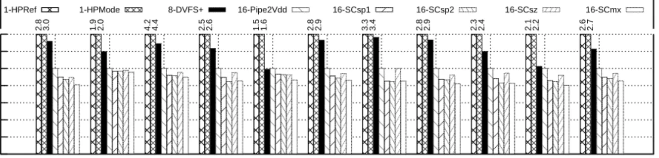
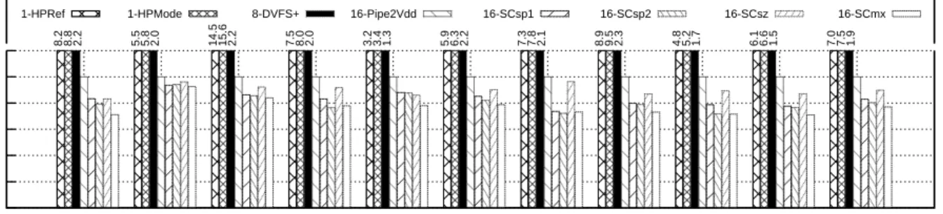
We use simulations of 16 cores to show that a design with ScalCores in EEMode is much more energy-efficient than one with conventional cores and aggressive DVFS: for approxi-mately the same power, ScalCores reduce the average execution time of programs by 31%, the energy (E) consumed by 48%, and the ED product by 60%. In addition, dynamically switching between EEMode and HPMode based on program phases is very effective: it re-duces the average execution time and ED product by a further 28% and 15%, respectively, over running in EEMode all the time.
The main contributions of this work are:
• The design of a voltage-scalable core based on our two observations • Pipeline changes to exploit the faster storage
• Evaluation of ScalCore and comparison to aggressive DVFS.
2.2 MOTIVATION
2.2.1 The Need for Voltage Scalability
In this work, we consider a high-performance, power constrained large manycore of the future, e.g. targeting cloud servers and high-performance computing. In such environments, users will continue to demand increasing energy efficiency while, at the same time, requiring different execution modes. Sometimes, a program will be highly parallel. In this case, we will attain highest performance by enlisting all the cores in the manycore — as long as they
run very energy-efficiently to avoid dark silicon. At other times, only a few cores will be able to run, as they execute mostly-serial sections. In this case, they will run with the highest performance, taking all the power budget of the chip.
Currently, there are two main approaches to address this conundrum: heterogeneity and DVFS. With heterogeneity, the chip contains some cores designed for energy efficiency and some for high performance. In the example above, the former would be used in the parallel section, while the latter in the mostly-serial one. The unused cores are power gated. An example of this approach is ARM’s big.LITTLE [28].
While this approach is useful, it is suboptimal. First, the partition between the two types of cores in the chip is fixed, and may not be the best one for a given application. Second, there is always a fraction of the chip area that is unused — in a big-little pair, either the area of the big core or that of the little one (which can be ≈30% of the big core’s area [29]). Finally, changing regimes involves migrating state, which has a performance overhead — e.g., ≈20µs [30].
DVFS [21, 22] uses cores of a single type and changes their Vdd and f values (and active core count) depending of the regime. However, this approach is also suboptimal. First, logic and storage structures scale differently with Vdd [27]. Hence, either at the high-Vdd or low-Vdd end, either the logic or the storage structures function suboptimally. Note that this is not fully solved by providing oneVdd domain for the core and one for the caches: the core pipeline still has both logic and storage structures. The second reason for suboptimality is that the lowestVdd with DVFS is still “high” compared to the most energy-efficient regime.
Such regime is at significantly-lowerVdds [31, 23, 32]. In this regime, Intel has prototyped the Claremont processor, which supports Vdd scaling all the way to 0.28V [25, 26]. Core and caches are in two differentVdddomains. However, a core designed to operate at such ultralow
Vdd needs to employ various circuit-level techniques that increase the area and, when the core operates at nominal Vdd, induce higher energy consumption.
This work goes deeper into the general DVFS approach. Our goal is to design a core that scales Vdd to values lower than conventional DVFS — but not as low as Claremont, to minimize design complexity, area cost, and power overhead at nominal Vdd. Such power overhead is unacceptable because it may trigger performance throttling, and makes the core non-competitive in HPMode. Note that our goal is not to compare the heterogeneity and DVFS approaches. Comparing our design to a heterogeneous one is outside our scope.
2.2.2 Logic and Storage Structures in the Pipeline
A pipeline contains multiple storage structures, such as the register file, load/store queue, or ROB. In general, these structures are built with static cells, which become failure-prone as the Vdd goes below a value called Vmin [23, 24]. There is a fundamental tradeoff between Vmin and cell size: if we want a lower Vmin, we need a cell with more transistors, with larger transistors, or FinFETs with more fins [33]. Hence, memory cells designed for lower Vmin consume higher power and energy when operating at nominal Vdd.
This problem worsens for the storage structures used in the pipeline because they are heavily multi-ported. In this case, more transistors are connected to the cross-coupled inverters that form the core of the storage cell. The resulting higher loading effect on the cross-coupled inverters makes the cell more sensitive to process variations [34, 8, 35]. Consequently, we need to increase the cell size, which increases its consumption at nominal
Vdd.
Since our goal is to keep the processor competitive at high Vdd operation, this is an unacceptable tradeoff. For example, Zhao et al. [35] show that going from a 1-fin 8T cell to a 2-fin 8T cell increases the leakage current by ≈20%. Moreover, our Spice simulations show that increasing the number of fins from 1 to 2 causes the 8T cell to consume 21% more power at nominal Vdd. This is shown in Figure 2.1, which plots the energy of 1-fin 8T and 2-fin 8T cells for different Vdds normalized to 1-fin 8T at the nominal Vdd of 0.9V. The figure corresponds to 22nm and an activity factor of 1. Overall, since we want the storage cells in the pipeline storage structures to be competitive at high Vdd, we propose to use finFET-based cells with a single fin.
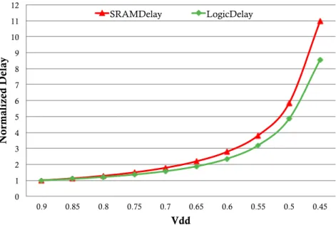
As we lower the Vdd, both logic and storage structures in the pipeline become slower. However, logic and storage structures scale differently [27]. This is shown in Figure 2.2, which we generate with Spice simulations of 22nm technology. The figure shows the increase in delay for a chain of FO4 inverters (LogicDelay) and for an 8T register-file bank (SRAMDelay) as Vdd decreases. The delay is the same and normalized to 1 at nominal Vdd. This plot includes the effect of random dopant fluctuation based on ITRS [14]. We see that storage structures become relatively slower. This is in line with the observation made by [36].
In related work, Dreslinski et al. [37] characterized the energy consumption of cores and caches at near-threshold voltage, and found that the energy-optimal Vdd for caches makes them 2-4x faster than the cores. We go beyond and exploit the different behavior of logic and storage structures within the pipeline.
0.00 0.20 0.40 0.60 0.80 1.00 1.20 1.40 0.9 0.85 0.8 0.75 0.7 0.65 0.6 0.55 N o rmal ize d Ene rg y Vdd 8T-1FIN 8T-2FIN
Figure 2.1: Effect of the number of fins in the FinFETs of the 8T cell on energy consumption for different Vdds.
2.3 SCALCORE CONCEPT 2.3.1 Main Ideas
Our goal is to design a core forVoltage Scalability, which means that it can flexibly work in a high-performance mode (HPMode) at nominal Vdd, and in a very energy-efficient mode
(EEMode) at low Vdd. The lowVdd is the lowest that can be sustained by the logic structures
in the pipeline (but not the storage ones) before their performance becomes substantially degraded — and without requiring changes to basic circuit structures, or changes to tran-sistor size or doping that can hurt the operation at nominalVdd. To attain our goal, we rely on three ideas: (i) provide separate lowVdds in the pipeline for logic and storage structures, (ii) further increase the lowVdd for the storage structures, and (iii) leverage the higher speed of the storage structures in the pipeline.
Two Low Vdds in Pipeline: Logic & Storage Designing storage cells to work at very low Vdd results in power inefficiency at nominal Vdd. Hence, we propose to modify the core to feed two Vdds to the pipeline in EEMode: (1) logic structures are powered at a very low
Vdd that still enables them to perform acceptably (Vlogic); and (2) storage structures such as the register file and load/store queue are connected to aVddthat is higher thanVlogic (and at least as high as their Vmin). With this design, the core operates with high energy-efficiency.
0 1 2 3 4 5 6 7 8 9 10 11 12 0.9 0.85 0.8 0.75 0.7 0.65 0.6 0.55 0.5 0.45 N o rmal ize d D el ay Vdd SRAMDelay LogicDelay
Figure 2.2: Increase in delay for logic and storage structures in the pipeline as we decrease
Vdd.
Moreover, when we do not want to operate in EEMode, we apply a higher, equal Vdd level to both logic and storage structures.
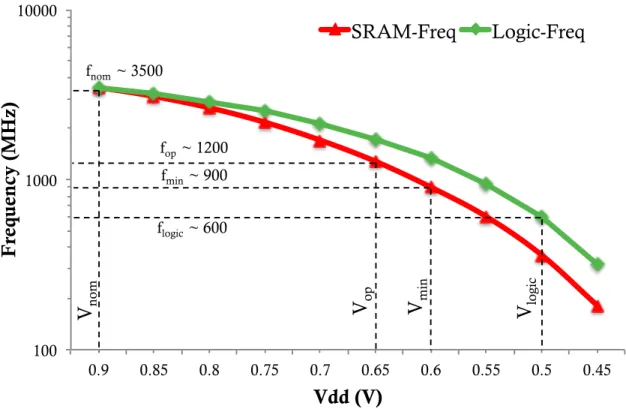
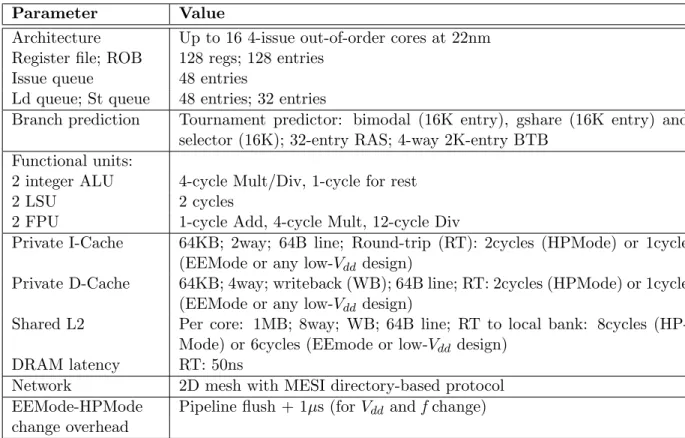
To determine theVdds, we proceed as follows. We take a four-issue out-of-order core (more details in Section 2.7) and use McPAT’s [38] high-performance process at 22nm to determine its fnomat the nominalVddof 0.9V. Such fnomis≈3.5GHz. Starting from this point, we use our Spice simulations of Figure 2.2 to generate the Vdd-f scalability curves for logic and storage structures. We then adjust these curves with the effects of systematic process variations, using VARIUS [39] with the systematic variation values of EnergySmart [40]. The resulting
Vdd-f curves are shown in Figure 2.3.
To pickVlogic, we observe that the logic delay curve in Figure 2.2 has a knee atVdd≈0.5V. Going below such value results in increasingly slower structures, which would cause the program to run substantially slower and consume substantially more leakage energy. This observation is consistent with the data in Kaul et al. [8]. Hence, in Figure 2.3, we set
Vlogic=0.5V, which corresponds to flogic ≈600MHz.
To find theVmin of the storage structures, we argue that upcoming storage cells are likely to be aggressively designed for energy efficiency, and hence for low Vmin. For example, Intel has attained SRAMs with Vmin=0.6V in 22nm [41] and 14nm [42]. Hence, we set
Vmin=0.60V, which in Figure 2.3 corresponds to fmin ≈900MHz. This operating point {Vdd=0.60V,f=900MHz}is thelowest pointthat we assume can be reached with conventional
100 1000 10000 0.9 0.85 0.8 0.75 0.7 0.65 0.6 0.55 0.5 0.45
Fr
equ
enc
y
(MH
z)
Vdd (V)
SRAM-Freq
Logic-Freq
V
opV
minV
log ic fop ~ 1200 fmin ~ 900 flogic ~ 600V
nom fnom ~ 3500Figure 2.3: Vdd-f curves for logic and storage structures.
DVFS with a singleVdd domain for the whole pipeline. While the Vdd looks aggressively low by today’s standards, we think it is plausible, given the need for energy efficiency in upcoming designs.
Further IncreaseVddfor the Storage Structures We can improve the energy efficiency of the EEMode if we consider the following traits of the EEMode regime:
• While the storage structures need a higher Vdd than the logic ones for safe operation (Vmin > Vlogic), the storage structures at Vmin can in fact operate faster than the logic structures atVlogic [27, 43]. This is seen in Figure 2.3.
• At this range ofVdds, a small increase inVddprovides a significant boost to the operating frequencyf.
• For storage structures at these low Vdds, the dominant component of power consump-tion is leakage.
These observations suggest that, in EEMode, a small further increase in the Vdd of the storage structures can make them significantly faster, while consuming only a little more
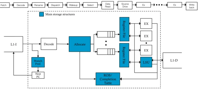
Next PC Decode Branch Pred. Allocate R eg ist er Fi le R eg ist er Fi le EX EX EX LSU ROB/ Completion Table
Main storage structures
Fetch Decode Rename Dispatch Wakeup Select Data
Read Source Drive Ex Ex Writeback
L1-I
L1-D
Figure 2.4: Pipeline of an out-of-order processor with the main storage structures.
power. A higherVddincreases the dynamic power comparatively more than the static power. However, since the dynamic power of storage structures in EEMode is small, the overall power will increase little.
Hence, we proposeScalCoreas a core where, in EEMode, theVdd of the storage structures is set to a voltage Vop that is higher than Vmin. Specifically, we set Vop > Vmin such that storage structures can operate at 2x the f of the logic structures (which use Vlogic). This is shown in Figure 2.3, where Vop≈0.65V and fop ≈1200MHz.
By setting the storage structures to Vop rather thanVmin, we will improve the IPC of the cores. The resulting lower execution time of the applications in turn reduces the leakage energy — not only of the cores, but also of the caches. This reduction more than compensates the small increase in dynamic energy in the storage structures induced by going from Vmin toVop.
Leverage the Higher Speed of Storage Finally, we exploit that storage structures are faster than logic ones in ScalCore’s EEMode in one of two ways:
• Without changing the core’s f, we fuse two consecutive pipeline stages that are dom-inated by storage structures into one. This reduces pipeline depth and improves the IPC.
• Without changing the core’s f, we enable more entries in critical storage structures in the pipeline, consuming some of the available time slack. This increases the exploitable
instruction-level parallelism (ILP) and memory-level parallelism (MLP), and improves the IPC.
In either case, in EEMode, all the stages of the ScalCore pipeline cycle at the same f. This keeps the pipeline relatively simple. Outside EEMode, we disable the fusing of pipeline stages and the larger storage structures, and use a single Vdd. The core becomes a plain out-of-order core optimized for high performance. It can use conventional DVFS (with a single Vdd in the pipeline) to vary its operating point.
Overall, ScalCore can flexibly deliver high performance in HPMode and high energy effi-ciency in EEMode. However, we need to carefully select which pipeline stages to fuse and which structures to resize , so that energy-efficiency is maximized. In addition, supporting this fusing and reconfiguration in EEMode should not hurt the performance in HPMode. The remainder of this section and the next addresses these two issues.
2.3.2 Analysis of Pipeline Stages
We analyze the pipeline stages that have storage structures to identify opportunities to improve EEMode operation. At low Vdd, Dreslinski et al. [37] showed that operating the L1 caches at a higherVdd than the core delivers energy efficiency. This same approach was used in Claremont [25, 26]. Hence, all of our low-Vdd designs (including the baseline) operate the L1 caches at Vop by default. With ScalCore, we go beyond and use two Vdd domains in the pipeline.
Figure 2.4 shows the pipeline of an out-of-order processor and identifies the main storage structures. They are the register file, allocation structures, load/store unit (LSU), ROB, and branch predictor. We now analyze each of these structures for possible enhancements when we operate them at Vop. The enhancements can consist of either fusing stages or increasing the size of structures. The implementation details are discussed later in Section 2.4.
Register File The critical path of a register file access in a pipelined design consists of two steps. In the first step, the operands are read from the data array into a buffer; in the second step, they are delivered to the execution units. This process takes at least two cycles in a typical high-frequency design [44]. By operating atVopin EEMode, we can enhance the register file in one of two ways: either reducing its access latency in cycles or increasing its size.
In the first case, we operate the two steps of a register file access at twice the speed, and fuse them into a single cycle. In the second case, we increase the size of the physical register file without changing the two cycles of access time.
Allocation Structures The allocation step primarily involves register renaming and in-struction dispatch. A detailed analysis of the critical path in renaming is performed by Palacharla et al. [45]. The authors found that the critical path in rename consists of reading the current mappings of the source registers in the Register Alias Table (RAT), followed by updating the mappings of the destination registers in the RAT. The dependence check among the registers currently being renamed is not in the critical path, and is implemented using low-power transistors, which reduces the dynamic power. Also, the design of the RAT is similar to the register file. Hence, we operate the rename unit at Vop in EEMode.
The rename delay in an out-of-order core is proportional to the core’s width. In a very wide core, the rename operation may take more than one cycle. However, for a core width of four like ours, renaming in a baseline design can be completed in a single cycle. Hence, in ScalCore, we can combine the rename and dispatch stages and fuse them into one cycle operating at Vop. Since the dynamic power consumption of the dispatch unit is low [46], the increase in Vdd to Vop has only a small effect. We do not change the size of the rename unit because we find that it does not have a critical resource whose size can be increased to improve performance.
Load/Store Unit (LSU) At a high level, the LSU consists of two stages, each taking one cycle. The first stage performs address generation, and the second one memory dis-ambiguation. Also, in parallel to the disambiguation, store instructions write values to the store buffer. The load/store queue in the LSU contains in-flight memory instructions and maintains the ordering between instructions.
Since the LSU takes two cycles and also has a resource (load/store queue) whose size can be increased, as we operate the LSU at Vop, we can do one of two things: either we fuse the two stages to reduce the latency to one cycle, or we increase the load/store queue size. When we fuse the two stages, stores write to the store buffer in half of a cycle. When we increase the load/store queue size, we also increase the store buffer size. Note that increasing the size of the load/store queue requires extra care, since it uses CAM structures to perform memory disambiguation (Section 2.4.1).
ROB We consider a merged register file-based renaming scheme as described in [44]. The ROB only acts as a completion table, keeping track of the in-flight instructions. The entries in the ROB are reserved on instruction dispatch and are freed on commit. The commit process in HPMode takes only one cycle. Hence, there is no obvious opportunity to reduce the latency in EEMode. However, we modify the size of the ROB in EEmode to enable more in-flight instructions. This allows us to exploit more ILP or MLP, based on the application.
The dynamic power of the ROB itself is low [46]. Hence the increase of the Vdd to Vop causes a modest increase in dynamic energy.
Branch Predictor Branch prediction in modern processors consists of a fast BTB to provide prediction in a single cycle, which is backed-up with a more complex and accurate branch predictor with a longer latency. In our baseline design, we have a tournament pre-dictor with a total size of 48K entries and a BTB of 2K entries. Although the BTB is structurally similar to a register file or cache, there is no obvious opportunity to further reduce its latency. While it is possible to take advantage of the faster operation at Vop by using a fancier branch prediction, it is out of our scope. Also, by simply increasing structure sizes, the expected improvement in IPC is small, considering the high baseline size [47, 48]. Hence, we do not optimize the branch predictor.
2.3.3 Summary
Based on the above analysis, Table 2.1 lists the pipeline structures that can be enhanced by ScalCore in EEMode, and the enhancement options. Note that a given structure cannot both run faster and be bigger at the same time. Outside EEMode, all structures are operated at the same Vdd, and at their baseline speed and size.
Table 2.1: Enhancements considered for different structures.
Structure Faster Bigger
Register File X X
Allocation Struc. X 7
Load Store Unit X X
ROB 7 X
Branch Pred. 7 7
2.4 SCALCORE DESIGN
To support the enhancements in Table 2.1, ScalCore requires some changes over conven-tional processors. We classify them into microarchitectural changes in the datapath and controlpath, and circuit changes. We consider each in turn.
Latch Stage 2a Latch Stage 2b Latch Enable Flow-through CLK Stage 3 Latch Stage 1 Latch
Latch 2a Latch Latch
CLK
Stage 3
Latch
Stage 1
Latch 2b
Vnom Vnom Vnom Vnom
Vlogic Vop Vop Vlogic 0 Enable Flow-through 1 HPMode EEMode
Figure 2.5: Datapath changes in ScalCore: Fusing pipeline stages using a flow-through latch. The shaded components are disabled.
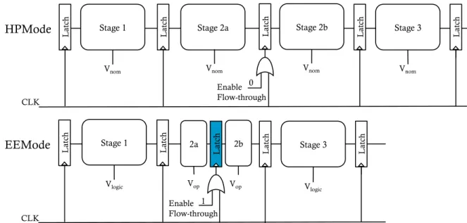
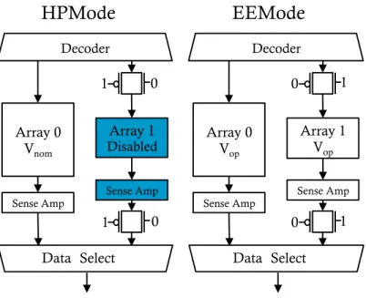
Reduction in Latency Fusing two consecutive pipeline stages in EEMode is accomplished by transforming the latch that sits in between them into a transparent (or flow-through) latch [49, 50]. This is done by ORing the clock to the latch with an Enable Flow-through signal. When the signal is set to logic one, the latch is transparent.
The logic design is shown in Figure 2.5. In HPMode (upper chart), Stages 2a and 2b take one cycle each, and operate at nominal voltage (Vnom) like the other stages. The Enable Flow-through bit in the OR gate is set to logic zero. This causes the latch to be controlled by the clock.
In EEMode (lower chart), Stages 2a and 2b are fused together to execute in a single cycle. The Enable Flow-through bit is set to logic one, which makes the latch transparent. In addition, Stages 2a and 2b operate at Vop, which is higher than the Vlogic used in Stages 1 and 3.
This OR gate is added to the latches connecting the pairs of stages to be fused: (i) the two stages of a register file access, (ii) rename and dispatch, and (iii) the two stages in the LSU. Designs based on flip-flops can be modified in a similar manner, by providing a bypass path that is enabled in EEMode.
Bigger Structures The size of a storage structure in ScalCore is increased by enabling an additional array with transmission gates. This general approach was proposed by Buyukto-sunoglu et al. [51] for issue queues. By toggling the input to the transmission gates, we can
Array 0 Vnom
Decoder
Array 1 Disabled
Sense Amp Sense Amp
Data Select
HPMode
0 1 0 1 Array 0 Vop Decoder Array 1 VopSense Amp Sense Amp
Data Select
EEMode
1 0 1 0Figure 2.6: Datapath changes in ScalCore: Increasing the size with transmission gates. The shaded components are disabled.
easily enable or disable the new array. Figure 2.6 shows an example of a structure with an original array (Array 0), and an additional one (Array 1) connected with transmission gates. In HPMode (left chart), the transmission gates disable Array 1, while Array 0 operates at
Vnom. In EEMode (right chart), the transmission gates enable Array 1. Both arrays are active and run at Vop.
With this design, the register file, load/store queue, store buffer, and ROB can use more entries in EEMode than in HPMode. CACTI analysis [52] shows that, at the higherVop, we could increase the structure sizes substantially and still meet the cycle time. However, very large structures incur area and leakage overheads, and are hard to use cost-effectively. As we will see, a possible design is to increase the size of these structures by 50% in EEMode.
We make special arrangements for the load/store queue, since it uses CAM structures to perform memory disambiguation. Specifically, to reduce complexity, ScalCore uses a segmented load/store queue [53] with two segments. In HPMode, only one segment is active and the other is power gated. Hence, the delay and power in HPMode are not impacted. In EEMode, both segments are active and are sequentially searched on a request. Since the segments operate at Vop, both segments are searched in a single cycle.
In EEMode, the dynamic power of the load/store queue increases only for the searches that overflow into the second segment. Also, techniques like low-swing, selective precharge of search line/matchline reduce the dynamic power of CAM by more than 50%, with no
delay impact over a conventional design [54]. By using such techniques, the dynamic power component becomes small even in the baseline. Hence, the increase in load/store queue size causes only a small increase in the dynamic energy.
2.4.2 Controlpath Microarchitectural Changes
Reduction in Latency Reducing the latency of some operations has an impact on the scheduling of various tasks in the pipeline. So, we need to modify the control logic responsible for those tasks. Specifically, in EEMode, by reducing the register file read latency (which includes the source drive of operands) from two to one cycle, the execution units receive operands in one cycle, and hence can begin execution one cycle earlier. In addition, as the execution finishes a cycle earlier, the dependent instructions can be woken up and scheduled earlier. Hence, the execution schedule time and the generation of the wakeup signal need to be updated based on the mode of operation. Similarly, to enable the speculative issue of load-dependent instructions, the issue logic should be updated with the new latency of the LSU.
Reducing the latency of the allocation operation does not have an obvious direct impact on the scheduling of tasks. The process of renaming and dispatching instructions in order can proceed in the same manner in both modes.
Therefore, the only controlpath modifications required are to ensure that the part of the issue-queue state machine responsible for generating ready signals accurately reflects the mode of operation. The issue queue already contains functionality to generate the wakeup signal at different times based on the latency of the functional unit (e.g., ADD vs. DIV) [44]. Hence, by modifying the counters used for this process, we ensure correct scheduling in both HPMode and EEMode.
Bigger Structures The availability of a bigger resource should be conveyed to its corre-sponding resource manager to enable its usage. In EEMode, the sizes of the register file, load/store queue, store buffer, and ROB are higher. To benefit from the bigger physical register file, the list of free registers in the rename unit must be updated. The list of free registers is typically maintained as a circular buffer with head and tail pointers, which can be resized based on the mode of operation.
The dispatch unit is responsible for checking various execution resources and stall in case of unavailability. It maintains counters for the availability of each resource. To indicate the sizes of the current ROB, load/store queue, and store buffer, we just need to update these counters based on the mode of operation. Overall, therefore, the changes required in
the controlpath for bigger structures involve reconfiguring the counters in the rename and dispatch stages.
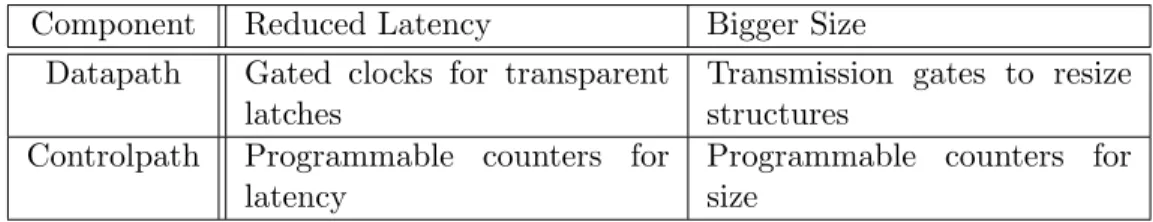
Table 2.2 summarizes the microarchitectural changes in the datapath and controlpath to enable our enhancements.
Table 2.2: Microarchitectural changes in ScalCore.
Component Reduced Latency Bigger Size
Datapath Gated clocks for transparent
latches
Transmission gates to resize structures
Controlpath Programmable counters for
latency
Programmable counters for size
2.4.3 Circuit Changes
The circuit changes involve supporting dual voltage rails and level converters.
Dual Voltage Rails In ScalCore, each pipeline stage is connected to one of twoVdd rails, as shown in Figure 2.7. All the storage-intensive stages are connected to one rail. They are the two stages of register file access, the rename stage, the dispatch stage, the two stages of LSU access, and the commit stage. The other stages are connected to the other rail. Each rail is set to the required Vdd level, based on the mode of operation. In EEMode, the storage-intensive stages receive Vop, while the rest receive Vlogic; outside EEMode, both rails supply the same voltage.
Storage
Stage 2a Stage 2b Storage Logic
Stage 1
HPMode: V1 = V2 = Vnom EEMode: V1 = Vlogic; V2 = Vop
V1 V2 Latch w/ Level C on v. Latch Latch Logic Stage 3
Figure 2.7: ScalCore pipeline with dual voltage rails.
These storage-intensive stages share theVdddomain with the L1 caches which, as indicated in Section 2.3.2, also operate at Vop in EEMode. As a result, there is no need to add any
additional voltage regulator in ScalCore over the baseline design. Note that the L1 caches are laid out together with the pipeline in current designs.
Level Converters All the stages in ScalCore always operate at a commonf. This simplifies the design by avoiding multiple clock trees and synchronization overhead across stages. However, consecutive pipeline stages may operate at differentVdd levels in EEMode. Hence, a level converter is required on the boundary between a stage at Vlogic and one at Vop, to provide full swing input to the higher Vop domain. Note that the difference in Vdd levels is only 150mV.
Level converters can be designed as part of the latches or flip-flops that separate the stages (Figure 2.7). The design of a level converter is shown in Figure 2.8. It is based on [55], where pulsed half-latch level converting flip-flops are shown to be efficient, both in area and in energy-delay, compared to asynchronous level conversion in a dual-Vdd system.
Vlogic Vop d q (inv) ck ck clk
Figure 2.8: Level converter for up-conversion.
2.5 IMPLEMENTATION CONSIDERATIONS
This section considers three implementation issues: the transition between modes, a sum-mary of ScalCore overheads, and a comparison to Intel Claremont.
2.5.1 Transition Between Modes
In highly-parallel sections, all the cores in a large manycore are powered-on and run in EEMode. In sections with little parallelism, only a few cores are powered-on and run in HPMode, using all the power budget of the chip. While in HPMode, ScalCore can also use DVFS.
ScalCore provides a simple way to reconfigure the pipeline between the two modes. First, pipeline reconfiguration can only occur when the pipeline is empty. Consequently, recon-figuration requires a pipeline flush. Such a flush can take a variable number of cycles — e.g., depending on whether there are pending writes in the store buffer (pending reads are squashed). However, the average flush is not likely to take more than several tens of cycles. Second, we need to change the f and Vdd of the core. Specifically, from a common Vdd in all stages in HPMode, we transition to Vop for the storage-intensive stages and Vlogic for the others in EEMode (or vice-versa). This transition uses conventional DVFS mechanisms. Its overhead is likely to be modest in the future, as increasing DVFS speed is an active area of research and development. In our evaluation, we set this overhead of changing f and Vdd between modes to 1 µs. Note that pipeline stages do not switch Vdd rails; ScalCore merely changes the rails’ voltage.
Overall, the overhead of transitioning from EEMode to HPMode and vice-versa is small. The reconfiguration can be triggered either in hardware by the power management unit, or in software by the operating system or program.
2.5.2 Summary of ScalCore Overheads
Table 2.3 summarizes the ScalCore overheads and their impact on HPMode. The first issue is dualVdd rails. Their main overheads are the additional area they take and the need to customize their layout/routing, since automatic tools may not be able to handle them. One implementation of dual rails [56] estimates the area cost to be ≈5% of the core.
Table 2.3: Summary of ScalCore overheads.
Issue Type of Overhead Impact on HPMode
Dual Vdd rails 1) Custom layout and routing. 2) Area increase ≈5% area [56]
Level converters 1) Carefully manage clock skew/timing. 2) Add
gates in critical path
≈5% delay [55]
Fusing Pipeline
Stages
1) OR gate added to the clock signal for each latch connecting fused stages. 2) Control logic for counters for latency
Tiny area and power
Increasing Array Sizes
1) Additional array. 2) Transmission gates to enable/disable additional array. 3) Segmented ld/st queue. 4) Control logic for counters for size
Area of power-gated ar-ray. Tiny power and de-lay [51]
The second issue is level converters. They require carefully managing the clock skew and timing across domains. Moreover, they add a few gates to the pipeline stage. Based on
Ishihara et al.’s [55] work, we estimate a delay impact in HPMode of ≈5%. The additional area and power of the level converters is negligible [55].
The third issue is fusing pipeline stages. It requires an OR gate added to the clock signal for each latch connecting fused stages, and control logic for counters for latency (Section 2.4.2). In HPMode, it adds a tiny area and power overhead but no delay in the critical path.
A fourth issue is increasing array sizes. It requires an additional array, transmission gates to enable/disable the additional array, a segmented load/store queue, and control logic for counters for size (Section 2.4.2). In HPMode, the additional array is power gated, but takes up area. The additional logic introduces only tiny power and delay overheads. Buyuktosunoglu et al. [51] show that the transmission gate delays are negligible. Their design is more involved than ours in that they get multiple, dynamically variable latencies, which require careful synchronization with the rest of the pipeline. In our case, we only have two configurations, and the large one has ample timing slack. Similarly, Park et al.’s [53] segmented load/store queue is more involved because disambiguation can take a variable number of cycles, while ours always takes one cycle.
Finally, ScalCore introduces design complexity and verification costs, which are hard to quantify.
2.5.3 Comparison to Intel Claremont
Table 2.4 compares Intel’s Claremont prototype [25, 26] to ScalCore. A main difference is that Claremont targets a very wide Vdd operating range (1.2V to 280mV) while ScalCore targets a more modest range (0.9V to 0.5V). As a result, Claremont uses more aggressive techniques, including manually prioritizing the placement of logic paths that have a high
Table 2.4: Comparing Intel Claremont to ScalCore.
Trait Claremont ScalCore
Vdd range Very wide: 1.2V to 280mV Wide: 0.9V to 0.5V
Focus Circuit techniques: Architectural techniques:
1) Variation aware pruning &
beefing-up of cells.
1) Separate Vdd for memory
inten-sive pipe stages. 2) Circuits optimized for reliability
at ultralowVdd
2) Fuse pipeline stages. 3) Increase array sizes
Vdd domains 1 for the pipeline + 1 for the L1 1 for the memory intensive pipe
stages and L1 + 1 for the other pipe stages
percentage of interconnect, or using two level-converters in series to bring the voltage to high Vdd.
Another difference is that Claremont’s focus in on circuit techniques, while ScalCore’s is on architectural techniques. Claremont includes variation-aware selective pruning and beefing-up of the standard cell library, and circuits optimized for reliability at ultralow Vdd — e.g., avoiding wide transmission-gate multiplexers and circuits with high transistor stacks. The result of needing to reach an ultralow Vdd is device area bloat.
ScalCore focuses on architectural techniques such as a separateVdd for memory-intensive pipeline stages, fusing pipeline stages, and increasing array sizes.
Although the number of Vdd domains in both designs is the same, they are organized differently. Claremont has one domain for the pipeline and one for the L1; ScalCore has one for the memory-intensive pipeline stages plus the L1, and one for the rest of the pipeline stages.
2.6 IMPLICATIONS ON APPLICATIONS
The performance of a core is dependent on various factors, including the frequency, cache/memory latency, pipeline depth, and pipeline structures. In ScaleCore, we modify the pipeline depth and sizes of structures in EEMode. We now qualitatively discuss the impact of these modifications on application performance. We will discuss the detailed evaluation results later in Section 2.8.
2.6.1 Pipeline Stage Fusion
In EEMode, ScalCore can perform register access, rename-dispatch, and LSU handling in one cycle each, rather than in two cycles each. In total, the pipeline depth reduces by three cycles for load/store instructions and by two cycles for others. This reduction has a few implications, as noted by Tullsen et al. [57]. First, it reduces the branch misprediction penalty by 2 cycles. Second, it results in fewer instructions from the mispredicted path in the pipeline, which saves energy and resources. Third, registers are now held for a shorter duration, reducing the contention for physical registers during renaming. Finally, reducing the LSU latency also helps the optimistic issue of load-dependent instructions that assume a cache hit.
Overall, these effects result in an increase in the average IPC for a broad range of appli-cation types — especially for integer appliappli-cations, which have more branches.