A Graphical User Interface Implementation of
Second Order Sigma- Delta Analog to Digital
Converter with Improved Performance
Parameters
Prateek Verma#1, Anil Kumar Sahu*2,Dr. Vivek Kumar Chandra*3,Dr. G.R.Sinha*4
#1
M.E. Research Scholar, VLSI Design, Electronics & Telecommunication Department, Shri Shancharacharya Technical Campus, Bhilai, Chhattisgarh, India
#2
Assistant Professor, Electronics & Telecommunication Department, Shri Shancharacharya Technical Campus, Bhilai, Chhattisgarh, India
#3
Associate Professor and Head, Electrical & Electronics Department, Chatrapati Shivaji Institute of Technology, Durg Chhattisgarh, India
#4
Professor and Associate Director, Faculty of Engineering & Technology, Shri Shancharacharya Technical Campus, Bhilai, Chhattisgarh, India
Abstract—Analog to Digital Converters are widely used in the field of VLSI and are mainly used in the applications like audio, instrumentation, seismic, voice etc which requires higher valueof resolution. For such applications, ADC’s can be used based on
Nyquist Rate modulators (where sampling is done with twice the sampling frequency) or Sigma-Delta modulators (where sampling is
done with 15-20 times the sampling frequency). ADC based on sigma-delta modulators is attractive for VLSI implementation because
they are not so sensitive of circuit non-idealities and component mismatch. However, issues such as clock jitter and excess loop delay
become great challenges to the designer, especially at high sampling frequency. Special design should be applied to overcome these
problems. Sigma-Delta modulator can be of different orders like 1st order, 2nd order etc and can be continuous time (less power
consumption) or Discrete Time (less sensitive to non- idealities). This work demonstrates a Graphical User Interface (GUI) of 2nd
order Sigma-Delta modulator which is used to check the non-idealities of the circuit. Here the model is based on the behavioral
modeling of the parameters with the help of Matlab - Simulink and the parameters like Signal to Noise Ratio (SNR) & Effective
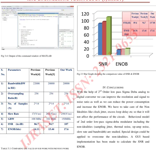
Number of Bits (ENOB) (which in turn gives the Resolution) are calculated. The value of SNR and ENOB are found to be 107.88 dB
and 17.61 bits respectively in comparison to the 89.4, 94.7 dB & 14.56, 15.44 bits respectively of the previous work. Since the value of
SNR and ENOB are increased it makes the respective signal power and Resolution better. The Graphical User Interface (GUI) of
Page 105 Keywords—Sigma-Delta ADC, GUI, SNR, ENOB
I. INTRODUCTION
Analog-to-digital converters are important components in
applications requiring the interface between analog and digital
domains. There are numerous applications such as digital
radio systems, military and medical sensors, and wire- line
and wireless communication systems. There are a number of
different ADC architectures available to accomplish the data
conversion task; however, no single architecture is suitable for
all applications. These architectures span a range of intended
resolutions and conversion speeds. Meanwhile, wireless and
wire- line applications need the bandwidth of the signal to be
[image:3.612.43.284.370.602.2]in megahertz and better resolution with 12 or more bits. [1]
Fig 1.1: Applications of different types of ADC [2]
1.1 Low-pass sigma delta ADC
ADC based on 2nd order sigma-delta modulators is
attractive for VLSI implementation because they are resistant
to the circuit non- idealities and component mismatch.
However, issues such as clock jitter and excess loop delay
become great challenges to the designer, especially at high
sampling frequency. Special design should be applied to
overcome these problems. Sigma-delta modulation has
demonstrated to be very suited interfaces for the
implementation of various Analog to Digital in many different
electronic systems, covering a large number of applications
from instrumentation to telecom.
II. PROPOSED METHODOLOGY
2.1 Proposed Methodology during the Tenure of
Research Work
Delta-sigma (ΔΣ; or sigma-delta, ΣΔ) modulation is a method
for encoding analog signals into digital signals or
higher-resolution digital signals into lower-higher-resolution digital signals.
A 2nd Order Sigma-Delta A/D Converter consists of the
following
A loop filter or loop transfer function H(s) A clocked quantizer
A feedback digital to analog converter (DAC).
A loop filter H(s) provides a noise-shaping function for the
analog input signal before it is sampled and quantized by an
ADC. The digital output signal is then converted back to
analog signal by a DAC and feedback to the input for
subtraction to form a closed-loop operation. The input signal
is sampled after being filtered through the loop filter,
significant suppression at aliasing frequencies can be
obtained.Proposed work will use 2nd order CT sigma delta
modulator ADC and system modeling of no idealities and
integrators inside the topology to realize the 2ndorder system.
[image:4.612.52.559.86.668.2]Also the output noise value is less in less frequency.[2]
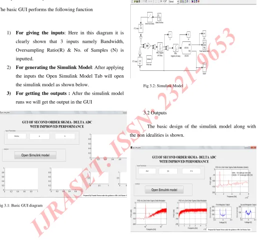
[image:4.612.68.257.183.335.2]Fig 2.1: Output noise of first order vs. second order sigma delta ADC
Fig.2.2: Second-Order Sigma-Delta ADC [6]
NO
YES
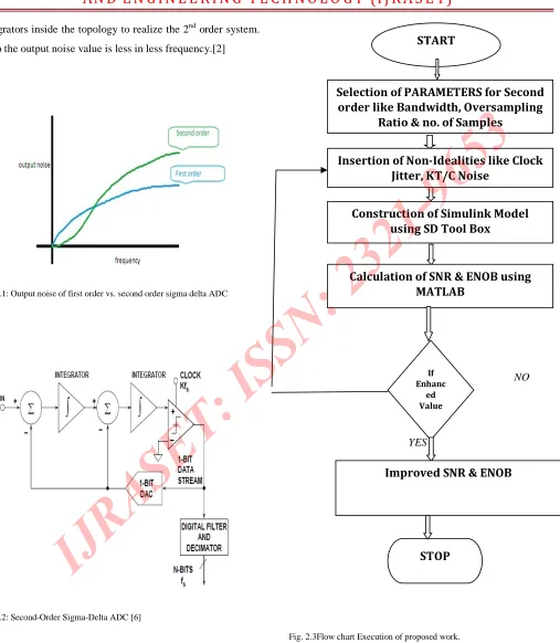
Fig. 2.3Flow chart Execution of proposed work.
START
Selection of PARAMETERS for Second order like Bandwidth, Oversampling
Ratio & no. of Samples
Construction of Simulink Model using SD Tool Box
Calculation of SNR & ENOB using MATLAB
If Enhanc
ed Value
STOP
Insertion of Non-Idealities like Clock Jitter, KT/C Noise
Page 107 III. RESULTS
3.1 Experimental Setup
The basic GUI performs the following function
1) For giving the inputs: Here in this diagram it is
clearly shown that 3 inputs namely Bandwidth,
Oversampling Ratio(R) & No. of Samples (N) is
inputted.
2) For generating the Simulink Model: After applying
the inputs the Open Simulink Model Tab will open
the simulink model as shown below.
3) For getting the outputs : After the simulink model
runs we will get the output in the GUI
Fig 3.1: Basic GUI diagram
Fig 3.2: Simulink Model
3.2 Outputs
The basic design of the simulink model along with
[image:5.612.39.556.132.613.2]the non idealities is shown.
Fig 3.4: Output of the command window of MATLAB
TABLE 3.1: COMPARING THE VALUE OF OUR WORK WITH PREV
S.
No.
Parameters Previous
Work[4]
Previous
Work[5]
1) Bandwidth(BW
in HZ)
22000 20000
2) Oversampling
Ratio(R)
256 256
3) No. of Samples
(N)
2^14 2^14
4) Slew Rate 17(V/us) 202(V/us)
5) GBW 100 MHz 102 MHz
6) SNR (in dB) 86.7 94.7
7) ENOB(bits) 14.11 15.44
[image:6.612.31.575.87.609.2]F OUR WORK WITH PREVIOUS WORK
Fig.3.5 Bar Graph showing the comparison value of SNR & ENOB
IV. CONCLUSIONS
With the help of 2nd Order low pass Sigma Delta analog to
digital converter we can improve the resolution and signal to
noise ratio as well as we can reduce the power consumption
and increase the ENOB. We have to take care of the Non
Idealities like clock jitter, excess loop delay etc so that it will
not affect the performance of the circuit. Behavioral model
of 2nd order low-pass sigma-delta modulator including the
non-idealities (sampling jitter, thermal noise, op
slew rate and bandwidth) are studied. Special design could be
applied to overcome the non-idealities. A GUI based
implementation has been made to calculate the SNR and
ENOB.
Here the model is based on the behavioral modeling of
the parameters with the help of Matlab
parameters like Signal to Noise Ratio (SNR) & Effective
Number of Bits (ENOB) (which in turn gives the Resolution)
0
20
40
60
80
100
120
SNR
ENOB
Our Work 20000 256 2^14202(V/us) 250(V/us)
102 MHz 150MHz
107
17.6
Bar Graph showing the comparison value of SNR & ENOB
ONCLUSIONS
Order low pass Sigma Delta analog to
digital converter we can improve the resolution and signal to
noise ratio as well as we can reduce the power consumption
ase the ENOB. We have to take care of the Non
like clock jitter, excess loop delay etc so that it will
not affect the performance of the circuit. Behavioral model
delta modulator including the
ng jitter, thermal noise, op-amp noise,
slew rate and bandwidth) are studied. Special design could be
idealities. A GUI based
implementation has been made to calculate the SNR and
Here the model is based on the behavioral modeling of
the parameters with the help of Matlab- Simulink and the
parameters like Signal to Noise Ratio (SNR) & Effective
[image:6.612.28.298.322.599.2]Page 109 are calculated. The value of SNR and ENOB are found to be
107.88 dB and 17.61 bits respectively in comparison to the
94.7 dB & 15.44 bits respectively of the previous work. Since
the value of SNR and ENOB are increased it makes the
respective signal power and Resolution better.
REFERENCES
[1] Verma, Prateek, and Anil kumar Sahu. "A Graphical User Interface(GUI) implemented Low-pass continous time Sigma-delta ADC with improved SNR & ENOB." International Journal of Advanced Research in Computer Science and Software Engineering 4.6 (2014): 144-149.
[2] S. Yan, E. Sanchez-Sinencio “A continuous-time sigma-delta modulator with 88-dB dynamic range and 1.1-MHz
signal bandwidth” IEEE Journal of Solid-State Circuits.Feb 2004.
[3] http://www.eeweb.com/blog/carmen_parisi/balancing-the-tradeoffs-in new-generation- adcs
[4] Brigati, S., Francesconi, F., Malcovati, P., Tonietto, D., Baschirotto,A., & Maloberti, F. (1999, July). Modeling sigma-delta modulator non-idealities in SIMULINK (R). In Circuits and Systems, 1999. ISCAS'99.
[5] Ren, Mingyuan, et al. "The Design of High Performance, High Resolution Two-Order Delta-Sigma Modulator." Sensors &Transducers,Vol.22,Special Issue, June 2013, pp.155-162.
[6] ADC Architectures III: Sigma-Delta ADC Basics by Walt Kester.( MT-022 TUTORIAL)
[7] Bandopadyay, T. K., Manish Saxena, and Raghav Shrivastava. "Sigma Delta Modulator with Improved Performance through Evolutionary Algorithm." International Journal of Science and Research (IJSR) Volume 2 Issue 3, March 2013.
[8] Benabes, Philippe. "Accurate time-domain simulation of continuous-time sigma–delta modulators." Circuits and Systems I: Regular Papers, IEEE Transactions on 56.10 (2009): 2248-2258.
[9] Bolatkale, Muhammed, et al. "A 4 GHz continuous-time ADC with 70 dB DR and 74 dBFS THD in 125 MHz
BW." Solid-State Circuits, IEEE Journal of 46.12 (2011): 2857-2868.
[10] Chaudhari, Jaydip H. "Design and Simulation of 1-bit Sigma Delta ADC in 0.18 um CMOS Technology." IJCAIT 2.1 (2013): 50-53.
[11] C. H. E. N. Zhicai, Mathew Bond, and Nijad Anabtawi. "Design of a Second Order Continuous Time Sigma Delta Modulator with Improved Dynamic Range." Final Project of Oversampling Class, Fall 2007 Arizona State University.
[12] Garcia, Julian, Saul Rodriguez, and Ana Rusu. "A Low-Power CT Incremental 3rd Order/spl Sigma//spl Delta/ADC for Biosensor Applications." Circuits and Systems I: Regular Papers, IEEE Transactions on 60.1 (2013): 25-36.
[13] Gerfers, Friedel, Maurits Ortmanns, and Yiannos Manoli. "A 1.5-V 12-bit power-efficient continuous-time third-order ΣΔ modulator." Solid-State Circuits, IEEE Journal of 38.8 (2003): 1343-1352.
[14] Hart, Adam, and Sorin P. Voinigescu. "A 1 GHz Bandwidth Low-Pass ADC With 20–50 GHz Adjustable Sampling Rate." Solid-State Circuits, IEEE Journal of 44.5 (2009): 1401-1414.
[15] Kumar, Y. B. N., et al. "A 1.96-mW, 2.6-MHz bandwidth discrete time quadrature band-pass ΣΔ modulator." Circuits and Systems (ISCAS), 2013 IEEE International Symposium on. IEEE, 2013.
[16] Lim, Huey Jen, Simon Sheung Yan Ng, and Minkyu Je. "Bandpass Continuous-Time Delta-Sigma Modulator for Wireless Receiver IC." International Journal of Information and Electronics Engineering, Vol. 3, No. 1, January 2013.
[17] Shaoyu MA, Yan Han, You Cai A 3.3V 18 Bit Digital Audio Sigma- Delta ADC in 0.18 um CMOS Process 2007.
[19] Nilchi et al(2013,May), A low power delta sigma modulator using a charge-pump integrator IEEE transaction on circuits and systems.
[20] Prateek Verma & Anil Kumar Sahu, A 22 kHz Bandwidth and 107dB SNR Low-pass Sigma-delta
ADC. International Conference “SHAASTRATH” on
23rd -24th March 2014 at Rungta Group of Institutions, Raipur
[21] Prateek Verma, Arun Kumar Sonwani & Anil Kumar Sahu, A 16 Bit ENOB and 98 dB SNR 2nd order Low-pass Sigma-delta ADC,International Conference on Emerging Trends in Electrical, Electronics, Instrumentation & Computer Engineering (ETEICE), BIT Raipur 27th March 2014
[22] SIMULINK and MATLAB Users Guides, The MathWorks, Inc.
[23] Zhu, Yingbo, et al. "Fourth-order discrete-time variable centre frequency bandpass sigma-delta modulator." IEEE Asia Pacific Conference on Circuits and Systems (2006: Singapore) APCCAS 2006. 2006.
[24]
[25]
[26] Proceedings of the 1999 IEEE International Symposium on (Vol. 2, pp. 384-387). IEEE.
new-yuan, et al. "The Design of High Performance, High Resolution Two-Order Delta-Sigma Modulator." Sensors &Transducers, Vol.22, Special Issue, June 2013, pp.155-162.
![Fig 1.1: Applications of different types of ADC [2]](https://thumb-us.123doks.com/thumbv2/123dok_us/8587640.862899/3.612.43.284.370.602/fig-applications-different-types-adc.webp)