Electron wave-function spillover in self-assembled InAs/ InP quantum wires
J. Maes*and M. Hayne
Pulsed Field Group, Laboratory of Solid State Physics and Magnetism, K.U. Leuven, Celestijnenlaan 200D, B-3001 Leuven, Belgium
Y. Sidor, B. Partoens, and F. M. Peeters
Departement Natuurkunde, Universiteit Antwerpen (Campus Drie Eiken), Universiteitsplein 1, B-2610 Antwerpen, Belgium
Y. González, L. González, D. Fuster, and J. M. García
Instituto de Microelectrónica de Madrid (CNM-CSIC), C/Isaac Newton 8, 28760 Tres Cantos, Madrid, Spain
V. V. Moshchalkov
Pulsed Field Group, Laboratory of Solid State Physics and Magnetism, K.U. Leuven, Celestijnenlaan 200D, B-3001 Leuven, Belgium
(Received 4 December 2003; revised manuscript received 19 February 2004; published 15 October 2004)
Charge confinement in InAs/ InP self-assembled quantum wires is studied experimentally using photolumi-nescence in pulsed magnetic fields and theoretically using adiabatic theory within the effective-mass approxi-mation, taking into account the strain in the samples. We show both experimentally and theoretically that, in spite of the large conduction band offset, the electron wave function is significantly spilled out of the wire in the wire height direction for thin wires. Furthermore, for a wire thickness of up to 8 monolayers, the electron spillover is inversely related to the wire height. These effects are due to the large zero point energy of the electron. As the wire becomes thicker, the decrease in confinement energy is reflected in a reduction of the electron wave-function extent.
DOI: 10.1103/PhysRevB.70.155311 PACS number(s): 73.21.La, 78.55.Cr, 78.67.Hc
I. INTRODUCTION
Under certain growth conditions, uniform arrays of self-assembled quantum wires can be obtained by solid source molecular beam epitaxial (MBE) deposition of InAs on an InP substrate.1–4 InAs quantum wires embedded in an InP matrix are a type-I system, and act to confine the electron and hole to the InAs wires5 They are promising candidates
for optical applications at the telecommunication wave-lengths (1.3 and 1.55m), although they generally show a broad photoluminescence (PL) spectrum consisting of sev-eral peaks that are attributed to quantum wires of heights which differ by a discrete number of monolayers.2Here,
in-formation on the confinement of excitons in such wires is obtained by careful analysis of the energy shift of the PL peaks in high magnetic fields共艋50 T兲 and by a strain de-pendent effective-mass approximation.6–8 Although both
conduction and valence band offsets are large (0.657 and 0.35 eV, respectively) and thus electrons and holes are ex-pected to be strongly confined to the InAs wire, we find that for very flat wires a large fraction of the electron wave func-tion is located in the InP barrier material. In this regime, the exciton wave-function extent is inversely related to the wire height. Such a wave-function penetration into the barrier ma-terial has already been predicted and observed for In0.1Ga0.9As/ GaAs quantum wells,9 T- and V-shaped GaAs
quantum wires,10–13Ge/ Si quantum dots,14 and other
nano-structures, where the charge confinement is relatively weak in the absence of a magnetic field:15,16much weaker than in
the InAs/ InP quantum wires under study. In these systems, the wave-function spillover was investigated mainly
theoretically10,12,16or by PL in zero field14or low magnetic
fields up to 12 T.9,11A detailed overview of exciton confine-ment in GaAs quantum wires is given by Akiyama.13In
ad-dition, the dependence of the wave-function penetration on the dimensionality of the system was studied and shows that, due to the lower dimensionality of the quantum wire, the confinement energy is increased and thus the wave-function penetration into the barrier is larger as compared to a quan-tum well with similar band offsets.10,15,17Three methods of
fabricating quantum wires, other than the self-assembly pro-cess mentioned here, have been applied to the In共Ga兲As/ InP system. The first is the deposition of an unstrained In0.53Ga0.47As/ InP multi-quantum-well on a vicinal (001)
InP substrate, which leads to very thin quasi-one-dimensional filaments18in which exciton wave function
pen-etration is expected due to the monolayer thickness,8 but to
date, has not been quantitatively studied. A second method is based on the deposition of a lithographically patterned stres-sor on top of an InGaAs/ InP quantum well,19 and the third
method relied on the prepatterning of the substrate.20In this
way, large quantum wires have been created for which, con-sequently, no wave-function penetration is expected. In the self-assembled InAs/ InP system (both wires and dots), a wave-function spillover into the barrier material was not ex-pected and thus had not been considered to date,2,21,22 but it
II. GROWTH OF QUANTUM WIRES
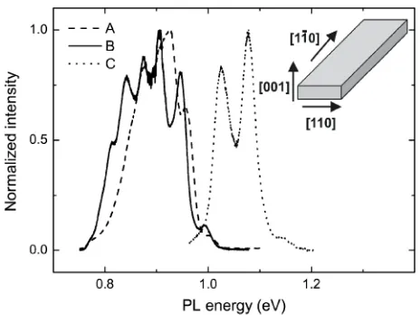
We report on the investigation of three different quantum wire samples. The first sample(A)was fabricated by atomic layer molecular beam epitaxy. A 200 nm thick InP buffer layer was grown on top of an InP substrate at 430 ° C. The temperature was kept constant during the deposition of 2.5 monolayers(ML)of InAs. The sample was subsequently annealed for 2 min at 530 ° C. For this sample, it was during the annealing that the quantum wires formed. Afterwards, the temperature was lowered again to the original value for deposition of the 50 nm thick InP capping layer. For the second sample (B), the growth was similar but at different temperatures. The deposition temperature was 430 ° C and the annealing temperature was 560 ° C. In sample C, InAs was grown at 515 ° C. In this sample, due to the elevated temperature, quantum wires were formed during growth after 1.7 ML of InAs was deposited, without any further annealing step. Immediately after wire formation, the InAs growth was interrupted and a 20 nm InP cap layer was grown at the same temperature. In all samples, the InAs quantum wires are ori-ented along the关11¯0兴direction with a height that is an order of magnitude thinner than the width1,2(Fig. 1, inset).
The basis of the formation of quantum wires rather than dots is an anisotropy in the built-in stress at the InAs/ InP共001兲 interface,1 where the stress is higher in the
[110]direction than along关11¯0兴. In this way, when an InAs monolayer is grown, the distorted In-As bonds contribute to the appearance of a compressive stress in the[110]direction, while no stress appears in the关11¯0兴direction. Further depo-sition of InAs increases the compressive stress equally in both directions, and as a result, the critical amount of stress necessary to cause relaxation is first reached in the [110] direction. Therefore, wires form that are oriented in the关11¯0兴 direction. The relaxation of the epitaxial stress in the[110] direction amounts to⬃20% of the total accumulated stress during growth[1]. Quantum wire formation is characteristic of solid-source MBE growth under group V stabilized (2 ⫻4 reconstruction) surface for heteroepitaxial systems with
different group V elements. Growing under other surface conditions or other growth procedures(metalorganic chemi-cal vapor deposition, chemichemi-cal beam epitaxy, and gas-source MBE)results in the usual quantum dot formation.
An estimate of the size and shape of the wire can be made by analyzing atomic force microscopy (AFM) images on similar but uncapped structures. These show a wire period of 24 nm, a wire width of 18 nm, and an average vertical peak-to-valley amplitude of 1.4 nm.1,2The typical length exceeds
1m. Since the height is much smaller than the width, the wires can be regarded as ribbons. While the width is more or less constant, the height varies substantially between 0.6 and 2.0 nm for different wires. Therefore, a broad luminescence spectrum is expected, and the different PL peaks in samples B and C (Fig. 1) can be attributed to wires of different heights of a discrete number of monolayers.2 Such a mono-layer splitting was also recently observed in InAs/ GaAs (Ref. 23) and InAs/ InP quantum dots.21 It is found that the
geometric characteristics of the uncapped wires are indepen-dent of variations in growth conditions such as those of the three samples studied. Due to the capping process, however, a temperature dependent As/ P exchange occurs at the surface.4In sample C, which has the highest growth
tempera-ture of the InP cap layer, this exchange process is most pro-nounced, reducing the amount of InAs incorporated in the wires. Therefore, the smallest wires are expected for sample C, and from its large zero-field PL energy, a smaller wire height is indeed inferred. The fact that only two pronounced peaks are present reflects a reduced distribution in the wire height.
III. EXPERIMENTAL AND THEORETICAL METHOD
The photoluminescence experiments were carried out at 4.2 K in a helium bath cryostat that is placed in the bore of a pulsed magnet. Excitation light, provided by a Nd:yttrium aluminum garnet laser operating at 532 nm, was focused into a 200m core optical fiber. At the cryostat end, six detection fibers placed around the excitation fiber collected the lumi-nescence from the sample, which was then dispersed in a 0.3 m spectrometer coupled to an InGaAs diode array detec-tor. The magnetic field B can be applied parallel to the growth direction共B//关011兴兲, parallel to the wires共B//关11¯0兴兲 or perpendicular to both(B//关110兴, see the inset of Fig. 1). In the latter two cases, the sample is mounted vertically and a mirror is placed at 45° to increase the luminescence intensity that is picked up by the fibers. In a⬃20 ms field pulse, up to 4 spectra were taken at different values of the field, each with a 0.5 ms photon integration time and a field variation that is ±3% at most.
Applying a magnetic field provides information on the exciton confinement in the plane perpendicular to B. The InAs/ InP quantum wires are clearly not cylindrically sym-metric in this plane for any direction of the field. In such a case, the diamagnetic energy shift is determined mainly by the direction of strongest confinement in the plane perpen-dicular to B.24For example, with B along[001]the
[image:2.612.58.290.54.228.2]confine-ment in the direction of the width is probed (Fig. 1, inset). FIG. 1. Zero-field spectra for the samples A(dashed), B(solid),
And if B is applied along the width, i.e., along[110], infor-mation about the wire height can be gained. If one of the charge carriers of the exciton(either electron or hole)has a very different extent than the other, the diamagnetic shift will, in general, be determined by the particle with the largest extent.
The diamagnetic energy shift generally has a parabolic field dependence at low magnetic fields that is given by ⌬E = e2具2典B2/ 8, where具2典1/2andare the exciton radius
and effective mass, respectively, in the plane perpendicular to the field. For a noncylindrically symmetric system,具2典1/2
should be regarded as an averaged radius in the direction of the strongest confinement only, as mentioned above. For suf-ficiently high fields, when the magnetic length becomes smaller than the spatial confinement, the magnetic confine-ment will dominate and a linear behavior is observed parallel to the lowest Landau level:⌬E⬀បeB / 2. Combining these formulas into a single function, with the requirement that this function and its derivative is continuous, generates a unique set of values for具2典1/2and.25With lcthe magnetic length
关lc=共ប/ eB兲1/2兴 at the crossover field between the two
re-gimes, the exciton radius can be written as 具2典1/2=冑2l c. Other methods that combine the low and high field limit more gradually, such as that presented by Janssens et al.26
and a description via Fock-Darwin states27are found to pro-duce similar 具2典1/2 and . However, when the high field limit is not entirely reached, all three models fail, even when a deviation from the parabolic field dependence is already clearly observed; i.e., when the⌬E is plotted as a function of B2. Due to the small heights of the InAs/ InP quantum wires,
the crossover between parabolic and linear field dependence occurs at high magnetic field when B is perpendicular to [001]. This results in only a small deviation from parabolic behavior in the 0 – 50 T range. Therefore, in this work, the aforementioned set of expressions from Ref. 25 are used only to detect the onset of this “crossover field” regime rather than to quantify the exciton radius and mass. We find that, compared to the two other models, this model is the most sensitive to the deviation from parabolic behavior, and
gives a crossover field that corresponds well with that seen in plots of ⌬E versus B2. Since the crossover field regime is inversely proportional to the exciton radius and independent of the exciton effective mass, the field at which this deviation is detected directly provides qualitative information on the exciton extent. Quantitatively, however, the uncertainty is due to the small size of the deviation from the parabolic field behavior and would be improved if higher magnetic fields could be applied.
In our calculations, we used the adiabatic approximation within the effective-mass theory to calculate the exciton en-ergy of an electron-hole pair in a rectangular quantum wire. The conduction and valence band offsets are taken to be Ec = 0.657 eV and Ev= 0.35 eV.5 To include the strain, which
shifts the electron and hole confinement potentials, we used the expressions for the strain tensor of Ref. 6. The edge of the conduction band is shifted by the hydrostatic strain
Ec= Ec0+ achyd,
where ac denotes the hydrostatic deformation potential for the conduction band. The heavy hole(hh)and light hole(lh) band edges are calculated from the Pikus-Bir Hamiltonian7
Evhh= Ev+ P + sgn共Q兲
冑Q
2+ RR * + SS*,Evlh= Ev+ P − sgn共Q兲
冑Q
2+ RR * + SS*,where P, Q, R, and S are matrices that depend on the defor-mation potentials av, b, and d of the valence band. We found that the heavy hole will be the hole ground state due to the shear separation potential, as in the case of a quantum well. We approximated the heavy hole confinement potential by a rectangular shape in which the depth was determined by its value in the center of the wire. This simplifies our calculation and we checked that including the nonrectangular shape only changes the hole energy by less than 2%.
Different anisotropic effective masses are assumed inside and outside of the InAs/ InP quantum wire and along the [001]and the[110]directions. In the adiabatic approach, one first solves the one-dimensional problem in the narrow[001] direction, and then uses the energy level found as the bottom of the potential well for a second one-dimensional problem in the other[110]direction.8This approach yields very good
results as long as there is an appreciable difference in con-finement widths,8 which is certainly the case for the wires studied here. The Coulomb interaction between the electron and the hole is not included as it is a small correction: from the formula for the upper bound of the exciton binding en-ergy in a quantum well, this correction is estimated to be less than 9 meV.28 All physical parameters used are listed in
[image:3.612.50.297.548.732.2]Table I and are taken from Refs. 5 and 29. TABLE I. Material parameters for InAs and InP used in the
calculations.
Parameters InAs InP
Lattice constant(Å) 6.058 5.869
Bandgap(eV) 0.417 1.424
Electron mass共m0兲 0.026 0.08
Hh mass along[110]共m0兲 0.513 0.885
Hh mass along[001]共m0兲 0.333 0.532
ac(eV) −5.08 ¯
av(eV) 1 ¯
b(eV) −1.8 ¯
d(eV) −3.6 ¯
Strain coefficient C11(GPa) 83.29 ¯
Strain coefficient C12(GPa) 45.26 ¯
IV. EXPERIMENTAL VERSUS NUMERICAL RESULTS AND DISCUSSION
Recombination of electrons and holes in the wires results in photoluminescence with photon energies ranging from 0.7– 1.2 eV for the three samples(Fig. 1). The samples A and B, grown at low temperature, have a broad PL signal, in which, for sample A, a clear distinction between the different contributions cannot be made. For sample B there are at least six Gaussian peaks present. Sample C has only two pro-nounced peaks at higher energies. It is apparent from the number of peaks that the growth conditions for sample C improve the homogeneity in wire height.
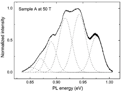
At zero field, sample A reveals a broad spectrum (122 meV overall width) with hardly any visible structure (Fig. 1). If a magnetic field of 50 T is applied parallel to the growth direction[001], the various contributions to the PL become distinguishable(Fig. 2). Since the overall width de-creases to 95 meV, the peaks are not separated by the field, meaning that the individual PL peaks become discernable because they narrow in field. Since this effect is insignificant when the field is applied in the growth plane, it shows that for sample A, the zero-field linewidth of the different contri-butions is determined mostly by variations of the wave-function extent in the growth plane; i.e., by the inhomogene-ity in the width of the wires.
The different contributions to the PL from sample B can already be seen at zero field. This shows that the size inho-mogeneity in the growth plane has improved substantially compared to that of sample A. It is therefore possible to compare the experimental peak energies with those expected from numerical calculations, using the assumption that the PL peaks originate from wires of different heights that vary by a discrete number of monolayers.2 Taking into account
that the exciton ground state is expected to consist of an electron bound to a heavy hole, the best correspondence in peak separation is found for wire heights from 6 to 13 ML (1 ML= 0.303 nm for bulk InAs)for the high- to low-energy peaks, respectively, and with the calculated peak energies shifted up by 39 meV(Fig. 3). Such a shift is justified
be-cause of the uncertainty in the band offsets.5In comparison
with data obtained on other samples and with values calcu-lated using an eigenfunction expansion method(as reported in Ref. 2), we find that the peaks originate from wires that are one monolayer thinner, which is in better correspondence with the heights obtained by AFM for those data.2
[image:4.612.59.291.54.228.2]The overall broadness of sample B complicates the analy-sis of the in-field data due to technical limitations. Therefore, qualitative results are only obtained for the peak at 0.94 eV, which is the most intense and has a relatively large separa-tion from the other peaks. From Fig. 3, the PL at 0.94 eV is FIG. 2. In a high field of 50 T, the different contributions to the
[image:4.612.320.553.54.240.2]PL of sample A become narrower and are clearly distinguishable. The dotted lines are the fitted Gaussian contributions.
FIG. 3. PL peak energies as a function of the quantum wire height in the adiabatic approximation for heavy hole excitons
(solid). The circles correspond to the peak positions for sample B and the squares to those of sample C. The triangles represent data from Ref. 2 and are shifted to the left by one monolayer. The dashed curve shows the calculated heavy-hole exciton PL peak energies shifted up by 39 meV.
assigned to annihilation of an exciton bound to a 7 ML(or 2.1 nm)high wire. When applying a magnetic field parallel to[110], the exciton wave-function extent in the direction of the wire height is investigated, and thus a parabolic field dependence of the diamagnetic shift might be expected up to 50 T due to the small wire height. However, when the PL energy is plotted against B2 (Fig. 4) a clear deviation from
the linear behavior is detected. The exciton wave-function size is thus much larger than the wire height of 2.1 nm. A magnetic length of 2.1 nm corresponds to 149 T, whereas the deviation starts at 36 T, as indicated by the arrow in Fig. 4. Such a field gives a magnetic length of 4.3 nm and a
具2典1/2 of 6.0 nm using the model from Ref. 25. The data
therefore demonstrate that the quantum wire is too thin to enclose a large portion of the wave function, which must be partially located in the InP matrix above and/or below the InAs wire. Such a penetration of the wave function into the barrier material is common in nanostructures that have weak charge localization, such as in GaAs/ AlGaAs quantum wires formed by junction of quantum wells10 or by a bend in a
well,11,12but was not anticipated in the samples under study due to the large conduction and valence band offsets of 657
and 350 meV, respectively. For comparison, the conduction band offset is 225 meV for GaAs/ Al0.3Ga0.7As quantum
wires,1279 meV for In
0.1Ga0.9As/ GaAs quantum wells,5and
120 meV for Ge/ Si quantum dots.14
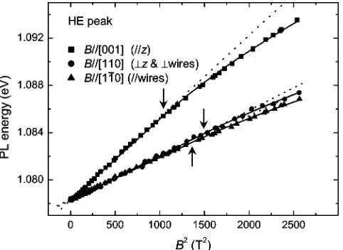
Sample C, which has a less broad overall spectrum and well-separated peaks, is best suited for analysis of the dia-magnetic energy shift. Due to the low number of peaks, it is not possible to compare the curvature in peak energy versus wire height with the numerical PL energies of Fig. 3. How-ever, because of the larger growth temperature, and thus a larger As/ P exchange during the capping procedure,4there is
less InAs present in the wire than for sample B, and reduced dimensions are expected for the wire height and/or width. By comparing the PL energies with those of sample B, wire heights of 4 and 5 ML are estimated for the high-energy (HE) and low-energy (LE) peaks, respectively (Fig. 3). In Fig. 5 the PL energy of the HE peak is plotted as a function of B2 for all three field directions. They are analyzed with
aforementioned set of expressions25and the dashed lines are
the extrapolation of the parabolic dependence. It is clear from these extrapolations that all three curves deviate from a linear B2 dependence. The crossover fields as provided by
our model are given in Table II, together with the corre-sponding exciton extents. Note that, as mentioned in Sec. III, for crossover fields this close to the maximum obtainable field, these sizes are a qualitative measure of the exciton extent rather than of the real exciton radius. For B//关110兴, the clear deviation from the linear B2behavior for the HE peak
[image:5.612.314.559.55.238.2]reflects the vertical spread of the wave function into the InP, which we also observed for sample B. Since in the 共110兲 TABLE II. PL energies, crossover fields, and associated exciton
extents for the two pronounced peaks of sample C and all three field directions.
Peak Field direction Crossover
field(T)
Exciton extent(nm)
LE共1.03 eV兲 [001]共B//z兲 37.7 5.9
关110兴 共B//wires兲 43.5 5.5
[110] 艌43.5 艋5.5
HE共1.08 eV兲 [001]共B//z兲 32.1 6.4
关110兴 共B//wires兲 36.7 6.0
[image:5.612.55.296.56.232.2][110] 38.6 5.8
FIG. 5. The same as Fig. 4, but now for the HE peak of sample C where the magnetic field is applied along the three different crys-tallographic directions indicated in the inset of Fig. 1. The arrows indicate the crossover fields. The dashed lines are extrapolations of the parabolic field dependence.
[image:5.612.53.296.617.733.2]FIG. 6. The same as Fig. 5, but now for the LE peak of sample C.
[image:5.612.314.561.634.710.2]plane(the wire cross section), the direction of strongest con-finement is[001], the diamagnetic shift with a field applied along关110兴resembles most that of the B//关110兴situation, as can be seen in Fig. 5 and Table II.
The LE peak of sample C has a less obvious sublinear dependence on B2for B//关110兴, and for B//关110兴a deviation
from the linear behavior is not even detected(Fig. 6). The latter means that the crossover field is larger than that for
B//关110兴and thus that 5.5 nm is an upper limit for the exci-ton extent in the wire height direction(Table II). If we now compare the exciton extents for B//关110兴and both peaks, we observe a decrease from 5.8 to 艋5.5 nm for increasing wire height. This means that the exciton extent significantly decreases as the wires becomes thicker and a larger portion of the exciton wave function is confined to the InAs quantum wire.
The inverse relation of the exciton extent to the wire height is clarified by Fig. 7, where a schematic diagram of a wave function confined to a nanostructure is given. If the potential well is not too narrow, a decrease in size leads to a shrinkage of the wave-function extent; i.e., in Fig. 7(b) the extent is smaller than in Fig 7(a). However, if it is made even thinner, the confinement energy becomes comparable to the band offset. This causes the wave function to signifi-cantly spread out into the barrier material and thus to in-crease its extent with decreasing wire height[compare Figs. 7(b)and 7(c)].
Calculated contour plots of the electron and heavy-hole wave functions reveal that for a wire height of 5 ML, the electron radius is much larger than that of the heavy hole in the direction of the wire height, and that the electron is in-deed substantially spread out into the InP[Fig. 8 insets(a) and (b)]. This is made more quantitative in Fig. 8 by the calculation of the percentage of the electron and hole wave function inside the quantum wire as function of the height of the quantum wire for a width of 180 Å. We now make a qualitative comparison of the numerical electron
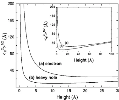
wave-function radius with the experimental exciton extent. The theoretical data confirm the inverse dependence on the wire height up to 8 ML共24.24 Å兲 for the electron (Fig. 9). Be-tween 4 and 5 ML the theoretical decrease in the electron wave-function radius with wire height is found to be 9%, which corresponds reasonably well with the experimental de-crease in exciton wave-function extent of艌5% between HE and LE of sample C. For these flat wires, a considerable portion of the electron wave function is indeed found to be located above and below the quantum wire, i.e., 61% and 51% for heights of 4 and 5 ML, respectively(Fig. 8), result-ing in respective electron wave-function radii of 2.9 and 2.6 nm in the[001]direction(Fig. 9).30The calculated elec-tron wave-function radius for the 4 ML 共12.12 Å兲 wire is thus almost five times larger than for a fully confined elec-tron, for which the radius would be approximately half the wire height.
The wire height at which the exciton wave function is smallest indicates the regime in which the wave-function spillover starts to be significant, and is found to be at 8 ML
共24.24 Å兲. This is only a factor of 2 smaller than the 50 Å that was experimentally and theoretically deduced for the In0.1Ga0.9As/ GaAs quantum well structures,9,15,17 although
the confining potential for the electron is about five times larger in the InAs/ InP wires.5
V. CONCLUSIONS
[image:6.612.334.537.54.224.2]Magnetophotoluminescence experiments and theoretical calculations within the effective-mass approximation were combined to study the charge confinement in self-assembled InAs/ InP quantum wire samples. Despite the large conduc-tion band offset, the confinement energy for thin wires is large enough to cause a considerable portion of the electron wave function to be located outside the wire in the direction of the wire height. In this regime, a decrease of the electron wave-function extent is experimentally observed for increas-ing wire height in agreement with the theoretical calcula-tions.
[image:6.612.64.283.54.228.2]FIG. 8. Probability of(a)the electrons and(b)the heavy holes to be inside the quantum wire as a function of the wire height. The insets are the contour plots of the(a)electron and(b) heavy-hole wave functions confined to a quantum wire with height 5 ML 共15.15 Å兲and width 180 Å.
The wave-function penetration into the barrier is a crucial aspect that has to be kept in mind for applications since it reduces the electron-hole overlap and augments carrier escape at room temperature. To avoid these effects, growth procedures should be focused on enhancing the size uniformity of wires(and dots)with a height of at least 8 ML.
ACKNOWLEDGMENTS
This work is supported by the Belgian Science Policy and the Flemish Science Foundation(FWO-Vl), the VIS projects of the KU Leuven and the UAntwerpen, the Nanoself project (TIC2002-04096-C03), and the NANOMAT project of the EC Growth program Contract No. G5RD-CT-2001-00545. B. P. is a post-doctoral researcher with the FWO-Vl.
*Electronic mail: [email protected]
1J. M. García, L. González, M. U. González, J. P. Silveira, Y.
González, and F. Briones, J. Cryst. Growth 227, 975(2001). 2B. Alén, J. Martínez-Pastor, A. García-Cristobal, L. González,
and J. M. García, Appl. Phys. Lett. 78, 4025(2001).
3L. González, J. M. García, R. García, F. Briones, J.
Martínez-Pastor, and C. Ballesteros, Appl. Phys. Lett. 76, 1104(2000). 4M. U. González, J. M. García, L. González, J. P. Silveira, Y.
González, J. D. Gómez, and F. Briones, Appl. Surf. Sci. 188, 188(2002).
5I. Vurgaftman, J. R. Meyer, and L. R. Ram-Mohan, J. Appl. Phys.
89, 5815(2001).
6J. Downes and D. Faux, J. Appl. Phys. 77, 2444(1995).
7C. Yi-Ping Chao and S. Chuang, Phys. Rev. B 46, 4110(1992).
8J. M. Worlock, F. M. Peeters, H. M. Cox, and P. C. Morais, Phys.
Rev. B 44, 8923(1991).
9K. Oettinger, Al. L. Efros, B. K. Meyer, C. Woelk, and H.
Brug-ger, Phys. Rev. B 52, R5531(1995).
10G. W. Bryant and Y. B. Band, Phys. Rev. B 63, 115304(2001).
11R. Rinaldi et al., Phys. Rev. Lett. 73, 2899(1994).
12G. Creci and G. Weber, Semicond. Sci. Technol. 14, 690(1999).
13H. Akiyama, J. Phys.: Condens. Matter 10, 3095(1998).
14L. Vescan, T. Stoica, and B. Holländer, Mater. Sci. Eng., B 89, 49
(2002).
15S. N. Walck and T. L. Reinecke, Phys. Rev. B 57, 9088(1998).
16A. Balandin and S. Bandyopadhyay, Phys. Rev. B 52, 8312
(1995).
17A. Thilagam, Physica B 262, 390(1999).
18H. M. Cox, D. E. Aspnes, S. J. Allen, P. Bastos, D. M. Hwang, S.
Mahajan, M. A. Shahid, and P. C. Morais, Appl. Phys. Lett. 57,
611(1990).
19K. Kash, R. Bhat, D. D. Mahoney, P. S. D. Lin, A. Scherer, J. M.
Worlock, B. P. Van der Gaag, M. Koza, and P. Grabbe, Appl. Phys. Lett. 55, 681(1989).
20A. P. Roth, P. Finnie, S. Charbonneau, C. Lacelle, C. Guérini, J.
Fraser, M. Buchanan, and Y. Feng, Microelectron. J. 28, 909
(1997).
21S. Raymond, S. Studenikin, S.-J. Cheng, M. Pioro-Ladrière, M.
Ciorga, P. J. Poole, and M. D. Robertson, Semicond. Sci. Technol. 18, 385(2003).
22R. P. Schneider Jr. and B. W. Wessels, J. Appl. Phys. 70, 405
(1991).
23F. Guffarth, R. Heitz, A. Schliwa, K. Pötschke, and D. Bimberg,
Physica E(Amsterdam) 21, 326(2004).
24J. Maes, M. Hayne, M. Henini, F. Pulizzi, A. Patanè, L. Eaves,
and V. V. Moshchalkov, Physica B 346–347, 428(2004). 25M. Hayne, R. Provoost, M. K. Zundel, Y. M. Manz, K. Eberl, and
V. V. Moshchalkov, Phys. Rev. B 62, 10324(2000).
26K. L. Janssens, F. M. Peeters, and V. A. Schweigert, Phys. Rev. B
63, 205311(2001).
27E. Alphandéry, R. J. Nicholas, N. J. Mason, S. G. Lyapin, and P.
C. Klipstein, Phys. Rev. B 65, 115322(2002).
28A. Shik, Quantum Wells: Physics and Electronics of
Two-dimensional Systems(World Scientific, Singapore, 1997). 29O. Stier, M. Grundmann, and D. Bimberg, Phys. Rev. B 59, 5688
(1999).
30Very recent calculations, which also include the effect of